

Page 1
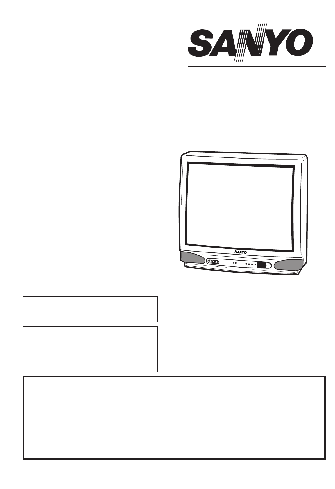
Colour Television
Service Manual
Give complete "SERVICE REF. NO." for parts
order or servicing, it is shown on the rating sheet
on the cabinet back of the TV set.
Note
This TV receiver will not work properly in foreign
countries where the television transmission
system and power source differ from the design
specifications. Refer to the specifications for the
design specifications
Contents
Safety precautions/Specifications . . . . . . . . . . . . . . . . . . . . . . . . . . . . . . . . . . . . . . . . . . . . . . . . . . . . . .2
Block diagram . . . . . . . . . . . . . . . . . . . . . . . . . . . . . . . . . . . . . . . . . . . . . . . . . . . . . . . . . . . . . . . . . . . . .3
Circuit description . . . . . . . . . . . . . . . . . . . . . . . . . . . . . . . . . . . . . . . . . . . . . . . . . . . . . . . . . . . . . . . .4-5
Cabinet Disassembly . . . . . . . . . . . . . . . . . . . . . . . . . . . . . . . . . . . . . . . . . . . . . . . . . . . . . . . . . . . . . . .6
Service control adjustment . . . . . . . . . . . . . . . . . . . . . . . . . . . . . . . . . . . . . . . . . . . . . . . . . . . . . . . . . . .7
Circuit alignment . . . . . . . . . . . . . . . . . . . . . . . . . . . . . . . . . . . . . . . . . . . . . . . . . . . . . . . . . . . . . . . . . . .8
Important notice . . . . . . . . . . . . . . . . . . . . . . . . . . . . . . . . . . . . . . . . . . . . . . . . . . . . . . . . . . . . . . . . . . .9
Special Function . . . . . . . . . . . . . . . . . . . . . . . . . . . . . . . . . . . . . . . . . . . . . . . . . . . . . . . . . . . . . . . . . .10
Cabinet Parts List . . . . . . . . . . . . . . . . . . . . . . . . . . . . . . . . . . . . . . . . . . . . . . . . . . . . . . . . . . . . . . . . .11
Electrical Parts List . . . . . . . . . . . . . . . . . . . . . . . . . . . . . . . . . . . . . . . . . . . . . . . . . . . . . . . . . . . . .12-20
Model CE28SN3-C
Service Ref.No.: CE28SN3-C-12
PRODUCT CODE: 111328207
ORIGINAL VERSION: Chassis No.: EB4-A (MKII)
Part No. SKSM0280 F2ZHY November 1999
CE28SN3-C
Page 2

-2-
EB4 MKII chassis
SAFETY PRECAUTION
X-RADIATION PRECAUTION
The primary source of X-RADIATION in the television receiver is the picture tube. The picture tube is specially
constructed to limit X-RADIATION emissions. For continued X-RADIATION protection, the replacement tube must
be the same type as the original including suffix letter. Excessive high voltage may produce potentially hazardous
X-RADIATION. To avoid such hazards, the high voltage must be maintained within specified limit. Refer to this
service manual, high voltage adjustment for specific high voltage limit. If high voltage exceeds specified limits,
take necessary corrective action. Carefully follow the instructions for +B1 volt power supply adjustment, and high
voltage adjustment to maintain the high voltage within the specified limits.
PRODUCT SAFETY NOTICE
PRODUCT SPECIFICATIONS
Product safety should be considered when a component replacement is made in any area of a receiver.
Components indicated by mark in the parts list and the schematic diagram designate components in which
safety can be of special significance. It is particularly recommended that only parts designated on the parts list in
this manual be used for component replacement designated by mark . No deviations from resistance wattage
or voltage ratings may be made for replacement items designated by mark .
!!!
1: An isolation transformer should be connected in the
power line between the receiver and the AC line
when a service is performed on the primary of the
converter transformer of the set.
2: Comply with all caution and safety-related notes
provided on the cabinet back, inside the cabinet, on
the chassis or the picture tube.
3: When replacing a chassis in the cabinet, always be
certain that all the protective devices are installed
properly, such as, control knobs, adjustment covers
or shields, barriers, isolation resistor-capacitor
networks etc.Before returning any television to the
customer, the service technician must be sure that it
is completely safe to operate without danger of
electrical shock.
Power source AC 220~240V, 50Hz
Television system System B/G
Colour system PAL/NTSC 4.43
Receiving channel VHF: E2-E12
CATV: X, Y, Z, S1-S41
UHF: #21~69
Aerial input impedance 75 ohm
AV terminal
21 Pin socket AV1: CENELEC standard (with RGB/S-inputs)
AV2: CENELEC standard
AV2: RCA Terminal, Video anf Audio (L/R) input
Sound output (Music) 12 watts x 2
Picture tube 70cm diagonal, 110 degree
(Visible picture diagonal) 66cm
Dimensions (WxHxD) 628 x 567 x 469mm
Weight 30.4 Kg
Page 3
-3-
EB4 MKII chassis
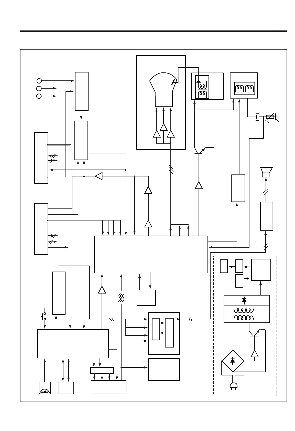
BLOCK DIAGRAM
This is a diagram for all models and therefore differs slightly from the actual block diagram.
IC801
CPU
21P Scart: AV1
21P Scart: AV2
IC201
IF/Video/Chroma/Def.
IC1202
CVBS int/ext sw.
IC1201
CVBS AV2 sw.
CRT Unit
FBT
DY
IC001
Audio Output
IC501
Vert. Output
T611
Converter Transformer
Power Supply Circuit
SIF Unit
Audio Unit
Tuner
IC802
Memory
47
49
50
SCL
SDA
RC Pre.amp
6
5
51
52
IC810
Band sw.
14
24
17
18
234
5
2: Bright 3: Contranst
4: Colour 5: Sharpness
Control Keys
10
VL
VH
U
IF
TU
1
16
45/46
28/29
30/31
41
48
37
18
19
20
7
13
15
21
22
23
24
X131
SAW Filter
IC271
1H Delay
R-Y/B-Y
R-Y/B-Y
CVBS In
Functuin In(AV1/AV2)
11/12
14/16
B
G
R
BLK
External CVBS in
Internal CVBS in
Q151 Q152/Q154
H-Drive
Q431
Q432
H-Outpit
V-Drive
V-Feedback
Audio In
Speakers
VR501
C512
H
V
HV
Q2601
Q2611
Q2621
Video In
Audio In
L R
Q171
1
6
3
8 Out
4 Out
2
7
Audio I/O
Audio I/OVideo I/O
Video I/O
RGB/BLK In
B1: 150V
B2: 25V
B3: 15V
B4: 24V
IC651
IC652
B6: 12V
B8: 5V
L, R
L, R
1/ 5
10/ 8
AC In
Q612
Q613
V-In
V-In
R
G
B
CVBS In
AV1 I/O
SIF In
Audio Out L, R
4
2
IC653
B6: 12V
B7: 8V
3D Surround
Decoder
Nicam & Stereo
Decoder
AV2 I/O
Front In
Audio
Page 4

-4-
EB4 MKII chassis
1. POWER SUPPLY
The power supply circuit of the EB4-A chassis is
composed of a rectifier smoothing circuit, an oscillation
circuit, a control circuit and an output rectifier circuit. The
AC input voltage is full-wave rectified by the rectifier
smoothing circuit, and an unstable DC voltage is
generated at both terminals of the smoothing capacitor
C607. This voltage is input to the oscillation circuit. The
oscillation circuit is provided with a blocking oscillator
circuit that switches the switching transistor Q613 ON
and OFF, and an oscillation frequency and a duty square
wave pulse are generated in the input windings
according to operation of the control circuit. A squarewave pulse whose size is dependent on the turn ratio of
the input and output windings is obtained in the output
winding. This is rectified in the output rectifier circuit, and
the desired DC voltage is obtained.
2. IF & DEFLECTION (TDA8361)
The IF output signal from the tuner passes through the
SAW filter, and it is input to pin45 and pin46 of IC201.
The signal input to the IC passes through the IF
amplifier, video detection and video amplifier circuits and
is output from pin7 as a composite video signal. And
after this signal is converted to impedance at Q151,
supplies to the video and chroma amplifier stages.
The sync.-separation circuit separates the video signals
applied to pin13(internal video signal) or pin15(external
video signal) to vertical- and horizontal-sync. signals
respectively. The horizontal oscillator requires no
external components and is fully integrated. The
oscillator is always running when the start-pin36 is
supplied with 8V. Horizontal drive signal is output from
pin37. VR361 is for adjustment of the horizontal centring.
The separated vertical-sync. signal from sync. separation
circuit passes through the vertical-separation circuit, and
applied to trigger divider circuit. The horizontal oscillation
pulse and input vertical sync. pulse are monitored by the
trigger divider circuit, and switching 50Hz and 60Hz
system, the vertical amplitude automatically adjusted for
50Hz and 60Hz. The output signal from the trigger
divider is triggered vertical oscillation circuit consisting of
C351, R352 and pin42, and vertical drive pulse is output
from pin43. VR501 is for changing the amount of AC
feedback applied to pin41 and for adjustment of the
vertical amplitude.
3. VIDEO CHROMA & R.G.B. (TDA8361)
The composite video signal output from the pin7 of
IC101 passes through Q151-Q154, and it is supplied to
pin13. The external video signal output from SCART is
supplied to pin15. The video signal input to pin13 or
pin15 is separated to luminance (Y) signal and chroma
signal in IC201. These pins are used in common with
H/V-sync. separation input. The peaking of Y signal is
adjusted by DC voltage of pin14. (“SHARPNESS”
control) The chroma signal is divided into R-Y and B-Y
chroma signals, demodulated in IC201, and output from
pin30 (R-Y) and pin31 (B-Y). These chroma signals pass
through the 1H delay line circuit (IC271), and they are
input to pin29 (R-Y) and pin28 (B-Y). These R-Y/B-Y
signals pass through RGB matrix circuit and RGB
selector circuit of IC101. The internal RGB signals are
generated in RGB matrix circuit and the RGB selector,
consisting linear amplifiers, clamps and selects either the
internal RGB signals or the external RGB signals input
from pin22(R), pin23(G), pin24(B). Selection is controlled
by the voltage at the RGB switch control (pin21) and
mixed RGB modes are possible since RGB switching is
fast. The RGB switch also functions as a fast blanking
pin by blanking the RGB output stages; here internal and
external RGB signals are overruled. The colour gain is
controlled by DC voltage of pin26. (“COLOUR” control)
The contrast control voltage present at pin25, and the
brightness control voltage present at pin17 controls DC
level of RGB signals. The RGB signals are finally
buffered before being available at the RGB output pins
[pin20 (R), pin19 (G), pin18 (R)].
4. AUDIO OUTPUT(TDA7263M)
The audio signals output from the audio unit are input to
pin1(L) and 5(R) of IC171 and passes through the preamplifier circuit and drive circuit, after which it is input to
the audio amplifier. The audio amplifier is an SEPP
(single-ended, push-pull) OTL type and output to pin8(R)
and 10(L) to directly drive the speakers.
5. VERTICAL OUTPUT (LA7832/LA7832)
An IC (LA7832/LA7833) is used for the vertical output
circuit in this chassis. The vertical drive pulse from pin43
of IC201 is input to pin4 of IC501. This pulse drives
IC501, and vertical scanning is performed. In the first half
of scanning a deflecting current is output from pin2 and
passes through the following path:
Vcc(B4) ➞ D501 ➞ pin3 ➞ pin2 ➞ DY ➞ C512 ➞
VR501/R509. An electric charge is then stored in C512.
In the last half of scanning the current path is C512 ➞
DY ➞ pin2 ➞ pin1 ➞ VR501/R509 ➞ C512. In this way,
an amplifying sawtooth waveform current flows directly to
DY to perform electron beam defection. Next, in the first
half of the banking period the vertical drive pulse
suddenly becomes OFF, and in order to reduce the
current flowing to DY, the current path becomes as
follows by the inductance of DY:
DY ➞ pin2 ➞ pin1 ➞ VR501/R509 ➞ C512 ➞ DY. Also,
when the charge of DY has dissipated, the current path
becomes Vcc24V ➞ pin6 ➞ pin7 ➞ C502 ➞ pin3 ➞
pin2➞ DY ➞ C512 ➞ VR501/R509, and when the
prescribed current value is reached, the vertical drive
pulse becomes ON. This completes one cycle.
CIRCUIT DESCRIPTION
Page 5

-5-
EB4 MKII chassis
6. HORIZONTAL OUTPUT
A horizontal oscillation signal is output from pin37 of
IC201 and switches the drive transistor Q431. This
switching signal is current amplified by the drive
transformer T431 and drives the output transistor Q432.
When Q432 becomes ON, an amplifying current flows
directly to DY through C441 ➞ DY ➞ 0432 ➞ GND, and
defection is performed in the last half of the scanning
period. Next, when Q432 becomes OFF, the charge that
had been stored in DY up to that point releases a
resonance current to the resonant capacitors C421/C423
and charges them. The current stored in C421/C423 is
then flowed back to DY, and an opposite charge is then
stored in DY. This opposite charge then switches the
dumper diode in Q432 ON, the resonance state is
completed, and an amplifying current is then flowed
again directly to DY through the dumper diode. By this
means, deflection in the first half of the scanning period
is performed, and when Q432 becomes ON at the end of
the first half of the scanning period, deflection during the
last half is begun, thus completing one cycle.
In the PCC circuit consisting of Q461 and Q462, the
parabola signal supplied from the vertical circuit is added
at the horizontal output stage and pincushion
compensation is performed by varying the DC voltage
bias. Further, the ABL voltage is feedback to the base of
Q462 to compensate for width variations due to
variations in the beam current.
7. CPU <System and Teletext Control>
Pin description
Pin1: Tuning voltage output
Pin2: Brightness control output (6-bit DAC)
Pin3: Contrast control output (6-bit DAC)
Pin4: Colour control output (6-bit DAC)
Pin5: Sharpness control output(6-bit DAC)
Pin6: Not used (GND)
Pin7: Not used (GND)
Pin8: Power ON/OFF output (H:ON)
Pin9: AFT signal input
Pin10: Option SW1 & Keyboard scan input (DC)
Pin11: Option SW2
Pin12: 50/60Hz switch input (50Hz: Hi)
Pin13: GND
Pin14: TV/AV switch output (TV: Hi)
Pin15: S-VHS switch output (S-VHS: Hi)
Pin16: Option SW3 (2AV: Hi)
Pin17: Function signal input for SCART1
Pin18: Function signal input for SCART2
Pin19: Power LED drive output1
Pin20: Option SW4 & Power LED drive output2
Pin21: Ignore output
Pin22: GND
Pin23: CVBS input0 (Internal)
Pin24: CVBS input1 (Internal/External)
Pin25: Black
Pin26: IREF
Pin27: Odd/Even output
Pin28: GND
Pin29: Pin30: V-deflection stop output
Pin31: RGB REF
Pin32: Blue output for OSD
Pin33: Green output for OSD
Pin34: Red output for OSD
Pin35: Blanking output for OSD
Pin36: H-sync. input (Horizontal pulse for OSD)
Pin37: V-sync. input (Vertical pulse for OSD)
Pin38~39: Supply (+5V)
Pin40: OSC GND
Pin41: Oscillator input for CPU
Pin42: Oscillator output for CPU
Pin43: Reset input
Pin44: Supply (+5V)
Pin45: Protect signal input (L:Power circuit defects)
Pin46: Ident. signal input
Pin47: R/C signal input
Pin48: Mute output in no picture
Pin49: I2C bus SCL (Serial clock)
Pin50: I2C bus SDA (Serial date)
Pin51: Option SW5 & Band select output1
Pin52: Band select output2
Page 6
-6-
EB4 MKII chassis
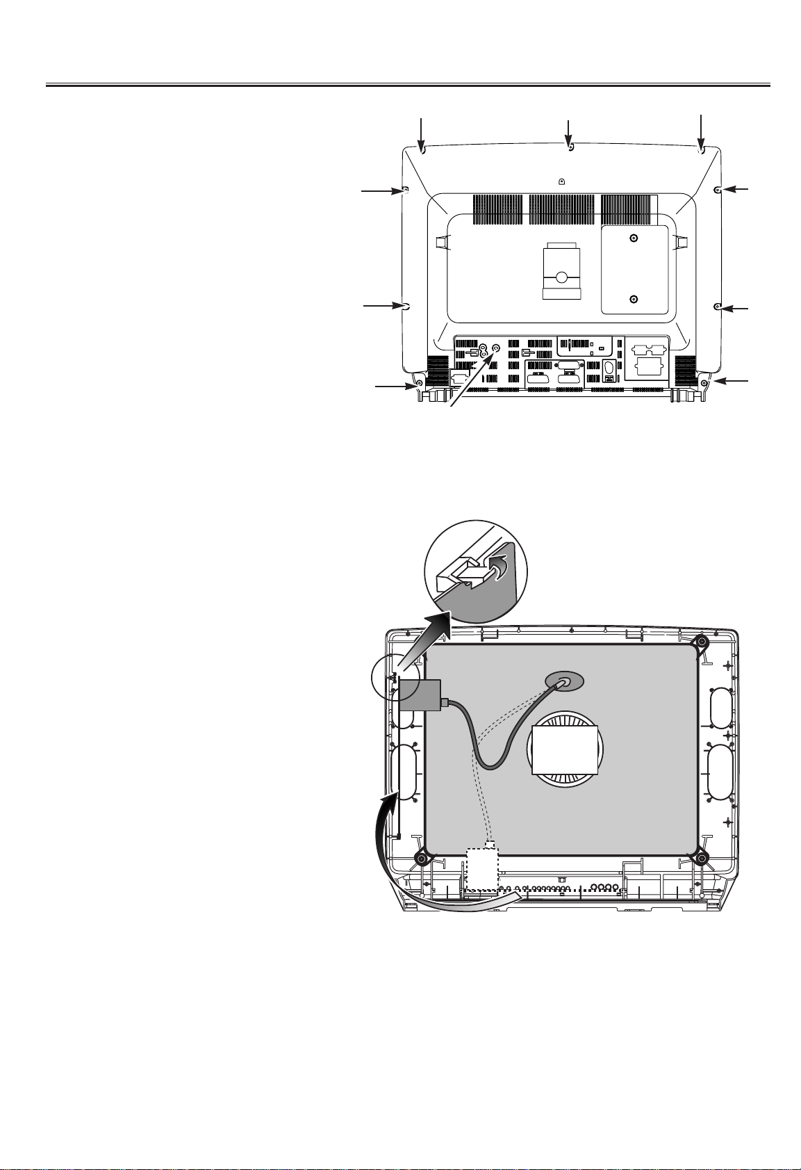
CABINET DISASSEMBLY
CABINET BACK DISASSEMBLY
1. Remove 10 screws(A).
2. Pull out the cabinet back.
PLACING THE CHASSIS TO SERVICE
POSITION
1. Pullout the chassis and put it to the rails on the
side cabinet.
2. Fix main board with hook on the top rail.
(A)
(A)
(A)
(A)
(A)
(A)
(A)
(A)
(A)
(A)
Page 7

B1 POWER SUPPLY ADJUSTMENT
1. Set VR641 to be mechanical centre before pressing
the main switch.
2. Tune the receiver to PAL circular pattern.
3. Set brightness and contrast controls to normal.
4. Connect digital V-meter to test point "TP-B".
5. By using VR641, adjust voltage to 150 ± 0.5 V.
AFT ADJUSTMENT
1. Tune the receiver to the clearest station.
2. By using T141, adjust AFT to obtain the best picture.
AGC ADJUSTMENT
NOTE:
Do not attempt this adjustment with weak
signal.
1. Tune the receiver to the clearest station.
2. Set AGC VR(VR131) in direction which causes snow
noise to appear, then in the opposite direction until
snow noise just disappears.
GREY SCALE ADJUSTMENT
[SCREEN VR ADJUSTMENT]
1. Tune the receiver to the white pattern.
2. Set brightness and contrast controls to normal.
3. Set VR602and VR612 to be mechanical centre.
4. Turn VR601, VR611 and VR621 fully counter-
clockwise.
5. Set mode to one horizontal scanning line, how to set
refer to "service mode"
6. Set screen VR for one colour to be just visible.
[BIAS VR ADJUSTMENT]
7. By using VR601, VR611 or VR621, adjust line to be
white.
8. Set screen mode OFF, how to set refer to "service
mode"
[DRIVE VR ADJUSTMENT]
9. By using VR602 and VR612, adjust white balance.
HIGH VOLTAGE & WIDTH ADJUSTMENT
[HIGH VOLTAGE ADJUSTMENT]
1. Tune the receiver to circular pattern.
2. Set brightness and contrast controls to maximum.
3. Connect digital V-meter to both terminals of R224, and
high voltage meter to CRT anode.
4. Confirm high voltage to be 26.0 ± 1 KV at beam
current 1.4, and less than 29.0 KV at 0 beam current.
[H-WIDTH ADJUSTMENT]
5. Adjust VR462 to obtain
proper H- width.
6. Reconfirm high voltage.
H-CENTRE ADJUSTMENT
1. Tune the receiver to circular
pattern.
2. Adjust H-centre by using
VR361.
V-CENTRE ADJUSTMENT
1. Tune the receiver to circular pattern.
2. Adjust V-centre by using SW501.
V-SIZE ADJUSTMENT
1. Tune the receiver to circular pattern.
2. Adjust V-size by using VR501.
FOCUS ADJUSTMENT
By using FOCUS VR, adjust focus control for good
scanning lines.
SERVICE CONTROL ADJUSTMENT
-7-
EB4 MKII chassis
SW601
Main switch
F601
Fuse
T481
RC Transformer
SW1901
Prog.+
SW1902
Prog.-
SW1903
Vol.+
SW1904
Vol.-
Q641
VR641
+B ADJ.
Q681
IC801
CPU
Q501
Q432
H-Output
IC501
V-Outout
IC651
+12V
Scart 2
SW501
V-Centre
VR501
V-Size
IC271
1H Delay
IC652
+8V
Scart 1
IC201
IF/Video/Croma/Def.
IC281
VR361
H-Centre
VR131
AGC
T101
T141
SIF Board
A101 Tuner
IC1202
Int./Ext. SW.
IC1201
AV2 SW.
TP-E
TP-
Q-SOUND Board
T611
Converter Trans
TP-B
VR462
H-Width
Q461
Q462
T451
Flyback
Transformer
R224
J213
Q501
Q432
H-Output
IC501
V-Outout
Scart 2
SW501
V-Centre
VR501
V-Size
IC271
1H Delay
Scart 1
IC201
IF/Video/Croma/Def.
IC281
VR361
H-Centre
VR131
AGC
T101
SIF Boa
A101 Tuner
IC1202
Int./Ext. SW.
IC1201
AV2 SW.
TP-E
Q-SOUND Board
T141
VR641
VR642
VR361VR501SW501
VR131
Page 8

-8-
EB4 MKII chassis
DC 15.5V
AGC voltage (4.3-4.5V)
Output probe
Input probe
Marker frequency
Sweep ATT
0dB=176mVrms/75
SETTING
C644 +
IC201-pin48
IC201-pin45
(Side b)
IC201-pin7
38.9MHz
20dB
Adjustment
By using T141, adjust "P" to
be maximum amplitude.
Waveform
CIRCUIT ALIGNMENT
VIF alignment
P
P
0.002µF
75Ω
1kΩ
a
b
10kΩ
Input probe
Output probe
SIF alignment
SIF BOARD
DC 12V
AGC voltage(5V DC)
Output probe
Input probe
Sweep ATT
Marker Frequency
Tool-A
SETTING
IC3801-pin9
IC3801-pin13
IC3801-pin5
(Side b)
IC3801-pin17
10dB
38.9MHz
IC3801-pin6
and ground
Adjustment
1. By using T3801, adjust the
VCO oscillation to be "P".
Waveform
0.01
Tool-A
IC3811
IC3801
K38H2
K38H1
T3801
Page 9

-9-
EB4 MKII chassis
When you replace a memory IC (IC802), it is
necessary to initialise the IC as following step.
A. Initialization
Press and hold the ( ) normalization button on the
remote control handset and press the ( ) programme
+ button on the TV set.
The IC will be initialised automatically to set the
following data.
User control data
Colour : Centre
Brightness : Centre
Contrast : Maximum
Sharpness : Centre
Text. Bright : Centre
Bass : Centre
Treble : Centre
Balance : Centre
Volume : Step 12
B. Service Mode
1. To enter the service mode, press and hold the ( )
Function button on the remote control handset and
press the ( )programme + button on the TV set.
The following OSD appears on the screen.
2. Select desired service item by using the ( )
Function button on the remote control handset.
3. Change date by using the ( )Level + or ()button.
4. To return to TV mode press the ( )Recall button
on the remote control handset.
Service mode description
SCREEN: For screen adjustment
To make one horizontal scanning line.
ADJUST DATA
System +000
SCREEN VOL
CPU MK2 1.0
INITIALIZATION (Important Notice)
Page 10

-10-
EB4 MKII chassis
This TV set allows you to set up the following special functions.
■ Maximum volume setting and prohibition of presetting
ITEM-1
Sets the current volume as the maximum volume level and prohibition of
presetting.
SET➞ 0 NO
SET➞ 1 YES
■ Start up programme position
ITEM-2
Presets the programme position when the set is switched on.
SET -> 0 Last programme position start
SET -> 1 Programme position "1" start
SET -> 2 Programme position "2" start
SET -> 3 Programme position "3" start
SET -> 4 Programme position "4" start
SET -> 5 Programme position "5" start
SET -> 6 Programme position "6" start
SET -> 7 Programme position "7" start
SET -> 8 Programme position "8" start
SET -> 9 "AV1" start
SETTING PROCEDURE
1
Press and hold the button on the Remote control handset
and then press the P▲ button on the TV set.
2
To select the "Item" number, press the button on the remote
control handset.
3
To select the "Set" number,press the or button
repeatedly.
4
To return to the normal TV mode, press the button.
✐The setting conditions of all items can be confirmed.
✐Special functions are not cancelled if the TV set is switched off or the
mains disconnected.
ITEM-1 SET -> 0
SPECIAL FUNCTION
Page 11

F2ZHY
-11-
CABINET PARTS LIST
CABINET PARTS
1 1KB0CAM0458-D ASSY,CABINET FR-F2ZH
2 SKTBUM0058AE UNSP BTN UNIT-F2ZE-A
3 610 262 2089 CABINET BACK-B-E6ZV
4 610 262 6742 DEC BOARD-F2ZV
5 SKTGRF1271-D ASSY GRILLE SP-R
6 SKTGRF1272-D ASSY GRILLE SP-L
7 645 003 9256 BADGE,SANYO*46.2X13.5L45
ACCESSORIES
8 JXMCA RC TRANSMITTER
SKP10160 INST MANUAL - F2Z
SKP10161 INST MANUAL - F2Z
645 000 6708 BATTERY,MANGAN,COMPOSITE
Note: Parts order must contain Service Ref. No., Part No., and descriptions.
1
2
3
4
5
6
7
89
0
-/--
P▲
▼
P
P
F
P
MENU
i
SURROUND
BASS
TV
TXT
?
X
AB
TV
4
8
1
2 65
9
3
Ref. No. Part No. Description Ref. No. Part No. Description
SERVICE REF. NO. CE28SN3-C-12
Page 12

F2ZHY
-12-
Service Ref No.: CE28SN3-C-12
Chassis construction
OUT OF CIRCUIT (Page 12)
ASSY,PWB,CRT-MK2 1AA0B10H03500 (Page 12)
ASSY,PWB,SIF 1AA0B10H0300A (Page 13)
ASSY,PWB,AUDIO 1AA0B10H0300B (Page 13)
ASSY,PWB,MAIN F2ZHY 1AA0B10H028A0 (Page 14)
OUT OF CIRCUIT BOARD
PICTURE TUBE
Q901 414 009 7203 CRT A66EHJ43X38
COIL
L901 645 025 6523 28DEG.COIL OREGA 47320235
MISCELLANEOUS
SP901 610 232 3986 SPEAKER
SP902 610 232 3986 SPEAKER
W901 645 012 7632 EURO PLUG +2P HOUSE @ 2.1
W902 610 204 6090 GROUNDING CONNECTOR-D8ZL
ASSY,PWB,CRT-MK2 1AA0B10H03500
TRANSISTOR
Q701 405 041 6507 TR 2SC2621-D-RA
405 041 6705 TR 2SC2621-E-RA
405 066 9903 TR 2SC2688(1)-K
405 067 0008 TR 2SC2688(1)-L
405 067 0107 TR 2SC2688(1)-M
Q711 405 041 6507 TR 2SC2621-D-RA
405 041 6705 TR 2SC2621-E-RA
405 066 9903 TR 2SC2688(1)-K
405 067 0008 TR 2SC2688(1)-L
405 067 0107 TR 2SC2688(1)-M
Q721 405 041 6507 TR 2SC2621-D-RA
405 041 6705 TR 2SC2621-E-RA
405 066 9903 TR 2SC2688(1)-K
405 067 0008 TR 2SC2688(1)-L
405 067 0107 TR 2SC2688(1)-M
Q740 406 007 1901 TR JC556A
406 007 1802 TR JC556B
405 004 4205 TR 2SA608-E-CTV-NP
405 004 4809 TR 2SA608-F-CTV-NP
405 028 7909 TR 2SA608-G-CTV-NP
Q751 406 007 1901 TR JC556A
406 007 1802 TR JC556B
!!!
Ref. No. Part No. Description
CHASSIS ELECTRICAL PARTS LIST
Note: Parts order must contain Service Ref. No., Part No., and descriptions.
Product safety should be considered when a component replacement is made in any area of a receiver.
Components indicated by a mark in this parts list and the circuit diagram show components whose value have
special significance to product safety. It is particularly recommended that only parts specified on the following parts
list be used for components replacement pointed out by the mark .
!
!
Read description in the Capacitor and Resistor as follows:
CAPACITOR
CERAMIC 100P K 50V
Rated Voltage
Tolerance Symbols:
Less than 10PF
A: Not specified B: ±0.1PF C: ±0.25PF
D: ±0.5PF F: ±1PF G: ±2PF
R: ±0.25-0PF S: ±0-0.25PF E: +0-1PF
More than 10PF
A: Not specified B: ±0.1% C: ±0.25%
D: ±0.5% F: ±1% G: ±2%
H: ±3% J: ±5% K: ±10%
L: ±15% M: ±20% N: ±30%
P: +100-0% Q: +30-10% T: +50-10%
U: +75-10% V: +20-10% W: +100-10%
X: +40-20% Y: +150-10% Z: +80-20%
Rated value: P=pico farad, U=Micro farad
Material:
CERAMIC.......... Ceramic
MT-PAPER........ Metallized Paper
POLYESTER..... Polyester
MT-POLYEST.... Metallized Polyester
POLYPRO.......... Polypropylene
MT-POLYPRO.... Metallized Polypropylene
COMPO FILM..... Composite film
MT-COMPO........ Metallized Composite
STYRENE........... Styrene
TA-SOLID........... Tantalum Solid
AL-SOLID........... Aluminium Solid
ELECT................ Electrolytic
NP-ELECT.......... Non-polarised Electrolytic
OS-SOLID.......... Aluminium Solid with Organic Semiconductive Electrolytic
DL-ELECT.......... Double Layered Electrolytic
RESISTOR
CARBON 4.7K J A 1/4W
Rated Wattage
Performance Symbols:
A: General B: Non flammable Z: Low noise
Other: Temperature coefficient
Tolerance Symbols:
A: ±0.05% B: ±0.1% C: ±0.25% D:±0.5%
F: ±1% G: ±2% J: ±5% K:±10%
M: ±20% P: +5-15%
Rated value, ohms:
K: 1,000, M: 1,000,000
Material:
CARBON........... Carbon
MT-FILM............ Metal Film
OXIDE-MT......... Oxide Metal Film
SOLID................ Composition
MT-GLAZE......... Metal Glaze
WIRE WOUND... Wire Wound
CERAMIC RES.. Ceramic
FUSIBLE RES.... Fusible
Page 13

405 004 4205 TR 2SA608-E-CTV-NP
405 004 4809 TR 2SA608-F-CTV-NP
405 028 7909 TR 2SA608-G-CTV-NP
CAPACITOR
C701 403 074 5712 CERAMIC 560P K 50V
C711 403 074 5712 CERAMIC 560P K 50V
C721 403 074 5712 CERAMIC 560P K 50V
C731 403 077 2728 CERAMIC 1000P P 2K
C735 403 055 8401 ELECT 22U M 250V
403 260 0405 ELECT 22U M 250V
C751 403 248 1608 ELECT 47U M 16V
RESISTOR
R701 401 026 3925 CARBON 330 JA 1/6W
R702 401 026 7022 CARBON 3K9 JA 1/6W
R703 401 024 7024 CARBON 1K JA 1/6W
R704 401 065 4604 OXIDE-MT 12K JA 2W
R705 401 009 6622 CARBON 3.3K JA 1/2W
R711 401 026 3925 CARBON 330 JA 1/6W
R712 401 026 7022 CARBON 3K9 JA 1/6W
R713 401 025 7825 CARBON 2K2 JA 1/6W
R714 401 065 4604 OXIDE-MT 12K JA 2W
R715 401 009 6622 CARBON 3.3K JA 1/2W
R721 401 026 3925 CARBON 330 JA 1/6W
R722 401 026 7022 CARBON 3K9 JA 1/6W
R723 401 025 4220 CARBON 1K8 JA 1/6W
R724 401 065 4604 OXIDE-MT 12K JA 2W
R725 401 009 6622 CARBON 3.3K JA 1/2W
R727 401 026 9620 CARBON 470 JA 1/6W
R741 401 026 9927 CARBON 4K7 JA 1/6W
R742 401 026 4328 CARBON 3K3 JA 1/6W
R744 401 026 0627 CARBON 270 JA 1/6W
R752 401 024 7430 CARBON 10K JA 1/6W
R753 401 024 7430 CARBON 10K JA 1/6W
VARIABLE RESISTOR
VR701 645 003 5722 VR,SEMI,4.7K N
VR702 645 003 5647 VR,SEMI,1K N
VR711 645 003 5722 VR,SEMI,4.7K N
VR712 645 003 5647 VR,SEMI,1K N
VR721 645 003 5722 VR,SEMI,4.7K N
COIL
L701 645 008 0012 INDUCTOR,330U K
L711 645 008 0012 INDUCTOR,330U K
L721 645 008 0012 INDUCTOR,330U K
DIODE
D701 407 012 4416 DIODE 1SS133-T-77
D711 407 012 4416 DIODE 1SS133-T-77
D721 407 012 4416 DIODE 1SS133-T-77
D751 407 012 4416 DIODE 1SS133-T-77
MISCELLANEOUS
K7M 645 008 4058 TERMINAL PLUG
K7P 645 008 7288 HOUSING PLUG 5P
K7Q 645 008 7264 HOUSING PLUG 3P
K701 645 031 7699 CRT SKT. HPS-014103
ASSY,PWB,SIF 1AA0B10H0300A
TRANSISTOR
Q3811 405 014 4519 TR 2SC2412KT146/R
INTEGRATED CIRCUIT
IC3801 409 310 8407 IC LA7577N
CAPACITOR
C3805 403 023 4414 CERAMIC 330P J 50V
C3806 403 069 9510 CERAMIC CHIP 0.01 Z 50V
C3807 403 069 9510 CERAMIC CHIP 0.01 Z 50V
C3808 403 049 4204 ELECT 10U M 50V
C3809 403 069 9510 CERAMIC CHIP 0.01 Z 50V
C3810 403 051 0607 ELECT 4.7U M 50V
C3811 403 018 0503 CERAMIC 22P J 50V
C3812 403 048 6308 ELECT 0.47U M 50V
C3813 403 074 6610 CERAMIC 560P K 50V
C3814 403 069 1712 CERAMIC 1000P K 50V
C3815 403 069 9510 CERAMIC CHIP 0.01 Z 50V
RESISTOR
R3811 401 038 7512 MT-GLAZE 56 JA 1/10W
R3812 401 037 5618 MT-GLAZE 10K JA 1/10W
R3815 401 037 5410 MT-GLAZE 1K JA 1/10W
R3816 401 038 3514 MT-GLAZE 330 JA 1/10W
R3817 401 039 0314 MT-GLAZE 820 JA 1/10W
R3818 401 037 6714 MT-GLAZE 1.2K JA 1/10W
TRANSFORMER
T3801 610 037 4539 S COIL
MISCELLANEOUS
K38H1 645 027 0185 PLUG,4P
K38H2 645 027 0185 PLUG,4P
X3801 421 007 2109 SAW F TSB5392T
ASSY,PWB,AUDIO 1AA0B10H0300B
TRANSISTOR
Q1252 405 014 4519 TR 2SC2412KT146/R
Q1253 405 014 4519 TR 2SC2412KT146/R
Q3452 405 014 4519 TR 2SC2412KT146/R
Q3453 405 014 4519 TR 2SC2412KT146/R
INTEGRATED CIRCUIT
IC1251 409 336 0508 IC BU4052BC
IC3451 409 445 1403 IC TDA9875A/V2
CAPACITOR
C1251 403 043 9106 ELECT 47U M 16V
C3452 403 314 5915 SMD CAP GRM40X5R474K16
C3453 403 026 2813 CERAMIC 47P J 50V
C3454 403 068 0419 CERAMIC 0.1U Z 25V
C3455 401 037 5014 MT-GLAZE 0.000 ZA 1/10W
C3458 403 026 2813 CERAMIC 47P J 50V
C3461 403 049 0008 ELECT 1U M 50V
C3462 401 037 5014 MT-GLAZE 0.000 ZA 1/10W
C3468 403 049 0008 ELECT 1U M 50V
C3469 403 049 0008 ELECT 1U M 50V
C3473 403 279 4312 CERAMIC 0.33U K 16V
C3474 403 279 4312 CERAMIC 0.33U K 16V
C3476 403 314 5915 SMD CAP GRM40X5R474K16
!
Ref. No. Part No. Description Ref. No. Part No. Description
-13-
F2ZHY
Page 14

C3477 403 039 2104 ELECT 47U M 6.3V
C3480 403 039 2104 ELECT 47U M 6.3V
C3481 403 039 2104 ELECT 47U M 6.3V
C3482 403 069 9510 CERAMIC CHIP 0.01 Z 50V
C3483 403 069 9510 CERAMIC CHIP 0.01 Z 50V
C3484 403 039 2104 ELECT 47U M 6.3V
C3485 403 069 9510 CERAMIC CHIP 0.01 Z 50V
C3486 403 049 0008 ELECT 1U M 50V
C3487 403 049 0008 ELECT 1U M 50V
C3490 403 009 5718 CERAMIC 100P J 50V
C3492 403 069 5611 CERAMIC 0.01U K 50V
C3493 403 069 5611 CERAMIC 0.01U K 50V
C3521 403 279 4312 CERAMIC 0.33U K 16V
C3522 403 279 4312 CERAMIC 0.33U K 16V
RESISTOR
R1251 401 038 9318 MT-GLAZE 68K JA 1/10W
R1252 401 038 9318 MT-GLAZE 68K JA 1/10W
R1253 401 038 9318 MT-GLAZE 68K JA 1/10W
R1254 401 038 9318 MT-GLAZE 68K JA 1/10W
R1255 401 038 9318 MT-GLAZE 68K JA 1/10W
R1256 401 038 9318 MT-GLAZE 68K JA 1/10W
R1257 401 038 9318 MT-GLAZE 68K JA 1/10W
R1258 401 038 9318 MT-GLAZE 68K JA 1/10W
R1261 401 038 6317 MT-GLAZE 470 JA 1/10W
R1262 401 038 0711 MT-GLAZE 2.2K JA 1/10W
R1263 401 038 6317 MT-GLAZE 470 JA 1/10W
R1264 401 038 0711 MT-GLAZE 2.2K JA 1/10W
R3451 401 037 5212 MT-GLAZE 100 JA 1/10W
R3452 401 037 5212 MT-GLAZE 100 JA 1/10W
R3453 401 037 5618 MT-GLAZE 10K JA 1/10W
R3454 401 037 5212 MT-GLAZE 100 JA 1/10W
R3455 401 037 5618 MT-GLAZE 10K JA 1/10W
R3456 401 037 5014 MT-GLAZE 0.000 ZA 1/10W
R3459 401 037 5014 MT-GLAZE 0.000 ZA 1/10W
R3462 401 037 5014 MT-GLAZE 0.000 ZA 1/10W
R3464 401 037 5212 MT-GLAZE 100 JA 1/10W
R3465 401 037 5618 MT-GLAZE 10K JA 1/10W
R3466 401 037 5410 MT-GLAZE 1K JA 1/10W
R3467 401 038 2111 MT-GLAZE 2.7K JA 1/10W
R3468 401 037 5410 MT-GLAZE 1K JA 1/10W
R3469 401 038 2111 MT-GLAZE 2.7K JA 1/10W
R3471 401 038 2012 MT-GLAZE 270 JA 1/10W
R3472 401 037 5014 MT-GLAZE 0.000 ZA 1/10W
R3473 401 038 6317 MT-GLAZE 470 JA 1/10W
R3474 401 038 0711 MT-GLAZE 2.2K JA 1/10W
R3475 401 038 6317 MT-GLAZE 470 JA 1/10W
R3476 401 038 0711 MT-GLAZE 2.2K JA 1/10W
R3477 401 038 5310 MT-GLAZE 39K JA 1/10W
R3478 401 038 5310 MT-GLAZE 39K JA 1/10W
R3479 401 037 8015 MT-GLAZE 15K JA 1/10W
R3480 401 037 8015 MT-GLAZE 15K JA 1/10W
R3515 401 037 5014 MT-GLAZE 0.000 ZA 1/10W
R3517 401 037 5014 MT-GLAZE 0.000 ZA 1/10W
R3518 401 038 0711 MT-GLAZE 2.2K JA 1/10W
COIL
L3450 401 037 5014 MT-GLAZE 0.000 ZA 1/10W
L3452 645 008 2221 INDUCTOR,2.2U K
L3456 645 008 2221 INDUCTOR,2.2U K
L3457 645 008 2221 INDUCTOR,2.2U K
L3459 401 037 5014 MT-GLAZE 0.000 ZA 1/10W
MISCELLANEOUS
J1251 401 037 5014 MT-GLAZE 0.000 ZA 1/10W
J3459 401 037 5014 MT-GLAZE 0.000 ZA 1/10W
J3463 401 037 5014 MT-GLAZE 0.000 ZA 1/10W
J3465 401 037 5014 MT-GLAZE 0.000 ZA 1/10W
J3469 401 037 5014 MT-GLAZE 0.000 ZA 1/10W
J3474 401 037 5014 MT-GLAZE 0.000 ZA 1/10W
J3486 401 037 5014 MT-GLAZE 0.000 ZA 1/10W
J3489 401 037 5014 MT-GLAZE 0.000 ZA 1/10W
K12B 645 008 7288 HOUSING PLUG 5P
K34A 645 027 0192 PLUG,10P
K34B 645 027 0192 PLUG,10P
K34C 645 027 0178 PLUG,3P
X3451 645 024 7484 OSC,CRYSTAL 24.576MHZ
ASSY,PWB,MAIN F2ZHY 1AA0B10H028A0
TRANSISTOR
Q001 406 007 2106 TR JC546A
Q1001 406 007 1901 TR JC556A
Q1002 406 007 2106 TR JC546A
Q1003 406 007 2106 TR JC546A
Q1004 406 007 2106 TR JC546A
Q1005 406 007 2106 TR JC546A
Q1041 406 007 2106 TR JC546A
Q1042 406 007 1901 TR JC556A
Q1043 406 007 2106 TR JC546A
Q1201 406 007 2106 TR JC546A
Q1202 406 007 2106 TR JC546A
Q1203 406 007 2106 TR JC546A
Q121 406 007 2106 TR JC546A
Q151 406 007 1901 TR JC556A
Q152 406 007 2106 TR JC546A
Q153 406 007 1901 TR JC556A
Q154 406 007 1901 TR JC556A
Q171 406 007 2106 TR JC546A
Q2001 406 007 2106 TR JC546A
Q201 406 007 2106 TR JC546A
Q202 406 007 2106 TR JC546A
Q431 405 018 0616 TR 2SC3332-S
Q432 406 015 2501 ON5111 (BU2708DX) PH.
Q461 405 064 7307 TR 2SB1274-Q-RA
Q461-1 610 251 5916 HEAT SINK PCC E7LC
Q461-2 411 045 2209 SCR PAN+SW 3X10
Q461-3 411 004 4404 NUT HEX 3
Q461-4 610 014 5818 WASHER
Q461-5 610 077 7613 SILICONE GREASE G-746
Q462 406 007 2106 TR JC546A
Q501 406 007 2106 TR JC546A
Q611 406 007 1901 TR JC556A
Q612 405 058 0208 TR 2SC3807-R-CTV-YA
Q613 405 095 0407 TR 2SC4429-L-YB
Q613-1 610 251 5893 POW HEAT SINK E7LC
Q613-2 411 046 8507 SCR PAN+SW+W 3X10
Q613-3 411 004 4404 NUT HEX 3
Q613-4 610 077 7613 SILICONE GREASE G-746
Q641 406 007 2106 TR JC546A
Q681 405 059 9804 TR 2SD1913-Q-RA
Q682 406 007 1901 TR JC556A
Q801 405 118 4217 TR PH2369
Q835 406 007 2106 TR JC546A
Q861 406 007 1901 TR JC556A
Q871 406 007 2106 TR JC546A
Ref. No. Part No. Description Ref. No. Part No. Description
-14-
F2ZHY
Page 15

Q872 406 007 2106 TR JC546A
Q873 406 007 2106 TR JC546A
Q874 406 007 2106 TR JC546A
INTEGRATED CIRCUIT
IC001 409 301 4906 IC TDA7263M
IC001-1 610 251 4186 AUDIO HEATSINK ASSY E7PC
IC1201 409 018 7603 IC LA7016
IC1202 409 120 3401 IC LA7221
IC201 409 380 8703 IC TDA8361/N5
IC271 409 404 0201 IC U3665M
IC501 409 192 5709 IC LA7833
IC501-1 610 251 5909 V HEAT SINK E7LC
IC651 409 365 2900 IC BA178M12T
IC652 409 365 2801 IC BA178M08T
IC653 409 241 5407 IC BA178M05T
IC654 409 367 2809 IC BA178M09T
IC801 410 317 2909 IC SAA5296ZP/092
IC802 409 333 3700 IC 24LC02B/P
IC810 409 019 6209 IC LA7910
CAPACITOR
C001A 403 068 0419 CERAMIC 0.1U Z 25V
C002 403 070 9813 CHIP CERAMIC 0.015U K 50V
C003A 403 068 0419 CERAMIC 0.1U Z 25V
C004 403 070 9813 CHIP CERAMIC 0.015U K 50V
C005 403 046 3507 ELECT 33U M 25V
C006 403 046 3507 ELECT 33U M 25V
C007 403 237 7941 MT-COMPO 0.22U J 50V
C008 403 237 7941 MT-COMPO 0.22U J 50V
C009 403 237 7941 MT-COMPO 0.22U J 50V
C010 403 237 7941 MT-COMPO 0.22U J 50V
C011 403 045 1504 ELECT 1000U M 25V
C012 403 045 1504 ELECT 1000U M 25V
C013 403 069 9510 CERAMIC CHIP 0.01 Z 50V
C014 403 069 9510 CERAMIC CHIP 0.01 Z 50V
C015 403 044 9501 ELECT 100U M 25V
C016 403 085 4008 NP-ELECT 10U M 16V
C017 403 085 4008 NP-ELECT 10U M 16V
C020 403 069 0507 CERAMIC 1000P K 50V
C021 403 052 8503 ELECT 1000U M 35V
C023 403 069 9510 CERAMIC CHIP 0.01 Z 50V
C024 403 069 9510 CERAMIC CHIP 0.01 Z 50V
C100 403 248 1618 ELECT 47U M 16V
C1001 403 069 1712 CERAMIC 1000P K 50V
C1002 403 049 4204 ELECT 10U M 50V
C1003 403 009 5718 CERAMIC 100P J 50V
C1004 403 130 3119 CERAMIC 0.047U K 50V
C1005 403 069 1712 CERAMIC 1000P K 50V
C1006 403 049 4204 ELECT 10U M 50V
C1007 403 009 5718 CERAMIC 100P J 50V
C1008 403 130 3119 CERAMIC 0.047U K 50V
C1009 403 049 4204 ELECT 10U M 50V
C101 403 194 4609 ELECT 470U M 16V
C102 403 043 9106 ELECT 47U M 16V
C103A 403 069 1712 CERAMIC 1000P K 50V
C1021 403 069 1712 CERAMIC 1000P K 50V
C1022 403 049 4204 ELECT 10U M 50V
C1023 403 009 5718 CERAMIC 100P J 50V
C1024 403 041 9405 ELECT 10U M 16V
C1025 403 069 1712 CERAMIC 1000P K 50V
C1026 403 049 4204 ELECT 10U M 50V
C1027 403 009 5718 CERAMIC 100P J 50V
C1028 403 041 9405 ELECT 10U M 16V
C1029 403 049 4204 ELECT 10U M 50V
C1031 403 033 4510 CERAMIC 82P J 50V
C104B 403 043 9106 ELECT 47U M 16V
C1041 403 049 4204 ELECT 10U M 50V
C106 403 049 0008 ELECT 1U M 50V
C106A 403 069 9510 CERAMIC CHIP 0.01 Z 50V
C107A 403 069 1712 CERAMIC 1000P K 50V
C107B 403 069 9510 CERAMIC CHIP 0.01 Z 50V
C108 403 027 1211 CERAMIC 5P J 50V
C109 403 027 1211 CERAMIC 5P J 50V
C110 403 033 4510 CERAMIC 82P J 50V
C1101 403 049 4204 ELECT 10U M 50V
C1103 403 069 1712 CERAMIC 1000P K 50V
C1104 403 049 4204 ELECT 10U M 50V
C1106 403 069 1712 CERAMIC 1000P K 50V
C1107 403 049 4204 ELECT 10U M 50V
C1108 403 033 4510 CERAMIC 82P J 50V
C1109 403 008 7416 CERAMIC 10P D 50V
C114 401 037 5014 MT-GLAZE 0.000 ZA 1/10W
C117 401 037 5014 MT-GLAZE 0.000 ZA 1/10W
C1200 403 069 9510 CERAMIC CHIP 0.01 Z 50V
C1201 403 049 4204 ELECT 10U M 50V
C1202 403 049 4204 ELECT 10U M 50V
C1203 403 069 8305 CERAMIC 0.01U Z 50V
C121 403 068 0419 CERAMIC 0.1U Z 25V
C131 401 037 5014 MT-GLAZE 0.000 ZA 1/10W
C132 403 069 1712 CERAMIC 1000P K 50V
C133 403 069 9510 CERAMIC CHIP 0.01 Z 50V
C134 403 049 9803 ELECT 2.2U M 50V
C135 403 068 0419 CERAMIC 0.1U Z 25V
C136 403 194 4609 ELECT 470U M 16V
C137 403 068 0419 CERAMIC 0.1U Z 25V
C138 403 069 9510 CERAMIC CHIP 0.01 Z 50V
C141 403 028 4419 CERAMIC 56P J 50V
C142 403 068 0419 CERAMIC 0.1U Z 25V
C143 403 027 1211 CERAMIC 5P J 50V
C146 403 010 8507 CERAMIC 12P J 50V
C151 403 024 2112 CERAMIC 39P J 50V
C162 403 068 2512 CERAMIC 0.22U Z 25V
C171 403 237 8057 MT-COMPO 0.1U J 50V
C1901 403 069 1712 CERAMIC 1000P K 50V
C200 403 068 0419 CERAMIC 0.1U Z 25V
C2001 403 068 0419 CERAMIC 0.1U Z 25V
C2002 403 068 0419 CERAMIC 0.1U Z 25V
C2003 403 068 0419 CERAMIC 0.1U Z 25V
C201 403 014 3409 CERAMIC 18P J 50V
C202 403 237 8057 MT-COMPO 0.1U J 50V
C203 403 073 9117 CERAMIC 4700P K 50V
C204 403 068 0419 CERAMIC 0.1U Z 25V
C205 403 068 0419 CERAMIC 0.1U Z 25V
C206 403 068 0419 CERAMIC 0.1U Z 25V
C207 403 068 0419 CERAMIC 0.1U Z 25V
C208 403 068 0419 CERAMIC 0.1U Z 25V
C209 403 069 1712 CERAMIC 1000P K 50V
C212 403 049 9803 ELECT 2.2U M 50V
C215 403 067 7895 MT-COMPO 0.47 J 50V
C222 404 045 6605 NP-ELECT 2.2U M 50V
C226 403 138 1602 ELECT 1U M 100V
C231 403 068 0419 CERAMIC 0.1U Z 25V
C232 403 033 4510 CERAMIC 82P J 50V
C233 403 068 0419 CERAMIC 0.1U Z 25V
C234 403 033 4510 CERAMIC 82P J 50V
Ref. No. Part No. Description Ref. No. Part No. Description
-15-
F2ZHY
Page 16

C235 403 008 7416 CERAMIC 10P D 50V
C271 403 069 1712 CERAMIC 1000P K 50V
C272 403 069 1712 CERAMIC 1000P K 50V
C273 403 069 9510 CERAMIC CHIP 0.01 Z 50V
C274 403 049 4204 ELECT 10U M 50V
C351 403 237 8057 MT-COMPO 0.1U J 50V
C352 403 179 1015 POLYESTER 0.047U J 50V
C353 403 073 9117 CERAMIC 4700P K 50V
C354 403 049 0008 ELECT 1U M 50V
C361 403 072 5615 CERAMIC 2700P K 50V
C362 403 069 9510 CERAMIC CHIP 0.01 Z 50V
C363 403 042 2405 ELECT 100U M 16V
C421 404 046 8806 MT-POLYPRO 6200P J 1.5K
C422 403 299 3210 POLYPRO 0.027U J 400V
C423 404 040 8109 MT-POLYPRO 5600P J 1.5K
C424 403 299 3012 POLYPRO 0.015U J 400V
C430 403 075 9709 CERAMIC 1800P K 500V
C431 403 068 5612 CERAMIC 0.056U Z 25V
C432 403 075 7101 CERAMIC 1000P K 500V
C433 403 076 3102 CERAMIC 3900P K 500V
C434 403 229 1207 ELECT 47U M 35V
C437 403 066 6106 MT-POLYEST 0.47U J 250V
C438 403 178 9319 POLYESTER 0.01U J 50V
C441 403 309 2100 POLYPRO 0.3U J 400V
C445 403 049 4204 ELECT 10U M 50V
C462 403 049 0008 ELECT 1U M 50V
C463 403 237 8057 MT-COMPO 0.1U J 50V
C464 403 255 8934 MT-COMPO 0.39U J 50V
C465 403 066 0104 MT-POLYEST 2.2U K 100V
C467 403 040 3701 ELECT 220U M 10V
C468 403 045 5809 ELECT 22U M 25V
C470 403 069 8305 CERAMIC 0.01U Z 50V
C481 403 076 1405 CERAMIC 2700P K 500V
C482 403 159 7409 MT-POLYEST 0.1U K 250V
C501 403 054 1502 ELECT 470U M 35V
C502 403 217 1103 ELECT 220U M 35V
C503 403 024 2112 CERAMIC 39P J 50V
C504 403 069 9510 CERAMIC CHIP 0.01 Z 50V
C505 403 075 7101 CERAMIC 1000P K 500V
C506 403 183 7901 MT-POLYEST 0.1U K 100V
C511 403 183 7901 MT-POLYEST 0.1U K 100V
C512 403 148 0701 ELECT 2200U M 25V
C513 403 049 4204 ELECT 10U M 50V
C514 403 049 4204 ELECT 10U M 50V
C600 403 076 4000 CERAMIC 4700P K 500V
C601 404 060 7205 MT-POLYEST 0.1U M 250V
C602 404 060 7205 MT-POLYEST 0.1U M 250V
C603 403 076 7130 CERAMIC 1000P M 1K
C604 403 076 7130 CERAMIC 1000P M 1K
C605 403 076 7130 CERAMIC 1000P M 1K
C606 403 076 7130 CERAMIC 1000P M 1K
C607 404 047 1608 ELECT 270U M 385V
C613 403 179 1213 POLYESTER 4700P J 50V
C614 403 237 8057 MT-COMPO 0.1U J 50V
C615 403 179 3217 POLYESTER 0.015U J 50V
C616 403 246 8708 CERAMIC 1000P K 2K
C617 403 179 2418 POLYESTER 0.022U K 50V
C631 404 060 6505 CERAMIC 2200P M 400V
C632 404 044 2806 CERAMIC 470P K 400V
C640 403 069 8305 CERAMIC 0.01U Z 50V
C641 403 165 9335 CERAMIC 680P K 1K
C642 404 055 9801 ELECT 220U M 200V
C643 403 148 2002 ELECT 470U M 35V
C644 403 148 0701 ELECT 2200U M 25V
C645 403 158 1309 ELECT 2200U M 35V
C651 403 148 0305 ELECT 470U M 16V
C652 403 069 9510 CERAMIC CHIP 0.01 Z 50V
C653 403 043 9106 ELECT 47U M 16V
C655 403 126 4400 ELECT 100U M 10V
C661 403 051 0607 ELECT 4.7U M 50V
C681 403 190 4702 ELECT 1000U M 25V
C682 403 069 9510 CERAMIC CHIP 0.01 Z 50V
C683 403 147 9606 ELECT 1000U M 10V
C684 403 049 9803 ELECT 2.2U M 50V
C802 403 237 8057 MT-COMPO 0.1U J 50V
C812 403 049 0008 ELECT 1U M 50V
C814 403 049 0008 ELECT 1U M 50V
C816 403 051 0607 ELECT 4.7U M 50V
C818 403 051 0607 ELECT 4.7U M 50V
C841 403 069 9510 CERAMIC CHIP 0.01 Z 50V
C861 403 179 0810 POLYESTER 0.0056U J 50V
C871 403 068 0419 CERAMIC 0.1U Z 25V
C872 403 043 9106 ELECT 47U M 16V
C873 403 018 0503 CERAMIC 22P J 50V
C874 403 018 0503 CERAMIC 22P J 50V
C875 403 068 0419 CERAMIC 0.1U Z 25V
C878 403 073 9117 CERAMIC 4700P K 50V
C879 403 068 0419 CERAMIC 0.1U Z 25V
C881 403 069 9510 CERAMIC CHIP 0.01 Z 50V
C882 403 049 4204 ELECT 10U M 50V
C883 403 018 0503 CERAMIC 22P J 50V
C884 403 018 0503 CERAMIC 22P J 50V
C892 403 069 9510 CERAMIC CHIP 0.01 Z 50V
RESISTOR
R001 401 037 5410 MT-GLAZE 1K JA 1/10W
R002 401 037 9210 MT-GLAZE 1.8K JA 1/10W
R003 401 037 5410 MT-GLAZE 1K JA 1/10W
R002 401 037 9210 MT-GLAZE 1.8K JA 1/10W
R005 401 019 9640 CARBON 47 JA 1/4W
R006 401 014 4145 CARBON 1K5 JA 1/4W
R007 401 019 9640 CARBON 47 JA 1/4W
R008 401 014 4145 CARBON 1K5 JA 1/4W
R009 401 010 1514 CARBON 4.7 JA 1/2W
R010 401 010 1514 CARBON 4.7 JA 1/2W
R011 401 007 7641 CARBON 150 JA 1/2W
R012 401 007 7641 CARBON 150 JA 1/2W
R013 401 037 6714 MT-GLAZE 1.2K JA 1/10W
R014 401 016 2644 CARBON 220 JA 1/4W
R015 401 037 5410 MT-GLAZE 1K JA 1/10W
R016 401 038 6515 MT-GLAZE 47K JA 1/10W
R017 401 037 5618 MT-GLAZE 10K JA 1/10W
R100 401 037 5014 MT-GLAZE 0.000 ZA 1/10W
R1001 401 038 7611 MT-GLAZE 560 JA 1/10W
R1002 401 038 0711 MT-GLAZE 2.2K JA 1/10W
R1003 401 038 7611 MT-GLAZE 560 JA 1/10W
R1004 401 038 0711 MT-GLAZE 2.2K JA 1/10W
R1005 401 027 6628 CARBON 75 JA 1/6W
R1006 401 038 5310 MT-GLAZE 39K JA 1/10W
R1007 401 038 3712 MT-GLAZE 33K JA 1/10W
R1008 401 027 6628 CARBON 75 JA 1/6W
R1009 401 027 6628 CARBON 75 JA 1/6W
R101 401 038 6218 MT-GLAZE 47 JA 1/10W
R1010 401 027 6628 CARBON 75 JA 1/6W
R1011 401 037 5212 MT-GLAZE 100 JA 1/10W
R1012 401 027 6628 CARBON 75 JA 1/6W
!!!!!
!
!
Ref. No. Part No. Description Ref. No. Part No. Description
-16-
F2ZHY
Page 17

R1013 401 012 4543 CARBON 100 JA 1/4W
R1014 401 027 6628 CARBON 75 JA 1/6W
R1015 401 038 6416 MT-GLAZE 4.7K JA 1/10W
R1016 401 019 1040 CARBON 390 JA 1/4W
R1017 401 024 7430 CARBON 10K JA 1/6W
R1018 401 038 3514 MT-GLAZE 330 JA 1/10W
R1021 401 038 7611 MT-GLAZE 560 JA 1/10W
R1022 401 038 0711 MT-GLAZE 2.2K JA 1/10W
R1023 401 038 7611 MT-GLAZE 560 JA 1/10W
R1024 401 038 0711 MT-GLAZE 2.2K JA 1/10W
R1025 401 038 5310 MT-GLAZE 39K JA 1/10W
R1026 401 038 3712 MT-GLAZE 33K JA 1/10W
R1027 401 027 6628 CARBON 75 JA 1/6W
R1028 401 027 6628 CARBON 75 JA 1/6W
R1029 401 017 0847 CARBON 270 JA 1/4W
R1031 401 038 0612 MT-GLAZE 220 JA 1/10W
R1032 401 038 0612 MT-GLAZE 220 JA 1/10W
R1033 401 038 0612 MT-GLAZE 220 JA 1/10W
R1041 401 038 2210 MT-GLAZE 27K JA 1/10W
R1042 401 037 5618 MT-GLAZE 10K JA 1/10W
R1043 401 039 0314 MT-GLAZE 820 JA 1/10W
R1044 401 039 0314 MT-GLAZE 820 JA 1/10W
R1045 401 037 5410 MT-GLAZE 1K JA 1/10W
R1046 401 038 0711 MT-GLAZE 2.2K JA 1/10W
R1047 401 037 6714 MT-GLAZE 1.2K JA 1/10W
R1051 401 037 8114 MT-GLAZE 150K JA 1/10W
R1052 401 037 5717 MT-GLAZE 100K JA 1/10W
R1053 401 037 6714 MT-GLAZE 1.2K JA 1/10W
R1054 401 037 8114 MT-GLAZE 150K JA 1/10W
R1055 401 037 5717 MT-GLAZE 100K JA 1/10W
R1056 401 037 6714 MT-GLAZE 1.2K JA 1/10W
R108 401 037 5014 MT-GLAZE 0.000 ZA 1/10W
R110 401 037 5014 MT-GLAZE 0.000 ZA 1/10W
R1101 401 027 6628 CARBON 75 JA 1/6W
R1102 401 038 2012 MT-GLAZE 270 JA 1/10W
R1103 401 038 0711 MT-GLAZE 2.2K JA 1/10W
R1104 401 038 0711 MT-GLAZE 2.2K JA 1/10W
R1105 401 037 5717 MT-GLAZE 100K JA 1/10W
R1106 401 037 5717 MT-GLAZE 100K JA 1/10W
R1111 401 037 5618 MT-GLAZE 10K JA 1/10W
R1200 401 022 1935 CARBON 680 JA 1/4W
R1201 401 038 6515 MT-GLAZE 47K JA 1/10W
R1202 401 038 6515 MT-GLAZE 47K JA 1/10W
R1203 401 037 5618 MT-GLAZE 10K JA 1/10W
R1204 401 038 2210 MT-GLAZE 27K JA 1/10W
R1205 401 038 2210 MT-GLAZE 27K JA 1/10W
R1208 401 038 0810 MT-GLAZE 22K JA 1/10W
R1209 401 012 7049 CARBON 10K JA 1/4W
R121 401 020 2944 CARBON 47K JA 1/4W
R131 401 038 0919 MT-GLAZE 220K JA 1/10W
R132 401 038 0919 MT-GLAZE 220K JA 1/10W
R133 401 037 9111 MT-GLAZE 180 JA 1/10W
R134 401 039 0413 MT-GLAZE 8.2K JA 1/10W
R135 401 038 0810 MT-GLAZE 22K JA 1/10W
R136 401 037 5014 MT-GLAZE 0.000 ZA 1/10W
R137 401 037 5212 MT-GLAZE 100 JA 1/10W
R138 401 038 7710 MT-GLAZE 5.6K JA 1/10W
R141 401 038 9219 MT-GLAZE 6.8K JA 1/10W
R150 401 024 7024 CARBON 1K JA 1/6W
R151 401 022 1935 CARBON 680 JA 1/4W
R152 401 025 3827 CARBON 180 JA 1/6W
R153 401 037 5410 MT-GLAZE 1K JA 1/10W
R154 401 038 7611 MT-GLAZE 560 JA 1/10W
R155 401 037 5410 MT-GLAZE 1K JA 1/10W
R156 401 037 5410 MT-GLAZE 1K JA 1/10W
R157 401 039 0918 MT-GLAZE 910 JA 1/10W
R158 401 037 5410 MT-GLAZE 1K JA 1/10W
R159 401 022 1935 CARBON 680 JA 1/4W
R163 401 038 6515 MT-GLAZE 47K JA 1/10W
R171 401 038 6317 MT-GLAZE 470 JA 1/10W
R172 401 016 2644 CARBON 220 JA 1/4W
R173 401 025 7429 CARBON 220 JA 1/6W
R1901 401 037 8015 MT-GLAZE 15K JA 1/10W
R1901A 401 037 5014 MT-GLAZE 0.000 ZA 1/10W
R1902 401 039 0413 MT-GLAZE 8.2K JA 1/10W
R1902A 401 037 5014 MT-GLAZE 0.000 ZA 1/10W
R1903 401 038 6416 MT-GLAZE 4.7K JA 1/10W
R1903A 401 037 5014 MT-GLAZE 0.000 ZA 1/10W
R1904 401 038 2111 MT-GLAZE 2.7K JA 1/10W
R1905 401 038 0711 MT-GLAZE 2.2K JA 1/10W
R1906 401 037 5014 MT-GLAZE 0.000 ZA 1/10W
R1907 401 037 5618 MT-GLAZE 10K JA 1/10W
R1908 401 038 3514 MT-GLAZE 330 JA 1/10W
R1909 401 037 7919 MT-GLAZE 1.5K JA 1/10W
R1911 401 038 6317 MT-GLAZE 470 JA 1/10W
R1921 401 037 6615 MT-GLAZE 120 JA 1/10W
R1922 401 038 5013 MT-GLAZE 390 JA 1/10W
R1924 401 022 3147 CARBON 6K8 JA 1/4W
R2001 401 038 2210 MT-GLAZE 27K JA 1/10W
R2002 401 037 5618 MT-GLAZE 10K JA 1/10W
R2004 401 037 7810 MT-GLAZE 150 JA 1/10W
R2005 401 019 1941 CARBON 3K9 JA 1/4W
R201 401 039 0413 MT-GLAZE 8.2K JA 1/10W
R202 401 037 5717 MT-GLAZE 100K JA 1/10W
R203 401 024 6720 CARBON 100 JA 1/6W
R204 401 024 6720 CARBON 100 JA 1/6W
R205 401 024 6720 CARBON 100 JA 1/6W
R206 401 037 5212 MT-GLAZE 100 JA 1/10W
R207 401 037 5212 MT-GLAZE 100 JA 1/10W
R208 401 037 5212 MT-GLAZE 100 JA 1/10W
R212 401 017 1844 CARBON 2K7 JA 1/4W
R213 401 038 7710 MT-GLAZE 5.6K JA 1/10W
R214 401 037 5212 MT-GLAZE 100 JA 1/10W
R215 401 038 3712 MT-GLAZE 33K JA 1/10W
R216 401 016 4836 CARBON 22K JA 1/4W
R217 401 016 4836 CARBON 22K JA 1/4W
R218 401 038 7819 MT-GLAZE 56K JA 1/10W
R223 401 014 6149 CARBON 150K JA 1/4W
R224 401 024 7024 CARBON 1K JA 1/6W
R226 401 026 7428 CARBON 39K JA 1/6W
R227 401 012 7049 CARBON 10K JA 1/4W
R231 401 038 2012 MT-GLAZE 270 JA 1/10W
R232 401 038 2012 MT-GLAZE 270 JA 1/10W
R271 401 024 6720 CARBON 100 JA 1/6W
R272 401 024 9028 CARBON 120 JA 1/6W
R351 401 037 5212 MT-GLAZE 100 JA 1/10W
R353 401 038 0919 MT-GLAZE 220K JA 1/10W
R354 401 024 7727 CARBON 100K JA 1/6W
R355 401 012 9904 CARBON 10M JA 1/4W
R356 401 037 5212 MT-GLAZE 100 JA 1/10W
R357 401 037 5618 MT-GLAZE 10K JA 1/10W
R361 401 038 5419 MT-GLAZE 390K JA 1/10W
R363 401 038 0810 MT-GLAZE 22K JA 1/10W
R364 401 037 5212 MT-GLAZE 100 JA 1/10W
R365 401 038 6416 MT-GLAZE 4.7K JA 1/10W
R431 401 038 3514 MT-GLAZE 330 JA 1/10W
Ref. No. Part No. Description Ref. No. Part No. Description
-17-
F2ZHY
Page 18

R432 401 037 5410 MT-GLAZE 1K JA 1/10W
R433 401 007 1134 CARBON 1K JA 1/2W
R434 401 067 9201 OXIDE-MT 390 JA 2W
R435 402 075 2307 WIRE WOUND 10 JA 5W
R436 401 012 7049 CARBON 10K JA 1/4W
R441 401 058 3706 OXIDE-MT 1K JA 1W
R447 401 026 9927 CARBON 4K7 JA 1/6W
R448 401 009 5843 CARBON 330 JA 1/2W
R451 401 064 5305 OXIDE-MT 1.5 JA 2W
R462 401 014 4145 CARBON 1K5 JA 1/4W
R463 401 025 1625 CARBON 1K5 JA 1/6W
R467 401 025 8723 CARBON 220K JA 1/6W
R468 401 025 4220 CARBON 1K8 JA 1/6W
R469 401 027 5928 CARBON 68K JA 1/6W
R470 401 027 0329 CARBON 47K JA 1/6W
R471 401 025 1625 CARBON 1K5 JA 1/6W
R472 401 027 0329 CARBON 47K JA 1/6W
R473 401 027 5225 CARBON 680 JA 1/6W
R474 401 009 0927 CARBON 270 JA 1/2W
R481 401 015 4738 CARBON 180K JA 1/4W
R482 401 027 2620 CARBON 5K6 JA 1/6W
R501 401 020 2053 CARBON 4.7K JA 1/4W
R502 402 051 8705 FUSIBLE RES 4.7 J- 1/2W
R504 401 027 3023 CARBON 56K JA 1/6W
R505 401 026 7022 CARBON 3K9 JA 1/6W
R506 401 026 7022 CARBON 3K9 JA 1/6W
R507 401 027 8127 CARBON 82 JA 1/6W
R508 401 025 7825 CARBON 2K2 JA 1/6W
R509 401 057 7507 OXIDE-MT 0.82 JA 1W
R511 401 062 1200 OXIDE-MT 470 JA 1W
R513 401 058 3706 OXIDE-MT 1K JA 1W
R521 402 037 1805 FUSIBLE RES 4.7 J- 1W
R602 402 072 4403 WIRE WOUND 3.9 KA 7W
R611 401 027 2620 CARBON 5K6 JA 1/6W
R615 401 025 8228 CARBON 22K JA 1/6W
R617 401 024 7024 CARBON 1K JA 1/6W
R619 401 016 1538 CARBON 22 JA 1/4W
R620 401 007 5815 CARBON 120K JA 1/2W
R621 401 007 5815 CARBON 120K JA 1/2W
R622 401 014 5241 CARBON 15K JA 1/4W
R623 401 025 4220 CARBON 1K8 JA 1/6W
R624 401 068 6902 OXIDE-MT 56 JA 2W
R625 401 065 9609 OXIDE-MT 18 JA 2W
R626 401 016 3344 QARBON 2.2K GA 1/4W
R631 402 000 8602 SOLID 5.6M KA 1/2W
R632 402 000 8602 SOLID 5.6M KA 1/2W
R641 401 014 6149 CARBON 150K JA 1/4W
R642 401 027 4327 CARBON 6.2K JA 1/6W
R643 401 015 4738 CARBON 180K JA 1/4W
R644 401 011 2718 CARBON 68K JA 1/2W
R645 401 025 8228 CARBON 22K JA 1/6W
R646 402 069 9800 WIRE WOUND 2.7 KA 5W
R647 402 076 0609 WIRE WOUND 8.2 KA 7W
R648 401 026 9927 CARBON 4K7 JA 1/6W
R651 401 064 3806 OXIDE-MT 1 JA 2W
R652 401 065 1801 OXIDE-MT 12 JA 2W
R653 401 067 8204 OXIDE-MT 39 JA 2W
R655 401 065 5809 OXIDE-MT 15 JA 2W
R661 401 068 4700 OXIDE-MT 4.7K JA 2W
R662 401 068 8807 OXIDE-MT 5.6K JA 2W
R681 401 008 1628 CARBON 1K8 JA 1/2W
R682 401 069 1708 OXIDE-MT 68 JA 2W
R684 401 023 2842 CARBON 8K2 JA 1/4W
R685 401 025 8228 CARBON 22K JA 1/6W
R800 401 016 3849 CARBON 2.2K JA 1/4W
R801 401 037 5014 MT-GLAZE 0.000 ZA 1/10W
R802 401 038 0711 MT-GLAZE 2.2K JA 1/10W
R803 401 037 9418 MT-GLAZE 180K JA 1/10W
R804 401 024 7430 CARBON 10K JA 1/6W
R806 401 024 7430 CARBON 10K JA 1/6W
R807 401 024 7430 CARBON 10K JA 1/6W
R808 401 019 1941 CARBON 3K9 JA 1/4W
R811 401 016 3849 CARBON 2.2K JA 1/4W
R812 401 038 5112 MT-GLAZE 3.9K JA 1/10W
R813 401 018 4933 CARBON 33K JA 1/4W
R815 401 012 4543 CARBON 100 JA 1/4W
R816 401 038 9219 MT-GLAZE 6.8K JA 1/10W
R817 401 016 3849 CARBON 2.2K JA 1/4W
R817A 401 037 5014 MT-GLAZE 0.000 ZA 1/10W
R818 401 038 9318 MT-GLAZE 68K JA 1/10W
R819 401 016 3849 CARBON 2.2K JA 1/4W
R820 401 037 5618 MT-GLAZE 10K JA 1/10W
R821 401 038 0810 MT-GLAZE 22K JA 1/10W
R822 401 038 6515 MT-GLAZE 47K JA 1/10W
R823 401 013 5341 CARBON 1K2 JA 1/4W
R824 401 038 5112 MT-GLAZE 3.9K JA 1/10W
R825 401 038 3613 MT-GLAZE 3.3K JA 1/10W
R838 401 037 8015 MT-GLAZE 15K JA 1/10W
R839 401 018 4933 CARBON 33K JA 1/4W
R840 401 020 0841 CARBON 470 JA 1/4W
R841 401 038 0810 MT-GLAZE 22K JA 1/10W
R842 401 020 2053 CARBON 4.7K JA 1/4W
R843 401 037 5618 MT-GLAZE 10K JA 1/10W
R844 401 038 5112 MT-GLAZE 3.9K JA 1/10W
R845 401 037 5618 MT-GLAZE 10K JA 1/10W
R846 401 038 6416 MT-GLAZE 4.7K JA 1/10W
R847 401 037 5618 MT-GLAZE 10K JA 1/10W
R848 401 038 6416 MT-GLAZE 4.7K JA 1/10W
R851 401 037 5410 MT-GLAZE 1K JA 1/10W
R852 401 037 5410 MT-GLAZE 1K JA 1/10W
R853 401 038 0810 MT-GLAZE 22K JA 1/10W
R861 401 038 2111 MT-GLAZE 2.7K JA 1/10W
R862 401 038 0810 MT-GLAZE 22K JA 1/10W
R863 401 038 0810 MT-GLAZE 22K JA 1/10W
R864 401 038 9011 MT-GLAZE 680 JA 1/10W
R865 401 038 0711 MT-GLAZE 2.2K JA 1/10W
R866 401 038 0711 MT-GLAZE 2.2K JA 1/10W
R867 401 038 0711 MT-GLAZE 2.2K JA 1/10W
R868 401 037 6714 MT-GLAZE 1.2K JA 1/10W
R869 401 038 2210 MT-GLAZE 27K JA 1/10W
R870 401 016 4836 CARBON 22K JA 1/4W
R870A 401 037 5014 MT-GLAZE 0.000 ZA 1/10W
R871 401 038 6416 MT-GLAZE 4.7K JA 1/10W
R872 401 038 3712 MT-GLAZE 33K JA 1/10W
R873 401 038 6416 MT-GLAZE 4.7K JA 1/10W
R874 401 037 5618 MT-GLAZE 10K JA 1/10W
R875 401 038 7710 MT-GLAZE 5.6K JA 1/10W
R876 401 037 5618 MT-GLAZE 10K JA 1/10W
R877 401 039 0413 MT-GLAZE 8.2K JA 1/10W
R878 401 037 7919 MT-GLAZE 1.5K JA 1/10W
R879 401 037 5618 MT-GLAZE 10K JA 1/10W
R880 401 038 6515 MT-GLAZE 47K JA 1/10W
R884 401 037 7810 MT-GLAZE 150 JA 1/10W
R885 401 038 5112 MT-GLAZE 3.9K JA 1/10W
R886 401 037 7810 MT-GLAZE 150 JA 1/10W
R887 401 038 5112 MT-GLAZE 3.9K JA 1/10W
!
!
Ref. No. Part No. Description Ref. No. Part No. Description
-18-
F2ZHY
Page 19

R888 401 037 5212 MT-GLAZE 100 JA 1/10W
R889 401 037 5212 MT-GLAZE 100 JA 1/10W
R891 401 038 6416 MT-GLAZE 4.7K JA 1/10W
R892 401 038 6416 MT-GLAZE 4.7K JA 1/10W
R893 401 037 5410 MT-GLAZE 1K JA 1/10W
R894 401 037 5410 MT-GLAZE 1K JA 1/10W
R895 401 037 6714 MT-GLAZE 1.2K JA 1/10W
R897 401 012 5748 CARBON 1K JA 1/4W
R898 401 012 5748 CARBON 1K JA 1/4W
VARIABLE RESISTOR
VR131 645 003 5531 VR 10K ALPS
VR361 645 003 5531 VR 10K ALPS
VR462 645 003 5616 VR 4.7K ALPS
VR501 645 006 5231 VR 100 ALPS
VR641 645 003 5579 VR 2.2K ALPS
TRANSFORMER
T141 610 037 4522 S COIL
T431 610 223 1656 DRIVE TRANS
T451 645 021 2741 TRANS,FLYBACK - MEXICO
T611 645 015 7653 TRANS,POWER,PULSE
T681 610 033 3758 POWER TRANS
COIL
L001 645 008 5635 INDUCTOR,12U K
L002 645 008 5635 INDUCTOR,12U K
L003 645 002 4511 CORE,PIPE
L1002 645 002 4511 CORE,PIPE
L1003 645 001 4550 PEAKING COIL 10UHK
L1004 645 001 4550 PEAKING COIL 10UHK
L1005 645 001 4550 PEAKING COIL 10UHK
L1006 645 001 4550 PEAKING COIL 10UHK
L101 645 001 4710 PEAKING COIL 10UH J
L102 645 001 5656 PEAKING COIL 4.7UH K
L1022 645 002 4511 CORE,PIPE
L1023 645 001 4550 PEAKING COIL 10UHK
L1024 645 001 4550 PEAKING COIL 10UHK
L1025 645 001 4550 PEAKING COIL 10UHK
L1026 645 001 4550 PEAKING COIL 10UHK
L1027 645 001 5656 PEAKING COIL 4.7UH K
L1101 645 001 4550 PEAKING COIL 10UHK
L1102 645 001 4550 PEAKING COIL 10UHK
L1103 645 001 5656 PEAKING COIL 4.7UH K
L141 645 001 4550 PEAKING COIL 10UHK
L151 645 002 1534 PEAKING COIL 8.2UHK
L152 645 002 1459 PEAKING COIL
L201 645 001 4710 PEAKING COIL 10UH J
L202 645 001 4710 PEAKING COIL 10UH J
L203 645 001 4710 PEAKING COIL 10UH J
L231 645 001 5656 PEAKING COIL 4.7UH K
L232 645 003 8518 PEAKING COIL
L431 645 008 5628 INDUCTOR,1U M
L432 645 002 4511 CORE,PIPE
L441 610 000 1046 LINEARITY COIL
L442 610 219 0342 COIL
L461 645 005 5645 INDUCTOR 222UH K
L462 610 000 0261 COIL
L501 645 008 5642 INDUCTOR,3.3U K
L601 645 017 1260 ELF 18D431F LINE FILTER
L607 610 237 1000 PIPE CORE
L608 610 237 1000 PIPE CORE
L641 645 002 4511 CORE,PIPE
L642 645 002 4511 CORE,PIPE
L643 645 002 4511 CORE,PIPE
L871 645 008 2962 PEAKING COIL 5.6UH K
L881 645 012 8707 PEAKING COIL 1.5UH M
DIODE
D1005 407 063 8319 ZENER DIODE MTZJ11C
D1007 407 063 8319 ZENER DIODE MTZJ11C
D1008 407 063 8319 ZENER DIODE MTZJ11C
D1010 407 063 8319 ZENER DIODE MTZJ11C
D1011 407 063 8319 ZENER DIODE MTZJ11C
D1021 407 063 8319 ZENER DIODE MTZJ11C
D1022 407 063 8319 ZENER DIODE MTZJ11C
D1023 407 063 8319 ZENER DIODE MTZJ11C
D1024 407 063 8319 ZENER DIODE MTZJ11C
D1026 407 063 8319 ZENER DIODE MTZJ11C
D1027 407 063 8319 ZENER DIODE MTZJ11C
D1101 407 063 8319 ZENER DIODE MTZJ11C
D1201 407 053 6803 ZENER DIODE MTZ5.6C
D135 407 063 8319 ZENER DIODE MTZJ11C
D1901-1 610 269 4710 HOLDER LED A-G2CA
D1901-2 610 262 2652 LED SPACER-F2ZTM
D1901A 407 116 6504 LED SLP-181B-51
D1903 407 063 8319 ZENER DIODE MTZJ11C
D1905 407 012 4416 DIODE 1SS133-T-77
D201 407 063 8319 ZENER DIODE MTZJ11C
D202 407 063 8319 ZENER DIODE MTZJ11C
D203 407 063 8319 ZENER DIODE MTZJ11C
D210 407 012 4416 DIODE 1SS133-T-77
D221 407 012 4416 DIODE 1SS133-T-77
D222 408 007 8607 DIODE 1N4148
D271 407 053 6407 ZENER DIODE MTZ5.1C
D352 407 057 8308 ZENER DIODE RD8.2EB2
D361 407 063 8319 ZENER DIODE MTZJ11C
D431 407 053 8708 ZENER DIODE MTZ9.1A
D432 407 005 7328 DIODE EM01Z
D438 407 095 8001 DIODE ERD07-15L
D439 407 006 4128 DIODE ERB44-04V1
D442 408 007 8607 DIODE 1N4148
D445 407 012 4416 DIODE 1SS133-T-77
D446 407 151 9003 ZENER DIODE UZ-7.5BCC
D464 407 053 6605 ZENER DIODE MTZ5.6A
D465 407 012 4416 DIODE 1SS133-T-77
D466 407 077 9705 ZENER DIODE MTZ20A
D469 407 007 7415 DIODE EU1
D481 407 007 7415 DIODE EU1
D482 407 012 4416 DIODE 1SS133-T-77
D501 407 005 7328 DIODE EM01Z
D502 407 118 2217 ZENER DIODE 1Z75
D603 407 009 6921 DIODE RM11C
D604 407 009 6921 DIODE RM11C
D605 407 009 6921 DIODE RM11C
D606 407 009 6921 DIODE RM11C
D614 408 007 8607 DIODE 1N4148
D615 408 009 8407 PHOTO COUPLE CNY17GF-3
D616 408 007 8607 DIODE 1N4148
D617 407 007 6616 DIODE ES1
D618 408 007 8607 DIODE 1N4148
D619 407 053 3000 ZENER DIODE MTZ11C
D641 407 009 8816 DIODE RU3AM
D642 407 007 7613 DIODE EU2
D643 407 166 2303 DIODE ERC-91-02L
D644 407 166 2303 DIODE ERC-91-02L
!!!
!
!
Ref. No. Part No. Description Ref. No. Part No. Description
-19-
F2ZHY
Page 20

D645 407 053 7206 ZENER DIODE MTZ6.2C
D647 407 012 4416 DIODE 1SS133-T-77
D648 407 099 8601 ZENER DIODE MTZJ24A
D651 407 005 7328 DIODE EM01Z
D654 407 012 4416 DIODE 1SS133-T-77
D661 409 026 8005 IC L5630
D681 407 005 7328 DIODE EM01Z
D682 407 053 6803 ZENER DIODE MTZ5.6C
D683 407 005 7328 DIODE EM01Z
D684 408 007 8607 DIODE 1N4148
D685 407 012 4416 DIODE 1SS133-T-77
D831 408 007 8607 DIODE 1N4148
D861 407 012 4416 DIODE 1SS133-T-77
D871 407 012 4416 DIODE 1SS133-T-77
D872 407 055 7927 ZENER DIODE RD3.6EL
MISCELLANEOUS
A101 645 017 2571 TUNER,HYPER ALPS
A1901 645 020 9277 UNIT,REMOCON RECEIVER
F601 423 022 2102 FUSE 250V 4.0A
F601A 645 000 5077 HOLDER,FUSE
F601B 645 000 5077 HOLDER,FUSE
J025 401 037 5014 MT-GLAZE 0.000 ZA 1/10W
J044 401 037 5014 MT-GLAZE 0.000 ZA 1/10W
J130 401 037 5014 MT-GLAZE 0.000 ZA 1/10W
J151 401 037 5816 MT-GLAZE 1M JA 1/10W
J194 401 037 5014 MT-GLAZE 0.000 ZA 1/10W
J225 401 037 5014 MT-GLAZE 0.000 ZA 1/10W
J226 401 037 5014 MT-GLAZE 0.000 ZA 1/10W
J231 401 037 5014 MT-GLAZE 0.000 ZA 1/10W
J232 401 037 5014 MT-GLAZE 0.000 ZA 1/10W
J233 401 037 5014 MT-GLAZE 0.000 ZA 1/10W
J234 401 037 5014 MT-GLAZE 0.000 ZA 1/10W
J235 401 037 5014 MT-GLAZE 0.000 ZA 1/10W
J236 401 037 5014 MT-GLAZE 0.000 ZA 1/10W
J237 401 037 5014 MT-GLAZE 0.000 ZA 1/10W
J238 401 037 5014 MT-GLAZE 0.000 ZA 1/10W
J239 401 037 5014 MT-GLAZE 0.000 ZA 1/10W
J240 401 037 5014 MT-GLAZE 0.000 ZA 1/10W
J241 401 037 5014 MT-GLAZE 0.000 ZA 1/10W
J242 401 037 5014 MT-GLAZE 0.000 ZA 1/10W
J244 401 037 5014 MT-GLAZE 0.000 ZA 1/10W
J245 401 037 5014 MT-GLAZE 0.000 ZA 1/10W
J247 401 037 5014 MT-GLAZE 0.000 ZA 1/10W
J248 401 037 5014 MT-GLAZE 0.000 ZA 1/10W
DY-1 645 008 4058 TERMINAL PLUG
DY-3 645 008 4058 TERMINAL PLUG
KDY-5 645 008 4058 TERMINAL PLUG
KDY-6 645 008 4058 TERMINAL PLUG
KE-1 645 008 4058 TERMINAL PLUG
KE-2 645 008 4058 TERMINAL PLUG
KF-1 645 008 4058 TERMINAL PLUG
KF-2 645 008 4058 TERMINAL PLUG
KL 645 004 2881 PLUG,2P
KP 645 008 7288 HOUSING PLUG 5P
KQ 645 008 7264 HOUSING PLUG 3P
KR-1 645 008 4058 TERMINAL PLUG
KR-2 645 008 4058 TERMINAL PLUG
KSC 645 008 4058 TERMINAL PLUG
K001 645 005 5706 PHONE JACK HTJ-035-10AB
K10B 645 008 7288 HOUSING PLUG 5P
K1001 645 005 5867 21-PIN SOCKET
K1001Z 610 261 2813 MOUNTING BRKT-F2WV
K1002 645 005 5867 21-PIN SOCKET
K1002Z 610 261 2813 MOUNTING BRKT-F2WV
K1101 645 016 6433 JACK,RCA-3
PS601 408 013 3801 TH PTH451C262BF140M270
SW1901 610 011 2698 SWITCH,PUSH
SW1902 610 011 2698 SWITCH,PUSH
SW1903 610 011 2698 SWITCH,PUSH
SW1904 610 011 2698 SWITCH,PUSH
SW1905 610 011 2698 SWITCH,PUSH
SW1906 610 011 2698 SWITCH,PUSH
SW501 610 011 2728 SWITCH,LEVER 1P-3T
SW601 645 024 0607 PUSH SW POWER SDDFC3
T101 610 037 4508 S COIL
TP-A 645 008 4058 TERMINAL PLUG
TP-B 645 008 4058 TERMINAL PLUG
TP-D 645 008 4058 TERMINAL PLUG
TP-E 645 008 4058 TERMINAL PLUG
X131 421 002 2609 SAW F TSF5315
X152 645 000 4490 TRAP, CERAMIC (6.5W3)
X201 645 025 2631 OSC,CRYSTAL 4.43MHZ
X871 645 018 9593 OSC,CRYSTAL 12MHZ
Y01 645 008 4058 TERMINAL PLUG
Y02 645 008 4058 TERMINAL PLUG
Y04 645 008 4058 TERMINAL PLUG
Y05 645 008 4058 TERMINAL PLUG
Y06 645 008 4058 TERMINAL PLUG
Y07 645 008 4058 TERMINAL PLUG
Y08 645 008 4058 TERMINAL PLUG
Y09 645 008 4058 TERMINAL PLUG
Y10 645 008 4058 TERMINAL PLUG
Y11 645 008 4058 TERMINAL PLUG
Z101 610 259 7813 SHIELD CASE-A-F2RC
Z102 610 259 7820 SHIELD CASE-B-F2RC
!
!
!
Ref. No. Part No. Description Ref. No. Part No. Description
-20-
All information in this manual is correct at the start of
production. Sanyo reserves the right to modify
components and procedures in order to comply with
their continuous improvement policy.
Sanyo Industries (UK) Ltd
Printed in UK
 Loading...