

Page 1
Ordering number : ENN6773
LCD Module
ALR122FNX
Low-Temperature Polysilicon
1.5-inch TFT LCD Module
Overview
This 1.5 inch reflective type low temperature poly-silicon TFT-LCD module consists of reflective type LCD panel
and white LED fr ont light. This is suitable for DSC.
Features
• Diagonal 3.8cm (1.5 inch) display size.
• 521 × 218 = 113,578 dots.
• RGB delta color arrangement.
• Reflective type low temperature poly-silicon TFT-LCD.
• Operating temperature (Panel) is -10 to +60°C. Ambient temperature during storage is -20 to +70°C.
• Slim design, li gh tweight and nar row frame.
• Up / down and right / left function.
• Built-in shifter circuit.
• Conform to NTSC / PAL by using recommended IC : LV4135W, LV4137W (LV4139W : Under development).
• PTME (Partially Tilted Mirror Electrode) is used for Reflector.
Combination of PTME and Diffusion film realizes high-reflection and high-contrast.
• Good visibility is realized by the front light with every environment.
• White-LED type Front light (Inverter is unnecessary).
Specifications
Dot count (H) × (V) 521 × 218 dot
Effective display dimensions (H) × (V) 30.25 × 22.67 mm
Display size (diagonal) 3.8 (1.5inch) cm
Dot pitch (H) × (V) 0.058 × 0.104 mm
Color arrangement RGB Delta -
External Dimensions (W) × (H) × (D) TYP 38.5 × 35.8 × 3.3 mm Note1
Weight TBD g
*Note1: Excluding flexible cable and protrusions.
Item Specifications Unit Remarks
Ver.1.6
12898
13001 RM (IM) No.6773-1/8
Page 2
ALR122FNX
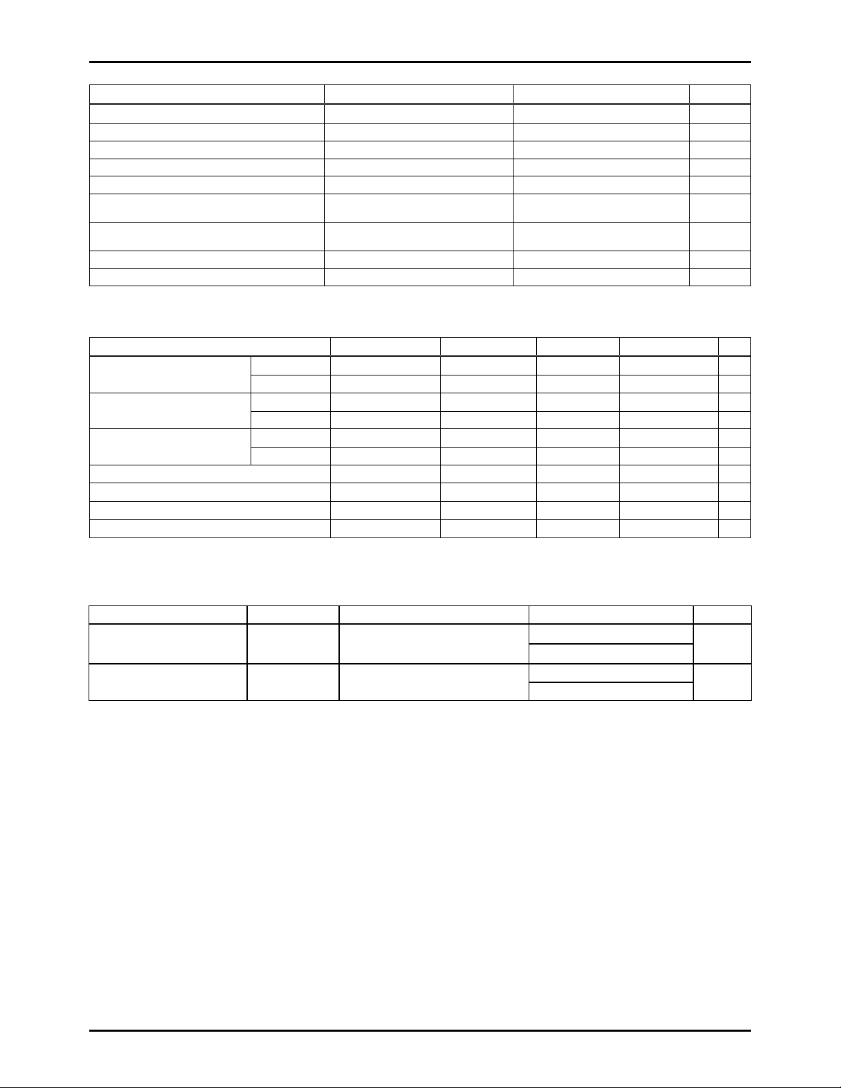
Absol ute Maxi mum Rat ings
Item Symbol Ratings Unit
H driver power supply voltage HVDD -1.0 to +14 V
V driver power supply voltage VVDD -1.0 to +14 V
Common electrode voltage VCOM -1.0 to +14 V
Driving direction signal voltage CSH, CSV -1.0 to +14 V
H driver input voltage STH, XSTH, CKH1, CKH2 -1.0 to +14 V
V driver / precharge data
input voltage
Video / precharge data
input voltage
Operating temperature (panel) Topr -10 to +60
Storage temperature Tstg -20 to +70
at VSS=0V
STV, XSTV, CKV1, CKV2,
ENB, XENB, PCG, XPCG
VG, VR, VB, VPCD -1.0 to +13 V
-1.0 to +14 V
C
°
C
°
Operating Conditions
P ower supply voltage HVDD 12.5V±0.5, VVDD 12. 5V±0.5, VSS 0V
Item Symbol MIN TYP MAX Unit
H driver input voltage
V driver input voltage
CSV, CSH
Video signal center voltage VVC T.B.D T.B.D T.B.D V
Video signal input voltage range *1 VG, VR, VB T.B.D - T.B.D V
Common electrode voltage*2 VCOM T.B.D T.B.D T.B.D V
Precharge data sign al *1 VPCD - T.B.D - V
Low VHIL -0.3 0.0 0.3 V
High VHIH 2.5 3.0 4.0 V
Low VVIL -0.3 0.0 0.3 V
High VVIH 2.5 3.0 4.0 V
Low VSIL -0.3 0.0 0.3 V
High VSIH 11.5 VDD VDD V
*1 Video signal and precharge data signal shall be input symmetrically around VVC.
*2 Set common electrode voltage to the optimum voltage.
Optical Specifications
Item Symbol Condition TYP Unit
Contrast ratio CR -30deg input
Reflection ratio - -30deg input
* Compare to standard diffusion
>=30 (max)
>=10 (0 to 50 deg)
>=40 (10 to 50 deg)
>=100 (20 to 40 deg)
-
%*
No.6773-2/8
Page 3
ALR122FNX
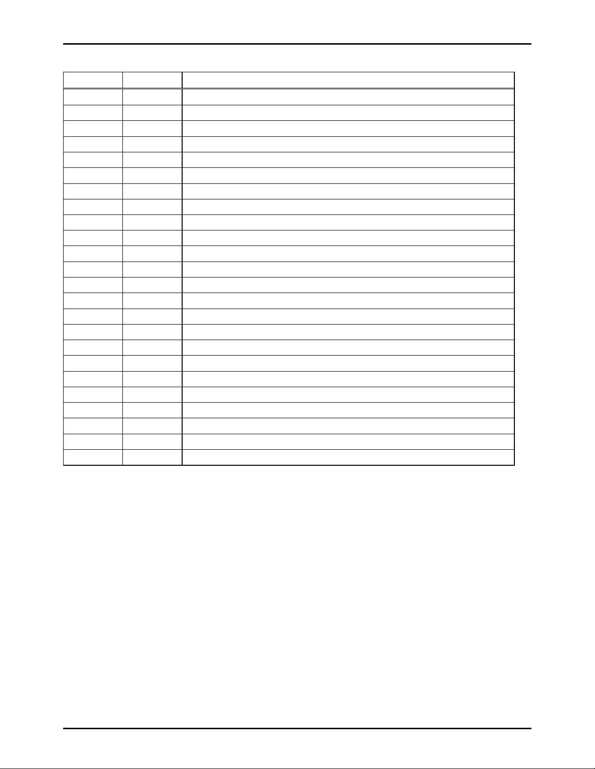
Pin Function
Pin No Symbol Function
1 NC Leave this pin open
2 COM Common electrode voltage
3 CKV1 V clock 1
4 CKV2 V clock 2
5 VVDD VDD for V drive
6 STV V start signal
7 XSTV Inverted signal of STV
8 CSV Up / down inverse control signal (H : Normal scan, L : Reverse scan)
9 ENB Enable signal
10 XENB Inverted signal of ENB
11 PCD Precharge data signal
12 B Video signal (B)
13 R Video signal (R)
14 G Video signal (G)
15 VSS VSS for V and H drive
16 XPCG Inverted signal of PCG
17 PCG Precharge gate signal
18 CSH Right / left inverse control signal (H : Normal scan, L : Reverse scan)
19 XSTH Inverted signal of STH
20 STH H start signal
21 CKH2 H clock 2
22 CKH1 H clock 1
23 HVDD VDD for H drive
24 NC Leave this pin open
No.6773-3/8
Page 4

Block Diagram
VSS
V-DRIVER
VVDD
ENB
CSV
STV
CKV2
CKV1
VSS
G
R
B
• • • • • •
Normal Scan
Reverse Scan
• • • • • •
• • • • • •
• • • • • •
ALR122FNX
Front View
H-DRIVER
Normal Scan
Reverse Scan
STH
CKH1
CKH2
HVDD
CSH
VSS
COM
VVDD
1.NC
PCD
2.COM
4.CKV2
3.CKV1
6.STV
5.VVDD
Precharege circuit
12.B
11.PCD
10.XENB
9.ENB
8.CSV
7.XSTV
13.R
14.G
16.XPCG
15.VSS
17.PCG
18.CSH
L/SL/SL/SL/SL/S
19.XSTH
20.STH
L/S
21.CKH2
PCG
XPC
G
24.NC
23.HVDD
22.CKH1
No.6773-4/8
Page 5

System Configuration
ALR122FNX
Video signal
Composite
Y/C
Y/Color
differen ce
Se ria l contro l
Video signal
Analog RGB
X'tal
processing
BUS
Sync.
sep.
Signal processing IC
Video
chroma
signal
I/F
LV4137W
R
G
B
Timing
controller
VCO
LV4135W
Signal processing IC
R
G
B
RGB
drivers
(S&H)
RGB
drivers
(S&H)
R
G
B
PCD
R
G
B
PCD
Low-temperature p-Si
TFT-LCD
Horizontal scanner
Display area
Vertical scanner
Level
shifter
Precharge circuit
ALR122
Low-temperature p-Si
TFT-LCD
Horizontal scanner
Se ria l contro l
Synchronus
signal
BUS
I/F
Sync.
sep.
Timing
controller
VCO
Vertical scanner
Level
shifter
Display area
Precharge circuit
ALR122
No.6773-5/8
Page 6

System Configuration
X'tal
Video signal
Composite
Y/C
Y/Color
differen ce
Se ria l contro l
LV4139W
Signal processing IC
**Under development
Video
chroma
signal
processing
BUS
I/F
Sync.
sep.
R
G
B
Timing
controller
ALR122FNX
RGB
drivers
(S&H)
R
G
B
PCD
Low-temperature p-Si
TFT-LCD
Horizontal scanner
Display area
Vertical scanner
Level
shifter
Precharge circuit
VCO
ALR122
No.6773-6/8
Page 7

Package Dimension
ALR122FNX
No.6773-7/8
Page 8

ALR122FNX
No.6773-8/8
PS
 Loading...