

SANYO ALP239CXX Datasheet

Ordering number : ENN6772
LCD Module
ALP239CXX
Low-Temperature Polysilicon
2.0-inch TFT LCD Module
Overview
This 2 inch low temperature poly- silicon TFT-LCD module is suitable for digital still camera or for digital video camera.
Features
• Diagonal 5.1cm (2.0inch) display size.
• 557 × 234 = 130,338 dots.
• RGB delta color arrangement.
• Operating temperature (panel) is -10 to +60°C. Ambient temperature during storage is -20 to +70°C.
• Slim design, light weight and narrow frame. (t=0.7mm glass)
• Up / down and right / left inverse function.
• Built-in level shifter circuit.
• Conform to NTSC, PAL when using recommended IC : LV4135W, LV4137W, (LV4139W : Under development)
• Anti-reflection (AR) coat.
• Panel power consumption is Typ.61mW at NTSC.
• Optical transmittance is approx. 8%.
• Low power consumption by 12V drive.
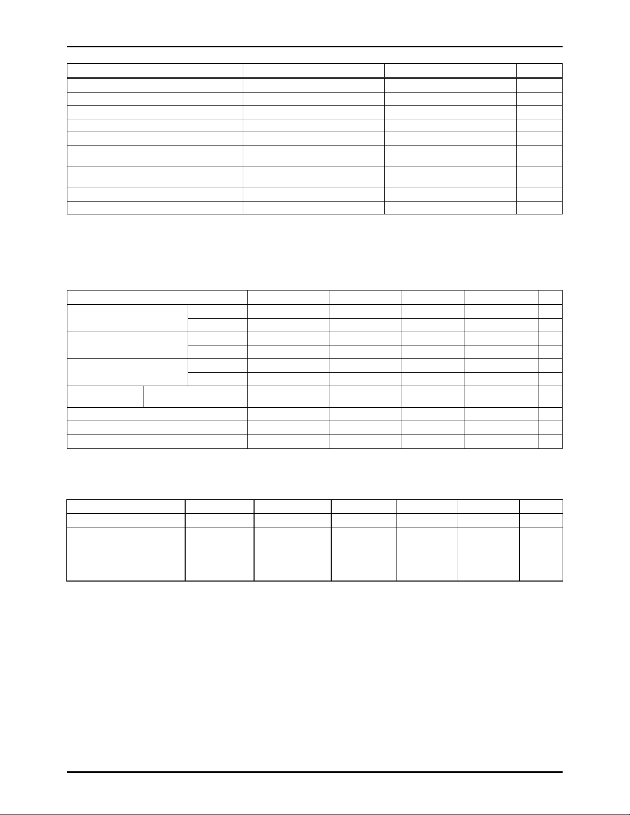
Specifications
Dot count (H) × (V) 557 × 234 dot
Effective display dimensions (H) × (V) 40.98 × 30.77 mm
Display size (diagonal) 5.1 (2.0inch) cm
Dot pitch (H) × (V) 0.0735 × 0.1315 mm
Color arrangement RGB Delta -
External Dimensions (W) × (H) × (D) TYP 47.9 × 39.9 × 2.1 mm Note1
Weight Approx. 8 g
*Note1: Excluding flexible cable and protrusions.
Item Specifications Unit Remarks
Ver.1.6
12898
13001 RM (IM) No.6772-1/8
ALP239CXX
Absolute Maximum Ratings
Item Symbol Ratings Unit
H driver power supply voltage HVDD -1.0 to +14 V
V driver power supply voltage VVDD -1.0 to +14 V
Common electrode voltage VCOM -1.0 to +14 V
Driving direction signal voltage CSH, CSV -1.0 to +14 V
H driver input voltage STH, XSTH, CKH1, CKH2 -1.0 to +14 V
V driver / precharge data
input voltage
Video / precharge data
input voltage
Operating temperature (panel) Topr -10 to +60
Storage temperature Tstg -20 to +70
at VSS=0V
STV, XSTV, CKV1, CKV2,
ENB, XENB, PCG, XPCG
VG, VR, VB, VPCD -1.0 to +13 V
-1.0 to +14 V
C
°
C
°
Operating Conditions
Power supply voltage
HVDD LV4135W LV4137W : 12.0V±0.3V
VVDD LV4135W LV4137W : 12.0V±0.3V
VSS LV4135W LV4137W : 0V
Item Symbol MIN TYP MAX Unit
H driver input voltage
V driver input voltage
CSV, CSH
Video signal
center voltage
Video signal input voltage range *1 VG, VR, VB VVC-3.5 - VVC+3.5 V
Common electrode voltage*2 VCOM (VVC-0.2)-0.2 (VVC-0.2) (VVC-0.2)+0.2 V
Precharge data signal *1 VPCD VVC±1.5 VVC±2.0 VVC±2.5 V
LV4135W, LV4137W VVC 5.0 5.2 5.4 V
Low VHIL -0.3 0.0 0.3 V
High VHIH 2.5 3.0 4.0 V
Low VVIL -0.3 0.0 0.3 V
High VVIH 2.5 3.0 4.0 V
Low VSIL -0.3 0.0 0.3 V
High VSIH 11.5 VDD VDD V
*1 Video signal and precharge data signal shall be input symmetrically around VVC.
*2 Set common electrode voltage to the optimum voltage.
Optical Specifications
Item Symbol Condition MIN TYP MAX Unit
Contrast ratio CR
θT 15
Viewing angle range
θB 35
θL 45
θR
25°C
CR >= 10 -
- 100 - -
- deg
45
No.6772-2/8
ALP239CXX
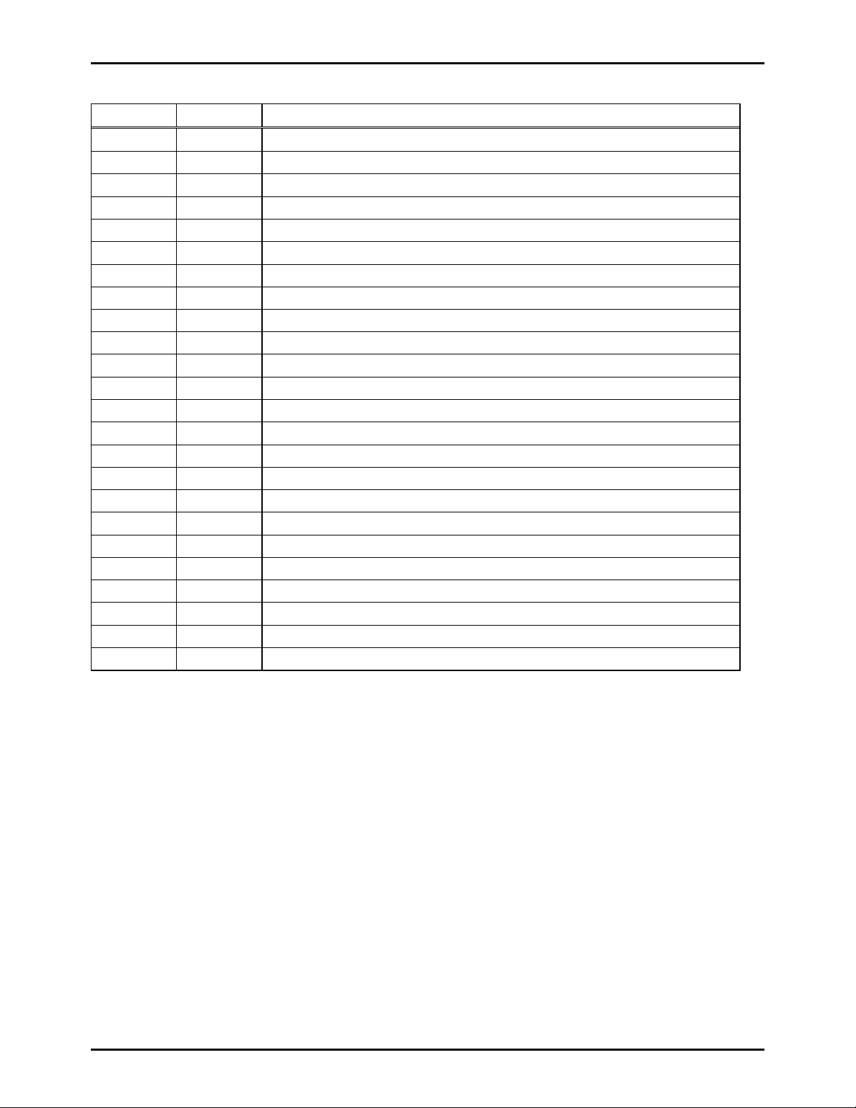
Pin Function
Pin No Symbol Function
1 NC Leave this pin open
2 COM Common electrode voltage
3 CKV1 V clock 1
4 CKV2 V clock 2
5 VVDD VDD for V drive
6 STV V start signal
7 XSTV Inverted signal of STV
8 CSV Up / down inverse control signal (H : Normal scan, L : Reverse scan)
9 ENB Enable signal
10 XENB Inverted signal of ENB
11 PCD Precharge data signal
12 B Video signal (B)
13 R Video signal (R)
14 G Video signal (G)
15 VSS VSS for V and H drive
16 XPCG Inverted signal of PCG
17 PCG Precharge gate signal
18 CSH Right / left inverse control signal (H : Normal scan, L : Reverse scan)
19 XSTH Inverted signal of STH
20 STH H start signal
21 CKH2 H clock 2
22 CKH1 H clock 1
23 HVDD VDD for H drive
24 NC Leave this pin open
No.6772-3/8
 Loading...