

Page 1
Ordering number : ENN6751A
LCD Module
ALP022AGXB
Low-Temperature Polysilicon
0.55-inch TFT LCD Module
Overview
This 0.55 inch low temperature poly- silicon TFT-LCD module consists of LCD panel and White LED backlight.
This is suitable for digital video camera or for digital still cam era as view finder.
Features
• Diagonal 1.375cm (0.55inch) display size.
• 521 × 218 = 113,578 dots.
• RGB delta color arrangement.
• Operating temperature (Panel) is -10 to +60°C. Ambient temperature during storage is -20 to +70°C.
• Slim design, light weight and narrow frame. (t=0.7mm glass)
• Builds in level shifter circuit.
• Conform to NTSC, PAL when using recommended IC : LV4135W,LV4137W, (LV4139W : Under development).
• Glare polarizer.
• Builds in White LED backlight unit. (No inverter unit.)
• Panel power consumption is Typ.27mW at NTSC. Back-light power consumption is 72mW. (reference)
• Display surface luminance is typ 130cd/m2.
Specifications
Item Specifications Unit Remarks
Dot count (H) × (V) 521 × 218 dot
Effective display dimensions (H) × (V) 11.26 × 8.37 mm
Display size (diagonal) 1.375 (0.55inch) cm
Dot pitch (H) × (V) 0.0216 × 0.0384 mm
Color arrangement RGB Delta -
External Dimensions (W) × (H) × (D) TYP 18.0 × 17.8 × 5.8 mm Note1
Weight Approx. 3 g
*Note1: Excluding flexible cable and protrusions.
Ver.1.6
12898
51001 GI IM / 13001 GI (IM) No.6751-1/9
Page 2
ALP022AGXB
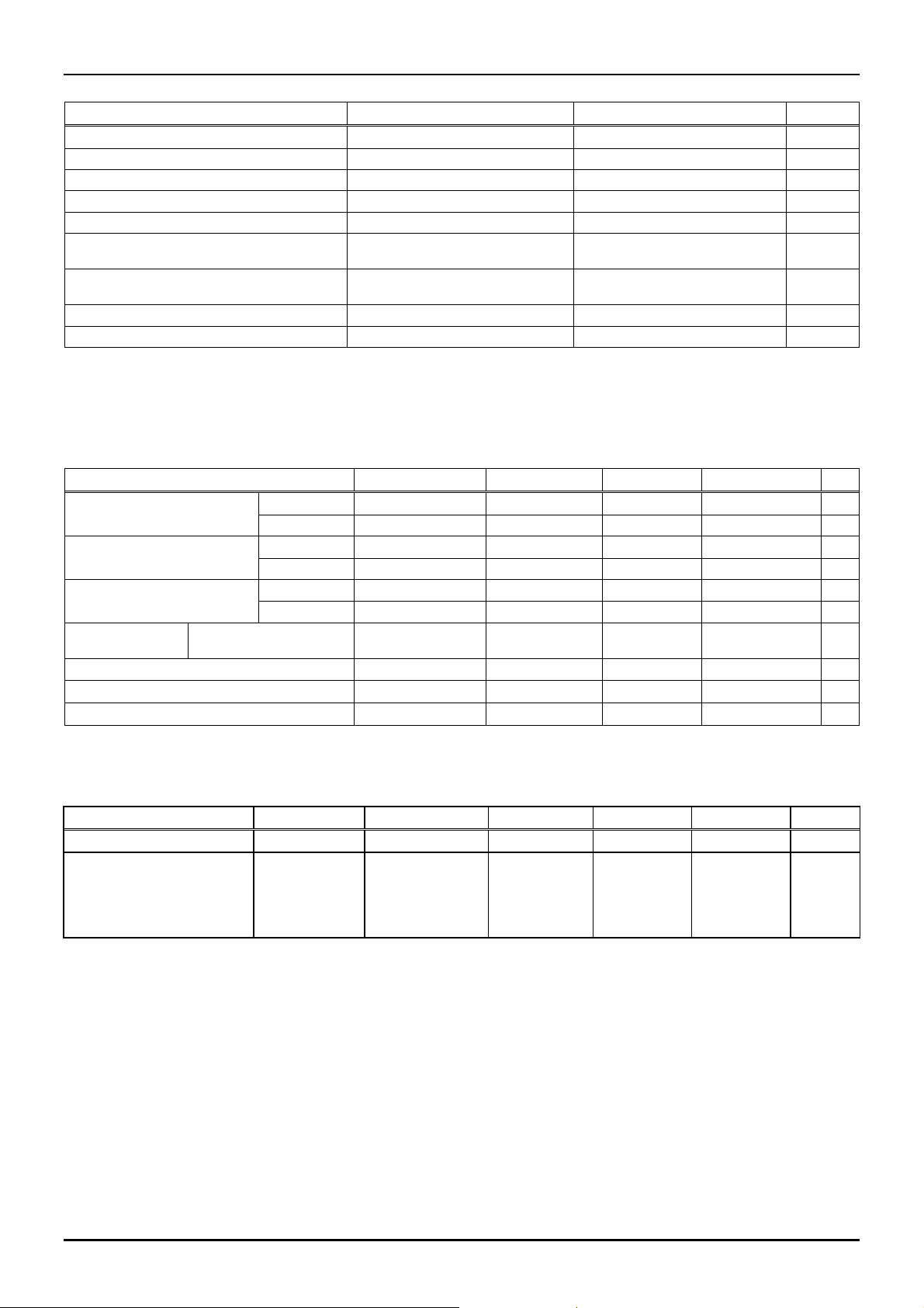
Absolute Maximum Ratings
Item Symbol Ratings Unit
H driver power supply voltage HVDD -1.0 to +14 V
V driver power supply voltage VVDD -1.0 to +14 V
Common electrode voltage VCOM -1.0 to +14 V
Driving direction signal voltage CSH, CSV -1.0 to +14 V
H driver input voltage STH, XSTH, CKH1, CKH2 -1.0 to +14 V
V driver / precharge data
input voltage
Video / precharge data
input voltage
Operating temperature (panel) Topr -10 to +60
Storage temperature Tstg -20 to +70
at VSS=0V
STV, XSTV, CKV1, CKV2,
ENB, XENB, PCG, XPCG
VG, VR, VB, VPCD -1.0 to +13 V
-1.0 to +14 V
°
C
°
C
Operating Conditions
Power supply voltage
HVDD LV4135W LV4137W : 12.0V ± 0.3V
VVDD LV4135W LV4137W : 12.0V ± 0.3V
VSS LV4135W LV4137W : 0V
Item Symbol MIN TYP MAX Unit
H driver input voltage
V driver input voltage
CSV, CSH
Video signal
center voltage
Video signal input voltage range *1 VG, VR, VB VVC-3.5 - VVC+3.5 V
Common electrode voltage*2 VCOM (VVC-0.2)-0.2 (VVC-0.2) (VVC-0.2)+0.2 V
Precharge data signal *1 VPCD VVC±1.5 VVC±2.0 VVC±2.5 V
LV4135W, LV4137W VVC 5.3 5.5 5.7 V
Low VHIL -0.3 0.0 0.3 V
High VHIH 2.5 3.0 4.0 V
Low VVIL -0.3 0.0 0.3 V
High VVIH 2.5 3.0 4.0 V
Low VSIL -0.3 0.0 0.3 V
High VSIH 11.5 VDD VDD V
*1 Video signal and precharge data signal shall be input symmetrically around VVC.
*2 Set common electrode voltage to the optimum voltage.
Optical Specifications
Item Symbol Condition MIN TYP MAX Unit
Contrast ratio CR 25°C - 100 - -
•T 15
Viewing angle range
•B 35
•L 45
•R
CR >= 10 -
- deg
45
No.6751-2/9
Page 3

ALP022AGXB
Pin Function
Pin No Symbol Function
1 COM Common electrode voltage
2 CKV1 V clock 1
3 CKV2 V clock 2
4 VVDD VDD for V drive
5 STV V start signal
6 XSTV Inverted signal of STV
7 CSV Up / down inverse control signal (H : Normal scan, L : Reverse scan)
8 ENB Enable signal
9 XENB Inverted signal of ENB
10 PCD Precharge data signal
11 B Video signal (B)
12 R Video signal (R)
13 G Video signal (G)
14 VSS VSS for V and H drive
15 XPCG Inverted signal of PCG
16 PCG Precharge gate signal
17 CSH Right / left inverse control signal (H : Normal scan, L : Reverse scan)
18 XSTH Inverted signal of STH
19 STH H start signal
20 CKH2 H clock 2
21 CKH1 H clock 1
22 HVDD VDD for H drive
No.6751-3/9
Page 4

Block Diagram
VSS
ALP022AGXB
Rear View
Normal Scan
Reverse Scan
STH
CKH1
VSS
G
R
B
H-DRIVER
......
CKH2
HVDD
CSH
VSS
COM
VVDD
CKV1
CKV2
STV
V-DRIVER
VVDD
ENB
CSV
Normal Scan
...
Reverse Scan
...
...
PCD
4.VVDD
3.C KV2
2.C KV1
1.C OM
...
...
...
PCG
L/S
20.CKH2
21.CKH1
XPCG
22.HVDD
PRECHARGE CIRCUIT
L/SL/SL/SL/SL/S
19.STH
18.XSTH
17.CSH
16.PCG
15.XPCG
14.VSS
13.G
12.R
11.B
10.PCD
9.XENB
8.E NB
7.C SV
6.X S TV
5.S TV
No.6751-4/9
Page 5

System Configuration
ALP022AGXB
Video signal
Com posite
Y/C
Y/C o lo r
diffe re n c e
Serial control
Video signal
Analog RGB
X'tal
Video
chroma
signal
processing
BUS
I/F
Sync.
sep.
LV4137W
Signal processing IC
R
G
B
Timing
controller
VCO
LV4135W
Signal processing IC
R
G
B
RGB
drivers
(S&H)
RGB
drivers
(S&H)
R
G
B
PCD
R
G
B
PCD
Low -temperature p-Si
TFT-LCD
Horizontal scanner
Display area
Vertical scanner
Level
shifter
Precharge circuit
ALP022
Low -temperature p-Si
TFT-LCD
Horizontal scanner
Display area
Serial control
Synchronus
signal
BUS
I/F
Sync.
sep.
Timing
controller
VCO
Vertical scanner
Level
shifter
Precharge circuit
ALP022
No.6751-5/9
Page 6

System Configuration
Video signal
Com posite
Y/C
Y/Color
differen c e
Serial control
X'tal
processing
BUS
Sync.
sep.
ALP022AGXB
LV4139W
Signal processing IC
**Under developm ent
Video
chroma
signal
I/F
R
G
drivers
B
(S& H )
Timing
controller
RGB
R
G
B
PCD
Low -temperature p-Si
TFT-LCD
Horizontal scanner
Display area
Vertical scanner
Level
shifter
Precharge circuit
1c h ip dr ive (EVF & T N L CD)
LV4137W /LV4139W
Video signal
X'tal
Composite
Y/C
Y/Color
differen c e
Serial control
Signal processing IC
Video
chroma
signal
processing
BUS
I/F
Sync.
sep.
VCO
R
G
drivers
B
(S&H)
Timing
controller
RGB
ALP022
Low -temperature p-Si
TFT-LCD
Monitor
LCD
ALP121/ALP228/
ALP230/ALP239/ALP236
EVF LCD
VCO
*Note that the monitor LCD and the EVF LCD cannot be
driven at the same time.
ALP022
No.6751-6/9
Page 7

System Configuration
1ch ip d r iv e (EVF & T N o r S u r v ival® LCD)
Video signal
Com posite
Y/C
Y/C o lor
differe n c e
X'tal
processing
ALP022AGXB
LV4139W
Signal processing IC
**Under development
Video
chroma
signal
R
RGB
G
drivers
B
(S&H)
Low-temperature p-Si
TFT-LCD
Monitor
LCD
ALP237/ALP233/ALP234
Serial control
2chip drive (EVF & Survival® LCD)
Video signal
Com posite
Y/C
Y/C o lor
differe n c e
Serial control
BUS
I/F
Sync.
sep.
X'tal
LV4131W
processing IC
controller
Signal
Timing
VCO
EVF LCD
ALP022
Low-temperature p-Si
TFT-LCD
Monitor
LCD
VCO
ALP237/ALP233/ALP234
X'tal
LV4137W
Signal
processing IC
EVF LCD
ALP022
No.6751-7/9
Page 8

Package Dimension
ALP022AGXB
No.6751-8/9
Page 9

ALP022AGXB
No.6751-9/9
PS
 Loading...