

SANYO 2SC3446 Datasheet
SANYO Electric Co.,Ltd. Semiconductor Bussiness Headquaters
TOKYO OFFICE Tokyo Bldg., 1-10, 1 Chome, Ueno, Taito-ku, TOKYO, 110-8534 JAPAN
Any and all SANYO products described or contained herein do not have specifications that can handle
applications that require extremely high levels of reliability, such as life-support systems, aircraft’s
control systems, or other applications whose failure can be reasonably expected to result in serious
physical and/or material damage. Consult with your SANYO representative nearest you before using
any SANYO products described or contained herein in such applications.
SANYO assumes no responsibility for equipment failures that result from using products at values that
exceed, even momentarily, rated values (such as maximum ratings, operating condition ranges,or other
parameters) listed in products specifications of any and all SANYO products described or contained
herein.
NPN Triple Diffused Planar Silicon Transistor
500V/3A Switching Regulator Applications
Ordering number:EN1544B
2SC3446
Features
· High breakdown voltage and high reliability.
· Fast switching speed (tf : 0.1µs typ).
· Wide ASO.
· Adoption of MBIT process.
Specifications
Absolute Maximum Ratings at Ta = 25˚C
retemaraPlobmySsnoitidnoCsgnitaRtinU
egatloVesaB-ot-rotcelloCV
egatloVrettimE-ot-rotcelloCV
egatloVesaB-ot-rettimEV
tnerruCrotcelloCI
)esluP(tnerruCrotcelloCI
tnerruCesaBI
noitapissiDrotcelloCP
erutarepmeTnoitcnuJjT 051
erutarepmeTegarotSgtsT 051+ot55–
Electrical Characteristics at Ta = 25˚C
retemaraPlobmySsnoitidnoC
tnerruCffotuCrotcelloCI
tnerruCffotuCrettimEI
niaGtnerruCCD
tcudorPhtdiwdnaB-niaGf
ecnaticapaCtuptuOC
* : The hFE1 of the 2SC3446 is classified as follows. When specifying the hFE1 rank, specify two ranks or more in principle.
03L5104M0205N03
OBC
OEC
OBE
C
PW≤300µs, Duty Cycle≤10%
PC
B
Tc=25˚C
C
V
OBC
OBE
hEF1VECI,V5=
hEF2VECI,V5=
T
bo
BC
V
BE
V
EC
V
BC
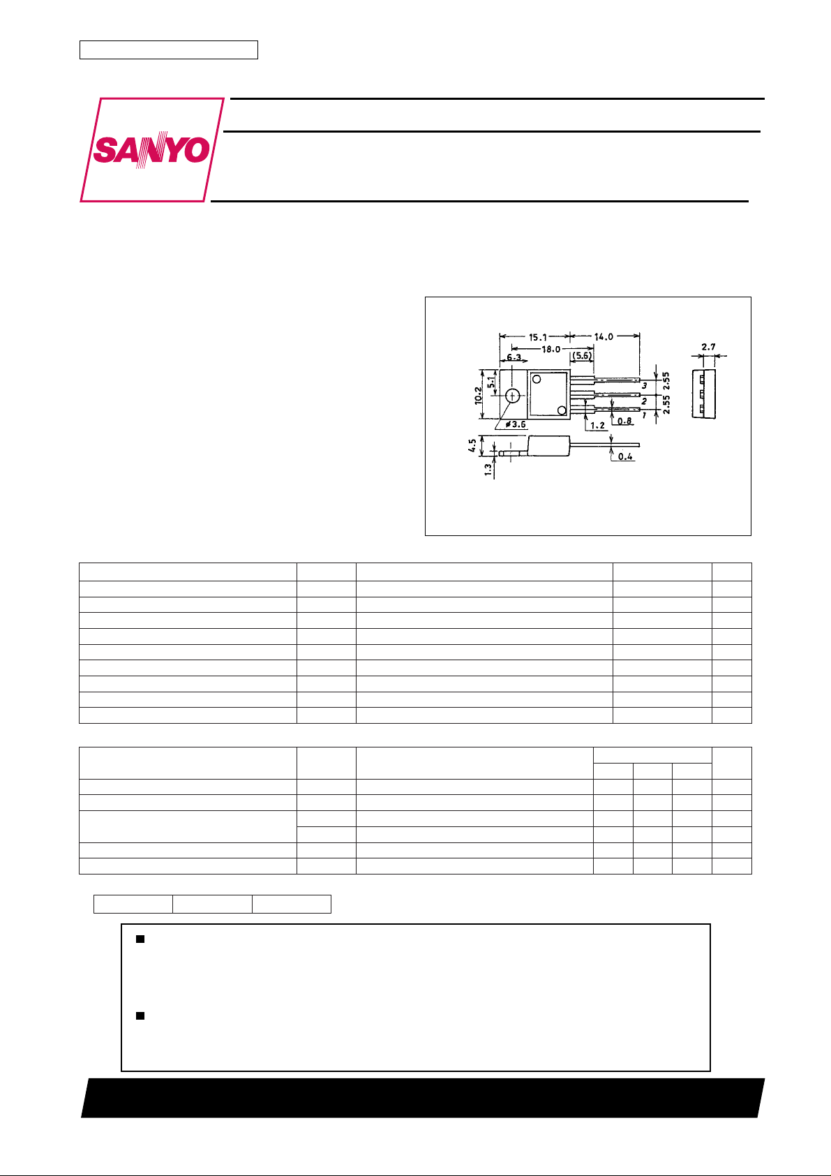
Package Dimensions
unit:mm
2010C
[2SC3446]
JEDEC : T O-220AB
EIAJ : SC-46
nimpytxam
I,V005=
0=01Aµ
E
I,V5=
0=01Aµ
C
A3.0=
C
A5.1=
C
I,V01=
A3.0=
C
zHM1=f,V01=
*51
8
1 : Base
2 : Collector
3 : Emitter
008V
005V
7V
3A
6A
1A
04W
sgnitaR
81zHM
05Fp
˚C
˚C
tinU
N1098HA (KT)/4217KI/3085KI/6154KI, MT No.1544–1/4
2SC3446
retemaraPlobmySsnoitidnoC
egatloVnoitarutaSrettimE-ot-rotcelloCV
egatloVnoitarutaSrettimE-ot-esaBV
egatloVnwodkaerBesaB-ot-rotcelloCV
egatloVnwodkaerBrettimE-ot-rotcelloCV
egatloVnwodkaerBesaB-ot-rettimEV
egatloVniatsuSrettimE-ot-rotcelloCV
emiTNO-nruTt
emiTegarotSt
emiTllaFt
I
I,A5.1=
)tas(EC
C
I
C
)tas(EB
I
OBC)RB(
C
I
OEC)RB(
C
I
OBE)RB(
E
I
)sus(XEC
C
V
no
gts
f
CC
V
CC
V
CC
A3.0=
B
I,A5.1=
A3.0=
B
I,Am1=
0=008V
E
R,Am5=
=∞ 005V
EB
I,Am1=
0=7V
C
I,A5.1=
I–=
1B
2B
I5,V002=
I5.2–=
1B
I5,V002=
I5,V002=
2BI=C
I5.2–=
1B
2BI=C
I5.2–=
1B
2BI=C
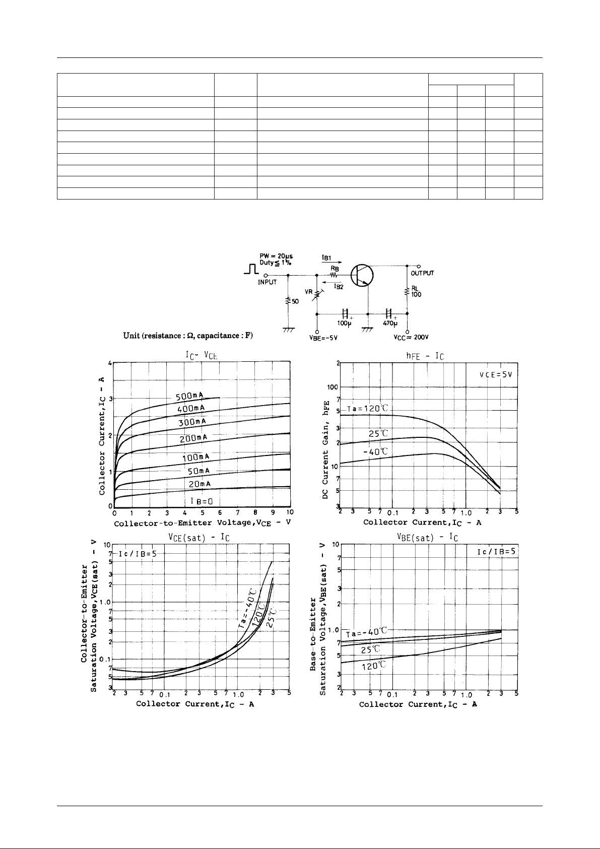
Switching Time Test Circuit
sgnitaR
nimpytxam
depmalc,Hm2=L,A6.0=005V
R,A2=
001= Ω
L
R,A2=
001= Ω
L
R,A2=
001= Ω
L
tinU
0.1V
5.1V
5.0sµ
0.3sµ
3.0sµ
No.1544–2/4
 Loading...