

SANYO 2SC3142 Datasheet
SANYO Electric Co.,Ltd. Semiconductor Bussiness Headquaters
TOKYO OFFICE Tokyo Bldg., 1-10, 1 Chome, Ueno, Taito-ku, TOKYO, 110-8534 JAPAN
Any and all SANYO products described or contained herein do not have specifications that can handle
applications that require extremely high levels of reliability, such as life-support systems, aircraft’s
control systems, or other applications whose failure can be reasonably expected to result in serious
physical and/or material damage. Consult with your SANYO representative nearest you before using
any SANYO products described or contained herein in such applications.
SANYO assumes no responsibility for equipment failures that result from using products at values that
exceed, even momentarily, rated values (such as maximum ratings, operating condition ranges,or other
parameters) listed in products specifications of any and all SANYO products described or contained
herein.
NPN Epitaxial Planar Silicon Transistor
High-Frequency
General-Purpose Amplifier Applications
Ordering number:EN1066A
2SC3142
Features
· FBET series.
· Compact package enabling compactness of sets.
· High fT and small cre (fT=750MHz typ, cre=0.6 typ).
Specifications
Absolute Maximum Ratings at Ta = 25˚C
retemaraPlobmySsnoitidnoCsgnitaRtinU
egatloVesaB-ot-rotcelloCV
egatloVrettimE-ot-rotcelloCV
egatloVesaB-ot-rettimEV
tnerruCrotcelloCI
noitapissiDrotcelloCP
erutarepmeTnoitcnuJjT 521
erutarepmeTegarotSgtsT 521+ot04–
Electrical Characteristics at Ta = 25˚C
retemaraPlobmySsnoitidnoC
tnerruCffotuCrotcelloCI
tnerruCffotuCrettimEI
niaGtnerruCCD
tcudorPhtdiwdnaB-niaGf
ecnaticapaCkcabdeeFC
tnatsnoCemiTrotcelloC-ot-esaBr
erugiFesioNFNVECI,V6=
niaGrewoPGPVECI,V6=
* : The 2SC3142 are classified as follows according to hFE at 1mA :
(Note) Marking : J
hFE rank : 2, 3, 4
C
h
T
bbC'C
OBC
OEC
OBE
C
V
OBC
V
OBE
V
EF
V
V
er
V
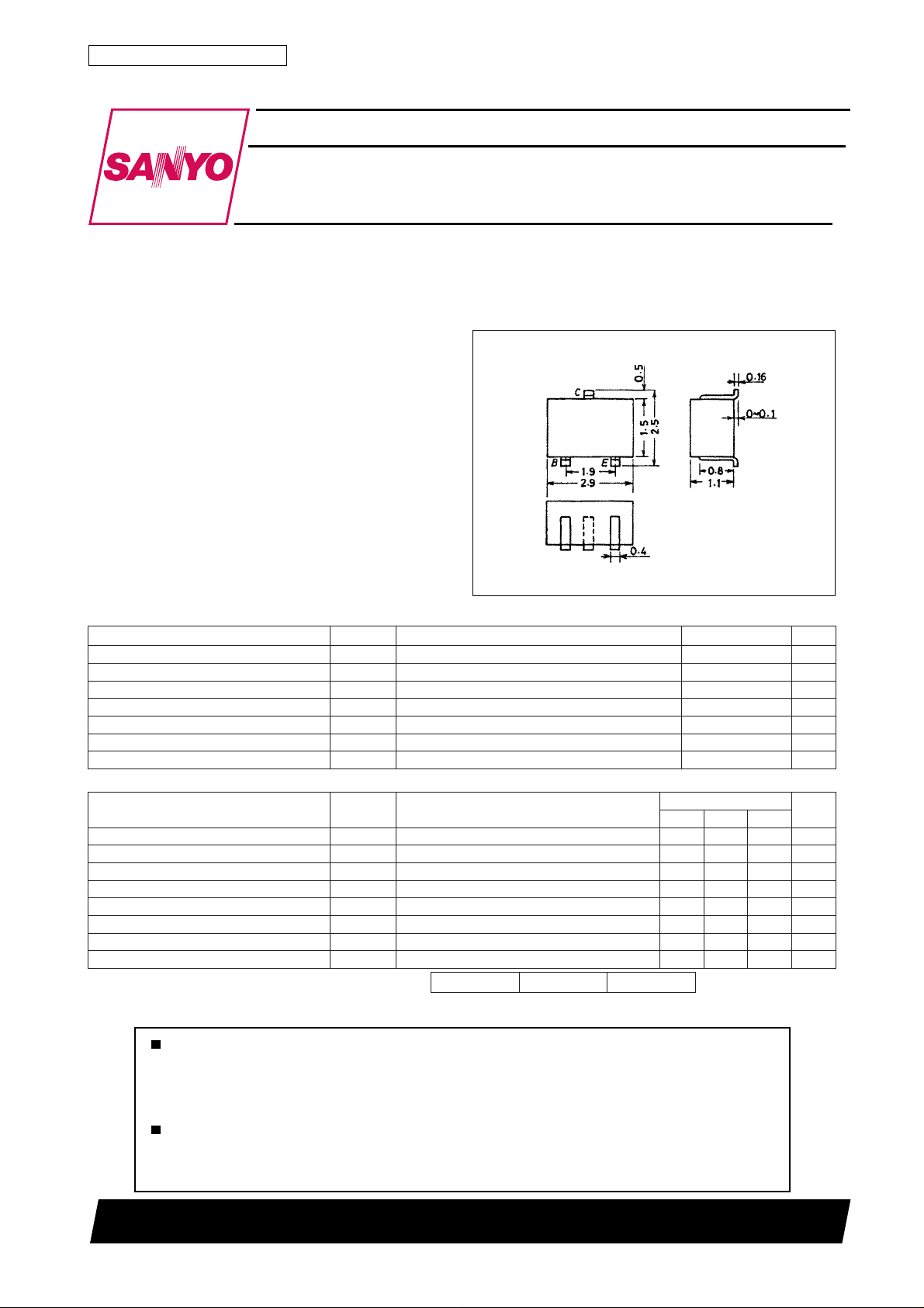
Package Dimensions
unit:mm
2018A
[2SC3142]
C : Collector
B : Base
E : Emitter
SANYO : CP
52V
02V
3V
03Am
051Wm
˚C
˚C
sgnitaR
nimpytxam
I,V01=
BC
BE
EC
EC
BC
EC
0=1.0Aµ
E
I,V3=
0=1.0Aµ
C
I,V6=
Am1=
C
I,V6=
Am4=
C
zHM1=f,V6=
I,V6=
C
C
C
zHM9.13=f,Am1=91sp
zHM001=f,Am1=
zHM001=f,Am1=
08204021306081409
*04*081
054057zHM
6.09.0Fp
2.2Bd
82Bd
tinU
O3098HA (KT)/4207KI/8192KI, TS No.1066–1/5
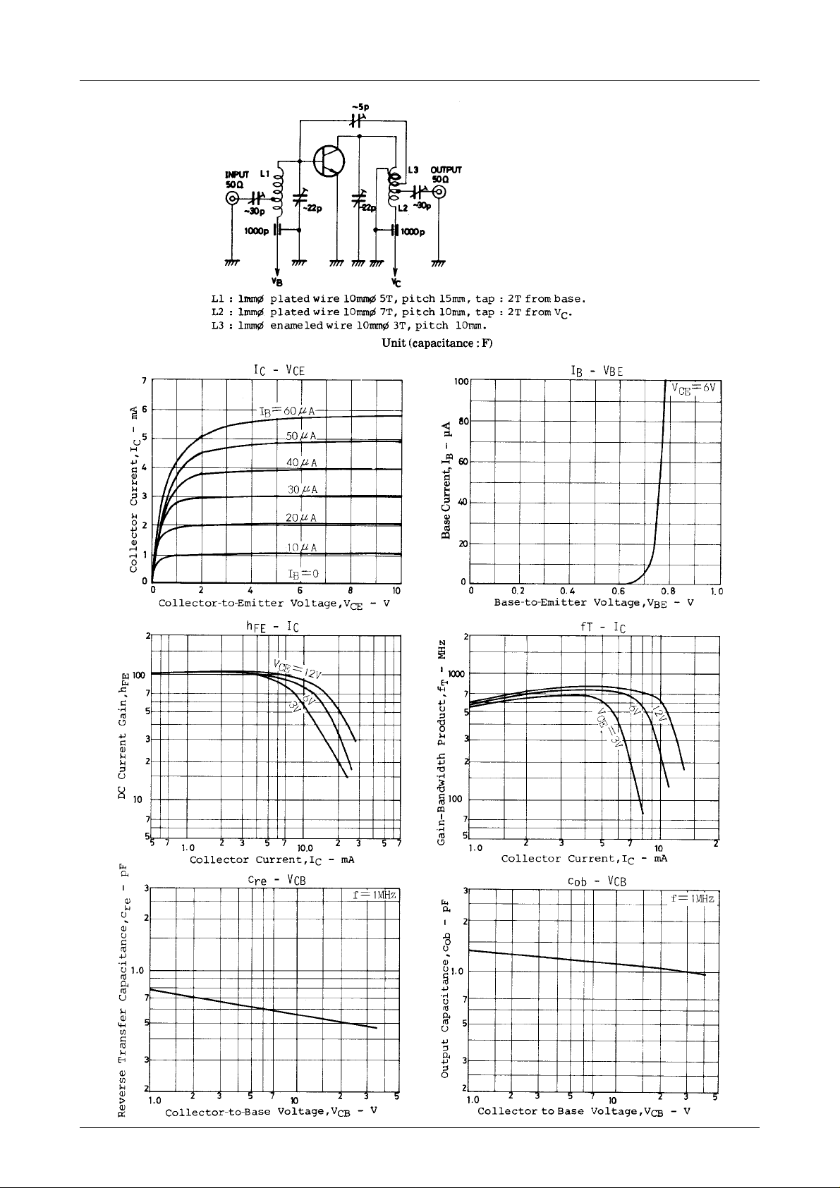
NF, PG Test Circuit
2SC3142
No.1066–2/5
 Loading...