

Page 1
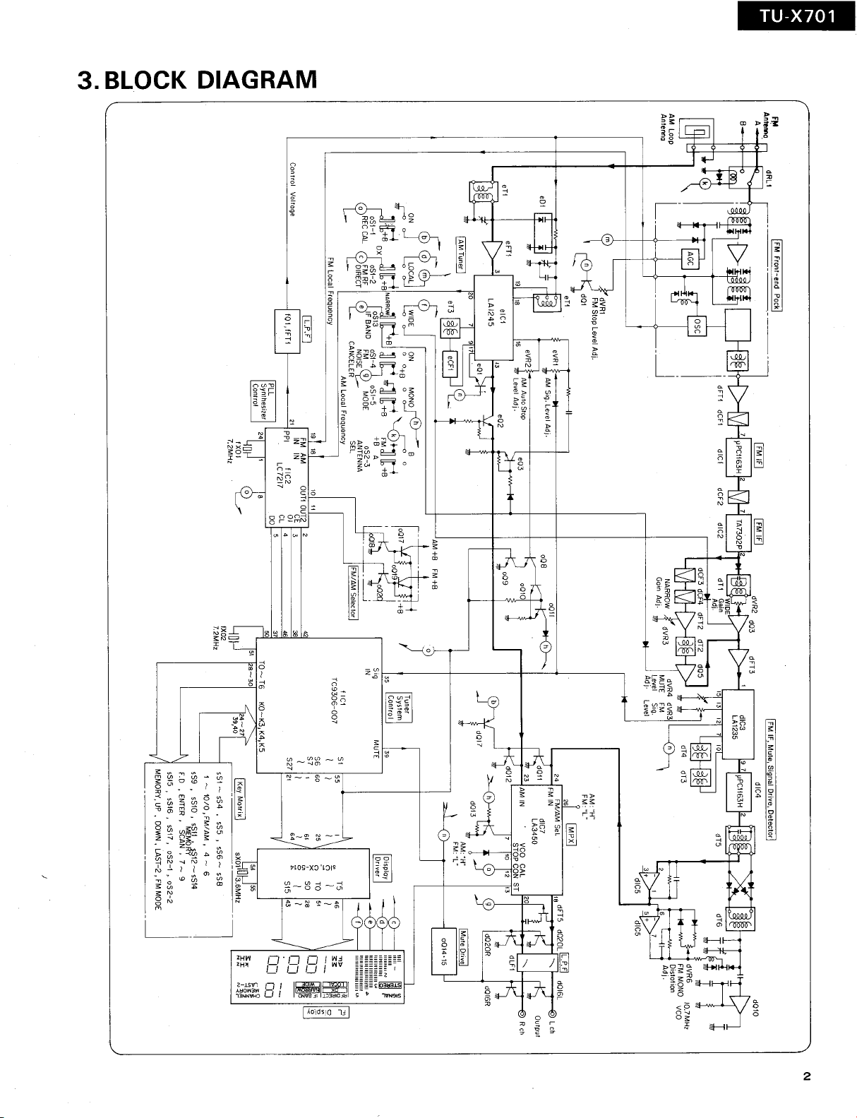
Page 2
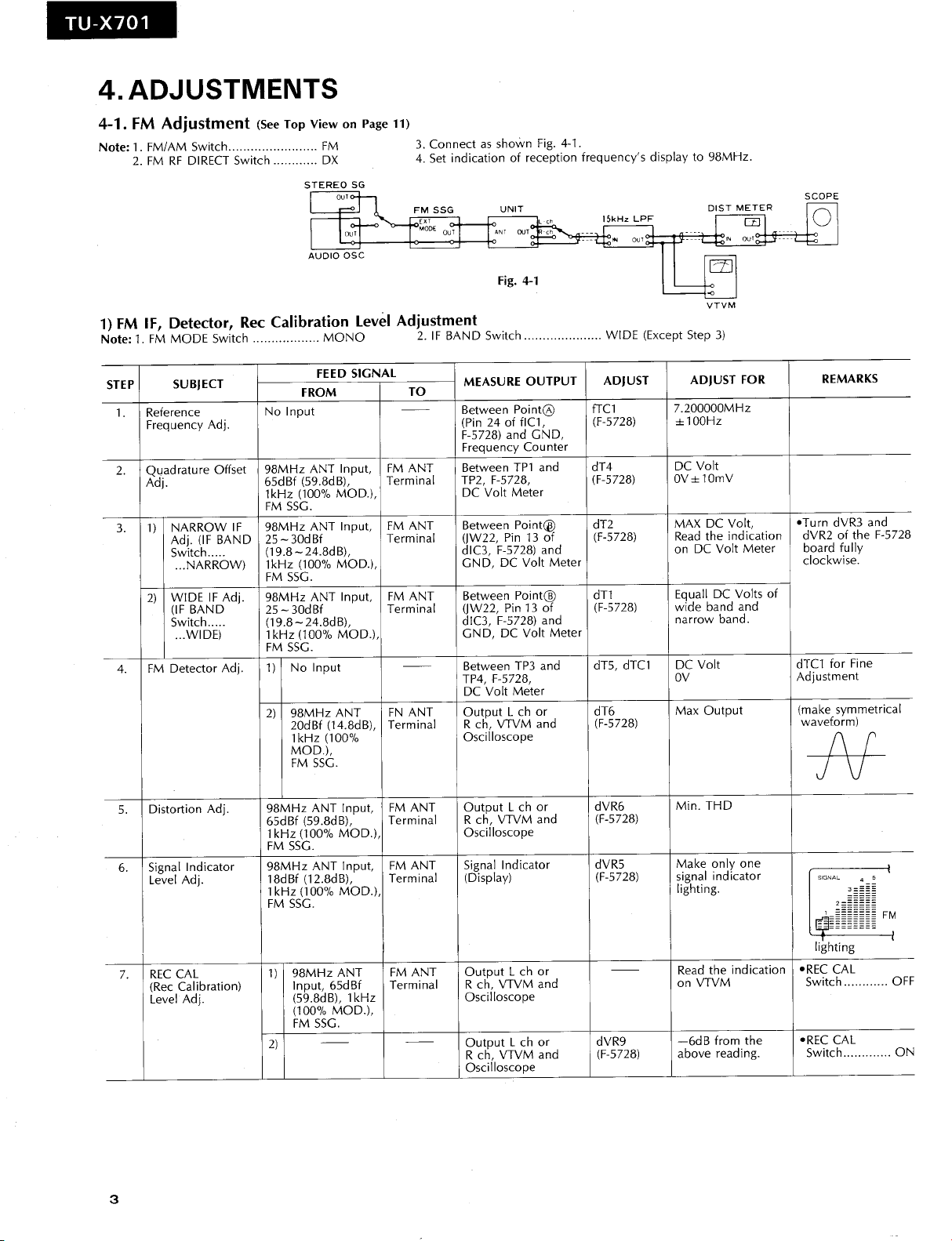
Page 3
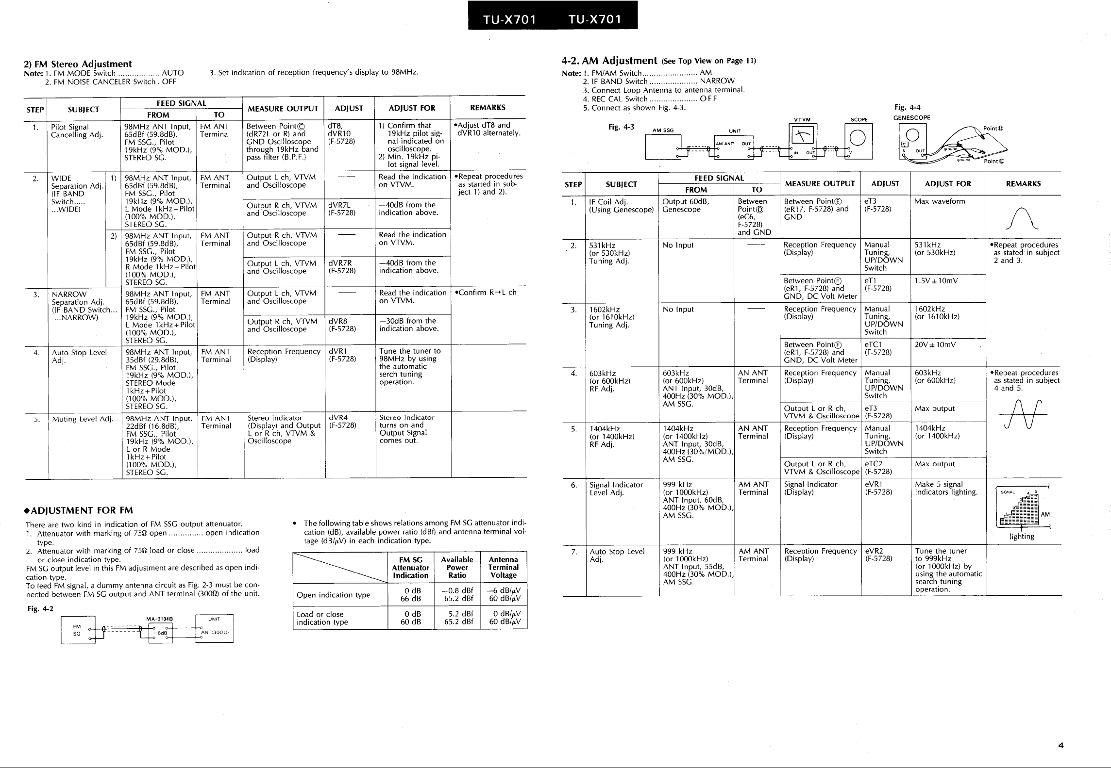
Page 4
Page 5
Page 6

Page 7

Page 8

Page 9

Page 10

Page 11

Page 12

Page 13

Page 14

Page 15

Page 16

..::::
..::::
::;;
'-'
~"' ",.. """
;,:
;::~~
'" .. ~ ~ ~
TU-
X701 TU-
X701
~~
::;
~~ ~~ ~
~~ ~ ~~ ~
~~ ~~ ~
~ '"
~~;~
10. DESCRIPTION OF ICs,
-TC9306-
REF
iNT
iNH
TEST
Xl'
GND
VDD
COM2
. TC9306-007
Pin No.
1- 21 S7-
55-
007
o",~
(f)(f)U(f)
45 44 43 42 41 40 39
Serial
Interface
.54
(f)(f)
Pin Name
COM1
COM2
S1-
Digital Tuning System
w Z
C( -
0 6
.. ;:: N
;;;~2
(f)
(f) (f) (f) (f)
Terminal
Terminal for outputting common signals to FL
display driver IC.
Note: The output is
Terminals for outputting segment signals to FL
S27
display driver IC. A control of a maximum of
54 segments is possible on the basis of matrix
with COM1 and COM2,
through these terminals when SEG instruction
(COM1 system) or MARK instruction (COM2
system) is executed.
Note:
N M M '"
Q.Q.
Q.Q.~
I/O Port
Driver
(f) (f) (f) (f)
Function;:::.
ically when the system is reset or ex-
ecuting CK STP instruction.
The output is fixed at "
the system is reset or excuting CK STP
instruction.
Control;:::.
26
25
,::! 24
~"'m
(f) (f) (f)
Function
fixed at " L" level automat-
(f)
Data are outputted
L" level when
TC9306 AND CXP5014
Pin No.
24-
28 - 34 TO - T6
VDD
COM1
S27
S26
S25
S24
S23
S22
Pin Name Function
KO-
AID IN
DC.REF built-in AID converter. The built-
MUTE A port for outputting a mute control signal.
Ports for inputting a 4-bit key matrix signal.
On the other hand, key return timing signals
are outputted from output ports TO to T6.
Ports for outputting key matrix return timing
signals. A 4-
T3, while a 3-bit signal is outputted from T4
to T6.
bit signal is outputted from TO to
Terminals for inputting analog signals to 4-bit
verter is of successive comparison type in de-
pendence upon program, A reference voltage
is inputted through DC.REF and an analog con-
parison voltage is inputted through AID IN.
Note: This output~et to "L" level automat-
ically when INH input changes from "
to "L" or vice versa.
STB
INT Terminal for
TEST Terminal for inputting a test mode control sig-
GND
VDD Terminal for applying a device supply voltage.
Serial interfaces fo.r STB (strobe pulse output)
LC7217, CK (serial clock output), SO (serial
data output), and SI
LC7217 PLL IC is controlled by executing SIO
instruction,
Terminal for outputting a reference frequency
signal supplied to LC7217 PLL
Note: This output is
matically when INH input is at "
inputting~ystem resetting sig-
nal to device. When INT is at "
device is reset; when at "
starts beginning from address No,
minal is usually fixed at "H" level , because the
device is reset when a voltage of 4.
plied to VDD. (power-on reset)
nal. The device is returned to the ordinary
operation at "
terminal includes a pull-
fixed at " L" level usually.
Terminals for connecting a quartz oscillator of
7.4 MHz.
GND Terminal
In the normal operation, a voltage of 5V", 1 0%
is applied; but in back-up condition
tage can be reduced to 2V.
voltage of 4.5V is applied to this terminal, the
device is reset and then program starts begin-
ning from address No.
L" level or in NC status. This
in AID con-
(serial data input),
fixed at " L" level auto-
IC.
H" level
L" level.
L" level, the
, program
O. This ter-
5V is ap-
down resistor and is
, the vol-
Further, when a
O (power-on reset).
11 . INTERIOR BLOCK DIAGRAM OF
-LC3450 (MPX)
"0
1ij~ ~ :i'
-TA7302P (FM IF Amp.
jlPC1163H (FM IF Amp.
~~ s~ ~~ ~~
6 ~~ ~
6 ~5 5~ 58
~~ d ~~
-LA1245 (AM Tuner)
"'6
l01
- LC7217 (PLL Synthesizer)
XDUT
-LA1235 (IF Amp.
S. Metee
ICs
OUTD OUT! OUT2 OUT3 OUT. OUTS OUT6
.Detector.Muting.
Signal Meter Drive)
vcc
POl
PD2
LCTR
INO INI
7 )~U
-NjM2043D (OP Amp.
-CXP5014 ..:::: FL Display
~O
N_O
xxxoz'-'w'-"-'x
Q.Q.Q.'-'~ZC(Zzwxo~
~&J~;;:~;nU~g(j)~~U\
Q.Q.Q.Q.Q.
Driver;:::.
~-'r':~
. CXP5014
Pin No.
62-
26,
28 - 43 S1-S15
46-
PX3, PDO-
PCO- 3, PFO-
PEO- 3, PBO-
PAO-
PXO-
COM2
VDD
GND
T5 - TO
VFDP
DUTY
, XT
RESET
COM1
..::::Terminal Function;:::'
Pin Name
ilO
Terminal for inputting a FL display indicator
driving signals.
Terminal for inputting common signal for FL
display.
Terminals for applying a device supply
voltage.
GND Terminal
Terminals for outputting segment signals to
FL display.
Terminals for outputting grid signals to FL
display,
Terminal for connecting a supply voltage (-
to filament of FL display.
Terminal for setting a display mode for FL
display.
Norminally this terminal is kept in "
Terminal for connecting a quartz oscillator
of 3. 6 MHz.
Terminal for inputting a reset signal.
Terminal for inputting common signal for FL
display.
Description
L" level.
SAN SUI
I ) Vcc
SANSUI ELECTRIC CO" LTD,
SANSUI ELECTRONICS CORPORATION:
SAN SUI ELECTRONICS (U, I LTD,
SANSUI ELECTRONICS G,
LlJ7./(~5tltt~~t.t
14- , Izumi 2-chome, Suginami-
PHONE: (03! 324-8891 /TELEX: 232-
1250 Valley Brook Ave, Lyndhurst, N,
17150 South Margay Ave, Carson, Calitornia 90746 U,
3036 Koapaka Street, Honolulu
Unit 10A, Lyon Industrial Estate
Paul Ehrich Strasse 8, 6074 Rodermark 2
HE~i*J,&~J11) -It-I:::
(SM2-
:AHtjjtJ11) **'l:B=liImT~if8-
Printed in Japan (1987,
ku, Tokyo 168 japan
, Hawaii 96819 U.
, Rockware Avenue, Greenford, Middx U86, OAA, England
A-OUT I
V- 4
20.76 IInternational Division!
j, 07071 U,
, West Germany
9-16(T18l) ~,i'i0422-46-8131
07, M) ~Stock No, 36531500)0
v +
z.. B - OUT
6 B- IN
5 B+IN
Top View
 Loading...