

Page 1
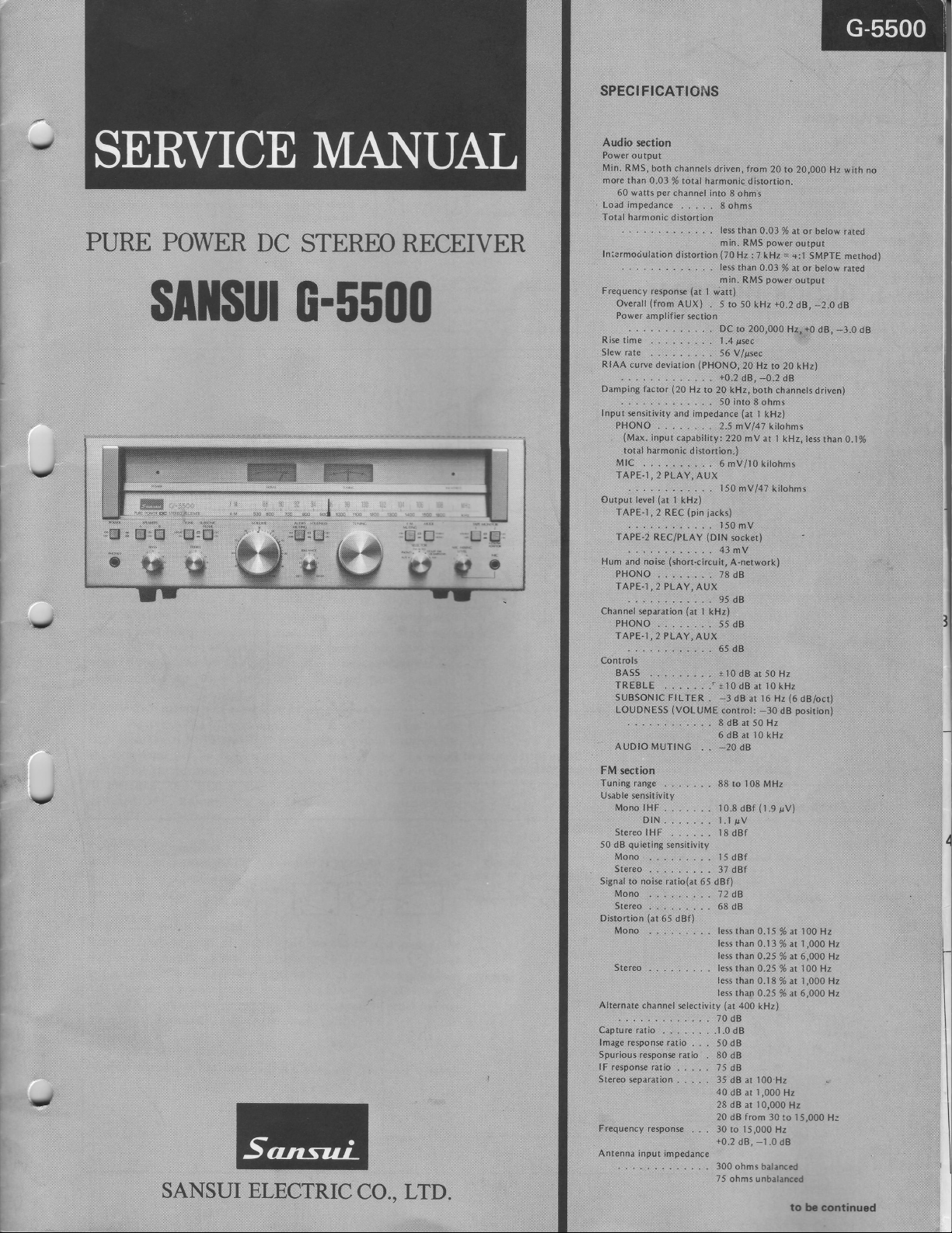
PURE POWER
DC
$]t$ul
SANSUI
ELECTRIC
STEREO RECEIVER
g-5500
CO.,
LTD.
SPECI
FICATIOi.JS
Audio
section
Power output
Min.
RMS,
more than
Load
Total
Inicrmociulation
Frequency
R
Slewrate
RIAA
Damping
lnput
Output level
Hum and noise
Channel sepdrarion
Controls
FM
Tuning range
Usable sensitivity
50 dB
Signal
Distortion
Alternate
Captureratio
lmage response
Spurious response
lF response ratio
Stereo separation
Frequency
Antenna input impedance
both channels
0.03 % total
per
60 watts
Overall
Power
jse
time
PHONO
(Max.
total harmonic
MtC
TAPE-I,2
TAPE-1,
TAPE-2 REC/PLAY
PHONO
TAPE-I,
PHONO
TAPE.I,
BASS
TREBLE
SUBSONIC FILTER
LOUDNESS
AUDIO
impedance
harmonic
response
(from
amplifier
curve
deviarion
factor
sensirivity
input
PLAY,
(at
REC
2
{short-circuit,
2
PLAY,
2 PLAY,
MUTING
channel
distortion
disrortion
AUX)
(20
and impedance
capability:
1
kHz)
(VOLUME
section
Mono ll-lF
DIN..
Stereo ll{F
quie
ting sensitivity
Mono
Stereo
noise ratio(at
to
*i.1
Mono
Srereo
65 dBf
{at
channel
ratio
response
:
selectiviry
. . . . .
ratio
. . . 35
. less than
. less
(at
section
....
(PHONO,
.
Hz
... 50into8ohms
...2.5mV/4Tkitohms
distortion.)
AUX
(pin jacks)
...78d8
AUX
{at
...ssdB
AUX
)
.. 70dB
. . 50dB
. . . 75
.
. .
driven, from
harmonic
into 8
8 ohms
min. RMS
{70
min. RMS
I
watt)
5 to
. . DC
I.4
56V/gsec
+0.2
to
20
6 mV/10
t50mV
..
{DlN
4JmV
.
.. 95dB
I kHz)
.. 65dB
,,
.i i l0
-3
.
conrrol:
.. 8dBat50Hz
6dBari0kHz
_20
. .
88 to
10.8dBf
1.1
rSdBf
l5
J7
65
dBf)
72
68
less
less
tess
tess than
less
less
.l.0dB
80
40
28 dB ar 10,000
20 dB from
l0 ro 15,000
+0.2d8,
300
75
20 to 20,000
distortion.
ohms
0.03
power
Hz :7 LHz
than
0.03 % at
power
S0
kHz
200,000
ro
psec
20 Hz
to 20 kHz)
-0.2
dB,
kHz,
both channels
(at
1 kHz)
220
mV at I
kilohms
socker)
A-network)
10 dB
at 50
dB ar 10 kHz
dB
16
dt
-10
dB
108 MHz
{lepV}
pV
dBf
dBf
dB
dB
than
0.1-5
than 0.13 % at. 1
than O.2S
0.25 % at 100
than
A.18
than
0.25
(at
400
kHz)
dB
dB
100
dB ar
I
dB ar
,000
30 ro 15,000
10dB
ohms
hal.tncei
ohms unbd,i''i;cc
Hz
at
%
or below rated
output
=
+:l
SMpTE method)
or
below
output
-2.0
+0.2
dB,
+6
Hz,
69,
dB
driven)
tess
kHz,
than 0.'l%
Hz
(6
HL
dBlocr)
position)
dB
at
100
7o
Hz
Hz
,000
o/o
at 6,000
Hz
Hz
1,000
at
Hz
at
Hz
6,000
Hz
Hz
H:
%
%
Hz
Hz
to be continued
wirh
rated
dB
-1.0
no
dB
.
Page 2
ications
Specif
AM section
Tuning range
Usable sensitivity
s.re.tiurti
Signal to noise ratio
o'":':':l
1.
oH'r' : . :!:3''
i.''b
':'o*
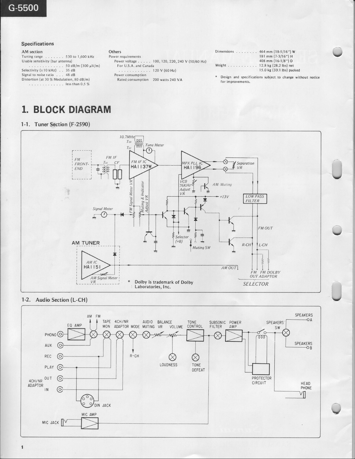
BLOCK
Tuner Section
530 to
(bar
antenna)
48
. . .
iill;f.'"xli?
Tif
DIAGRAM
(F
'l
dB
-2590l'
,600
(300
kHz
pvlm)
Others
Power reouirements
Power voltage
For U.S.A.
Power consumotion
Rated.consumption 200
10.7MHz
Tot
Toz
and Canada
m
I 00, 1
120
. .
Tune Meter
20, 220
(60
V
watts
,24O
Hz)
240 VA
V
(50/60
Hz)
Dimensions
Weight
.
+
Design
and specifications
for imorovements.
. . . 464
181
408
12.8
i
5.0 kg
(18-5/16")
mm
(7-3116"1H
mm
(16-1/8")D
mm
(28.2
kg
(311
subject
W
lbs) net
packed
lbs)
to change
\;
without notice
Audio
PHONO
AUX
REC
PLAY
OUT
4CHINR
ADAPTOR
IN
Section
EO AMP
@
@
@
e
@
Signal Meter
AM TUNER
T-----
(L-CH)
TAPE
4CHlNR
MON
ADAPTORMODE
a<
q)
t
\
-e<
o.\
.9
Fu
qI
!.:
-->
s
Aq
Lr_
Dolby
is trademark
i
Laboratories,
AUDIO
MUTTNG
-CH
R
76KHz4
Selector
(+a)
?A
uutino SW
I
of Dolby
Inc.
BALANCE TONE
VR VgTUME
LOUONESS
CONTROL
TONE
DEFEAT
AM
-V
Mutins
+
AM OUT
SUBSONIC POWER
FTLTER
AMp
FM
OUT
-_
SELECTOR
PROTECTOR
CIRCUIT
FM
OUT
L.CH
1
I
FM DOLBY
ADAPTOR
SPEAKERS"
U
MIC
JACK
MIC
AMP
DIN
JACK
o
Page 3
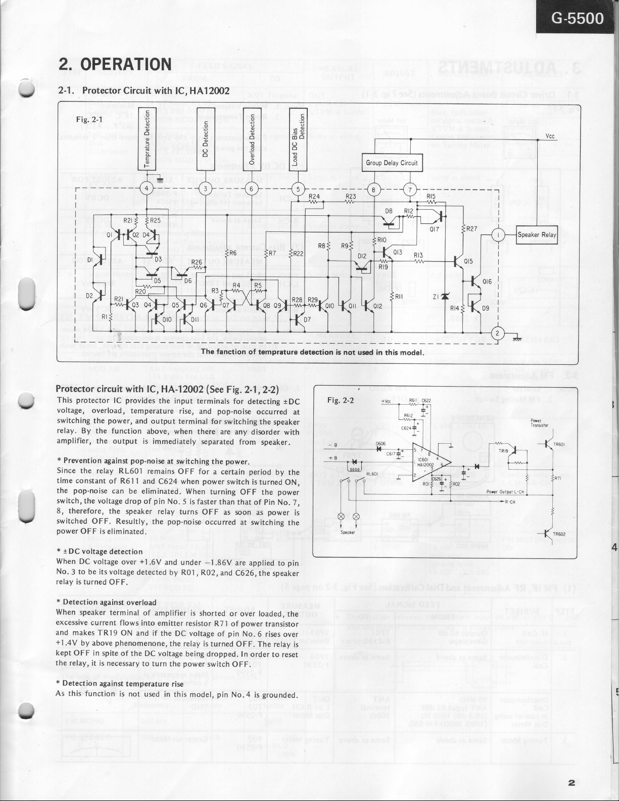
2.
OPERATION
2-1.
t/
Protector
Fis.2-1
Circuit
c
'F
I
o
o
o
o
f
N
E
o
F
with
lC, HA12W2
c
.;
o
o
o
o
o
o
o
O
c
.T
o
,^o
#E
o
o
o
J
'l
'\/
The
fanction
of temprature
detsction
is not
used in
this model.
v
J
Protector
This
voltage,
switching
relay.
amplifier,
*
Since
time
the
switch,
I
8, therefore,
switched
power
*
When
No.3
relay is turned
*
When
excessive
and
+1.4V
kept OFF
the
*
As
protector
overload,
the
By
the function
Prevention
the relay
constant
pop-noise
the
OFF.
OFF is
t
DC voltage
DC
voltage
to
be its voltage
Detection
speaker
current
makes
by
above
in spite
relay,
it is necessary
Detection
this
function
circuit
with lC, HA-12002
provides
lC
temperature
power,
and
the
output
against
of R61 1
can
voltage
the
eliminated.
detection
OFF.
against
terminal
TR19
against
is immediately
pop-noise
RL601
and
be eliminated.
drop of
speaker
Resultly,
+1.6V
over
detected
overload
of
flows
into
ON
and if
phenomenone,
of the DC
to turn
temperature
is
not
used in
the input
output
above,
at switching
remains
C624
pin
No.5
relay
pop-noise
the
and
by
amplifier
emitter
the
the
voltage
the
rise
(See
terminals
rise,
and
terminal
when there
OFF
turns
DC voltage
this
for
separated
the
for
power
when
When
turning
is
faster
OFF
occurred
-1.86V
under
R01,
R02,
is shorted
resistor
relay is
turned
being dropped.
power
switch
model,
Fig.2-'l,Z-2')
for
detecting
pop-noise
switching
are
any
disorder
from speaker.
power.
a certain
R71
of
pin
period
switch
OFF
than
that
as soon
at switching
are
applied
and
C626,the speaker
or
over loaded,
power
of
pin
No.6
OFF. The
In
orderto
OFF.
No.4
occu rred
the speaker
by
is turned
power
the
pin
of
No.
power
as
to
transistor
rises over
relay
grounded.
is
tDC
at
with
the
ON,
7,
is
the
pin
the
is
reset
./
t
Page 4
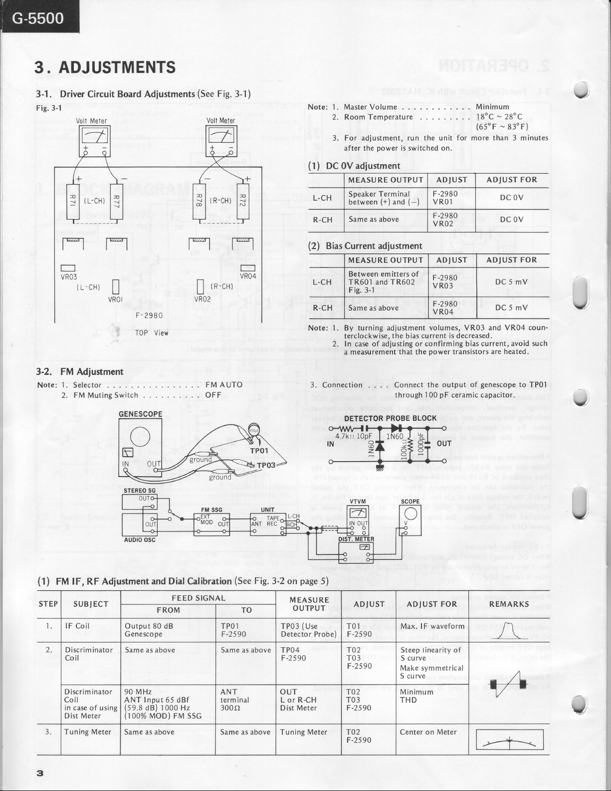
ADJUSTMENTS
3.
Driver
3-1.
Fig. 3-1
Circuit
Voll Meter
Board
Adjustments
(See
Volt N4eter
Fig.
3-1)
Note: 1. Master Volume
2. Room Temperature
3. For adjustment, run
after the
(1)
DC 0V adjustment
L.CH
R-CH
power
MEASURE
Speaker
between
Same as above
OUTPUT
Terminal
(+)and (-)
the unit for
is switched on.
ADf UST
-2980
F
VROl
F-2980
VRO2
Minimum
-
2g"c
1g"c
-
(os"F
more than 3 minutes
83"F)
ADf UST FOR
DC OV
DC
OV
Y'
FM Adjustment
3-2.
1
. Selector
Note:
2.
FM
Muting Switch
F-
2980
T0P View
GENESCOPE
STEREO SG
le
lg
AUDTO OSC
b
FM
OFF
FM
SSG
"hi8o
AUTO
off
TPOl
UNIT
o
qNT
o
TAPE^
"
REC
(2)
Bias Current
L-CH
R-CH Same as above
Note: 1.
3.
By turning adjustment
terclockwise,
2.
In case of
a measurement
Connection
DETECTOR
{ ol
T. METE
adjustment
MEASURE OUTPUT
Between em itters of
and TR602
TR601
Fig. 3-1
adjusting
VTVM
l4tl
tl
,
IN OUTI
a
o
o
F-2980
VRO3
F
VRO4
the
that the
Connect
through 1 00
PROBE BLOCK
volumes, VR03 and VR04
current
bias
confirming bias
or
power
the output
SCOPE
4
ADJ UST
-2980
is
decreased.
transistors
pF
ceramic
ADTUST FOR
DC5mV
DC5mV
current, avoid
are
heated.
genescope
of
capacitor.
to
coun-
such
TP01
J
'-a
v
(1)
FM lF, RF Adiustment
STEP
suBJ ECT
1. lF Coil
2.
Discrim
inato r
Coil
Discrim inator
Coil
in case of using
Dist Meter
3. Tuning Meter
(See
Dial
and
FROM TO
Output 80 dB
G enesco
90
ANT lnput 65 dBf
(s9.8
(100%
Same
pe
Same as above Same as above
MHz
dB) 1000 Hz
MoD)
as
above Same as above
Calibration
FEED
SIGNAL
FM SSG
TPOl
F-2590
ANT
term inal
300s-,
Fig.3-2
page
on
MEASURE
TPO3
Detector Probe)
TPO4
-2590
F
OUT
or
L
Dist Meter
Tuning
5)
OUTPUT
(Use
R-CH
Meter T02
ADf UST ADTUST FOR REMARKS
T01
-2s90
F
T02
T03
-2590
F
T02
T03
-2s90
F
F-2590
lF
Max.
waveform
Steep linearity of
rve
S cu
Make symmetrical
S curve
Minimum
THD
Center on Meter
\
v4r
FI
o
Page 5
'J
I
STEP
6.
(21
STEP
2.
ONEW
Input
urement
obtain
attenuater
however, the former
gether
The way of
suBJ ECT
4. 90
5.
MHz
Dial
Calibration
106
MHz
Dial
Calibration
MHz
90
RF
Adi.
MHz
106
RF Adi.
Signal Meter
Volume
FM STEREO
SUBJ ECT
1.
PLL
Adi.
vco
PLL
vco Adj.
of
ln case
using
Freq.
cou n te r.
Separation 98 MHz
Muting level
indicator
&
level
MEASUREMENT
signal
level
method
approximate
too.
under
is
indication of
modulation on
FROM
90 MHz
ANT Input 65
(59.8
dB) 1000
(100%
MoD) FM SSG
I06 MHz
ANT
Input
(s9.8
dB)
(100%
90 MHz
ANT
Value
1000
FM
106
ANT
Value with
1000
FM SSG
98 MHz
ANT
(59.8
(100%
Adjustment
98
ANT Input 65
(59.8
Pilot
SUBl
(100%
STEREO SG
98 MHz
ANT
(se.8
(no
ANT lnput 65 dBf
(s9.8
Pilot 19 kHz
R
Pilot
STE REO
98 MHz
ANT Input 18 dBf
(12.8
Pilot
SUBl kHz+Pilot
(100%
STE REO SG
1000 Hz
MoD)
Input Minimum
with sine wave
(100%
Hz
SSG
MHz
Input Minimum
(100%
Hz
Input 65 dBf
1000
dB)
MoD)
(See
MHz
dB)
FM
r 9 kHz
kHz+Pilot
MoD)
Input
dB)
FM
MOD)
dB)
Ffvl SSG
Mode 1
kHz
(100%
SG
dB)
FM
19
kHz
MoD)
FOR
provision
the
indicated
available
measurement,
by
power
general
FMSG
IHFM-T-200
FEED
SIGNAL
dBf
Hz
65 dBf
FM SSG
MOD)
sine
wave
MoD)
Hz
FM
SSG
Fig.
FEED SIGNAL
dBf
SSG
(9%
65 dBf
SSG
(9%
+
MOD)
SSG
(9%
3-2
MOD)
MOD)
MOD)
on
FM.
of
IHFM-T-200, a new
available power
"dBf",
ratio
(open
IHFM-T-i00
is
load
shown
abstract
below.
TO
Terminal
ANT
300s}
as above
Same
Same as above
as
Same
Same
,
ANT
3004
Same as above
Same as
Same
ratio
indication type);
is desisnated
page
terminal
as
above
as above
s)
above
above
meas-
"dBf"
from
0.8
To
to-
MEASURE
OUTPUT
OUT
or
R-CH
L
VTVM & Scope
as
Same
above
AD' UST
103
F-2s90
TCO3
F-2590
as above
Same
as above
Same
Signal
Meter
MEA5U
RE
OUTPUT
Stereo ind icator VRO5
TPO5
-2s90
F
Use Freq.
counter
OUT
L-CH
VTVM
&
Scope
Stereo ind
icator
o
The relation between the
FM
L0t,
F-2590
TCOl,
F-2590
VRO2
F-2s90
F-2590
VRO5
F
VRO4
F
VRO3
F
and the
former
SSG 65.8d8
ADI
-2590
-2s90
-2590
ADJ
Max.
on signal
VTVM &
Center
on
Tuning
L02
TCO2
Same
Same
J
3 on Meter
UST ADJ
Light
i 6 kHz
ouT
Muting
r8dBf(12.8
lnd icator
lighting level
18
dBf
standard
indication
"dB"
UST
FOR
Indication
meter-&
Scope.
Indication
Meter
as
above
as above
UST FOR
ind
icator
t200 Hz
-3s
dB
level
dB)
(1
2.8
dB)
input
is shown
REMARKS
rtt
88
I
Lllr'rl'r
I
-
l[;;l;-l
"
r,,'u"||,'r
/#
FI
REMA RKS
Adjust the VR05
within
center of
lighting
level
Confirm
L-CH
FM
ON
65 dBf
below.
separation
-+
R-CH
MUTING Switch
of
IHFM-T-200
ANT lnput
e2
lP
l,'rlr',1
59.8d8
:
t
-l
v
FM
MONO 1 000
FM
STEREO
modulation
frequency
Hz
1
000
Hz
modulation
mode
SUB
modulation
facto
100%
Pilot
+
Pilot
SUB
r
9%
100%
4
Page 6

3-3.
AM tF,
Note: 1.
STEP
l.
lF Coil Genescope
2.
600 kHz
Dial
Calibration
1400
Dial
Calibration
3. 600
RF Adi.
I
400 kHz
RF
4.
Signal Meter
volume
RF
Selector
2.
Confirm
SUBJ ECT
kHz
kHz
Adj.
Adjustment
point
start
FROM TO
45
(MoD
(MoD
kHz
(MoD
Input 60
(MOD
SSG
Input 54
(MoD
Hz
dB
60
Output
600 kHz
ANT !nput
400 Hz
AM SSG
1400 kHz
ANT lnput 60
400 Hz
AM SSG
600
ANT lnput 60 dB
400 Hz
AM sSG
1400 kHz
ANT
400 Hz
AM
1000 kHz
ANT
400
AM SSG
and
of
dial
FEED
dB
30%)
d B
30%)
30%)
dB
30%)
dB
30%)
Dial
Calibration
pointer
SIGNAL
TC04
F
AM
terminal
Same as
Same
Same as
Same
before
-2590
ANT
as above
as above
(See
AM
alignment.
VTVM
above
above
Fig.3-2
MEASU
OUTPUT
TPO6
-2590
F
REC
OUT
or
L
R-CH
VTVM
Same
Same as
Same
Signal Meter
Scope
&
as
above
above
as
above TC04
betow)
SCOPE
RE
AD,|
UST ADJ
CF04
-2s90
F
T04
-2s90
F
TCO5
-2590
F
L702
Bar
na
A nten
-2s90
F
VRO6
-2590
F
UST FOR
Max.
lF
waveform
Max.
Outpul
Same
as
as
Same
as above
Same
4 on
meter
J
REMARKS
1_L
above
I
above
Al^
JV
J
trl**:;-l
oAdiusting
FM&FM
o
VRO4
tr
S0l
r*t_-l
I
"o
5
or Connecting
Points on AM,
MPX circuit board,
0
TP04
T02
T
T03
T
o
Ll
o
V R02
I
n
VR05
a
TP05
109
o
o
/-\
TPo6
,\-,
VR06
F-2590
CFO3
E
o
TP03
F-2590
o
VR03
l-t
tl
T04
Ll0
o
CF02
E
| |
tl
108
o
|^|u"o'
Itcos@) | .)
Ircoz@ I
lrcoo@ |
L0/
lrr,,@ | O
| | Y
o
CFOI
fl
tl
ll
(r
\--l
)1
LOI
Fig.3-2
.
IP02
TOI
a
TPOI
oAbbreviations
Equipment
AM FM Generator
AM Standard
FM Standard Signal
FM Stereo Generator
Oscilloscope
Audio Oscillator
Others
Antenna
Modulation
Harmonic Distortion
Total
Oscilloscope
Signal Generator . . .
Generator . . .
.
Genescope
.
AM SSG
FM SSG
Stereo SG
.
Scope
.
Audio
.
. . ANT.
....MOD.
T.H.D.
Osc.
a
Page 7

OSince
4.
PARTS
I
4-1
-2865
. F
Conductor
LOGATION
Equalizer
Side
Circuit Board
PARTS
&
(Stock
No.
755141
LIST
)
Parts
Parts No. Stock No. Doscription
.Transistors
TR01,02 0300s00, 1
TR03,04 0300900,1
TR05,06 0306740,
TR07,08 0306740,
a
(-
c
c
c
R
R
R
F
R
R
R
R
some of
omitted from
Manual,
for
capacitors
pended previously
List
05,06 0620101
23,24
0625122
25,26 0620391
27,28
0625562
29,30 0620101
11 , 12 023'1 101
0231102
13.14
23,24 0200332
28 0200270
30 02ffi270
31,32 0231473
33,34 0231223
35,36 0231564
24 1
capacitors
parts
refer
0590
1
'l
lists
to the Common
&
resistors which
to each
254906 G,
254906 G,H 1C.A
2SC1845 E, F
2SC1845 E.
IOOpF
50V
1200pF
50V
39OpF
50V
560OpF 50V
IOOpF
50V
1/2W M.R. lC.A
100A
1kf,l 1/2W M.R. 1C.A
r
3.3k',
/2w
27A 1/2W
270 1/2W
47ka 1/2W M R. 1C.A
22kn 1/2W M.R. 1C.A
1/2W M.R. lC.A
560ka
4P Pin Ass'y Type D
and resistors
in this
Parts
Sansui Manudl.
H
F
P.C.
P.C
P.C.
P.C
P.C.
N.r.R.
N.r.R.
N.r.8.
are
Service
List
was ap-
lC,A
'rB.A
1B
1C.A
1C,A
1C.A
r C.A
2C.A
1C.A
v
4-2. F-2863 Tone Control Circuit
Conductor
4-3. F-2916
Conductor
Parts
Parts
oTra
TR601
TR602
TR603
VR601
J
Side
Mic
Side
List
No,
Stock No. Oescription
nsisto rs
0306070,1 2sci313 F,G
0300471 25A726(W) F,c
0306070 2SC1313 F
1OSO27O,1 20kO
601
243O4OO Mic Jack
Amp Circuit
Mic Mixing
{A)
Board
Volume
Board
(Stock
(Stock
No.7562741)
No.76't0421)
oConnector
Conectors
(3-'lOpins)
TypeA
NOTE:
Since stock number
shown in each
above parts
Pin
Ass'y
(3-10pins)
Type
A
(2-6pins)
Type
D
List
Parts
Parts No.
oTransistors
TR01.02
TR03.04 0306740
TR05.06
TR07,08
aVaristor
u
R
vR01,02 1015360
J 601 243O4OO Jack, headphone
Pin Ass'y
&
parts
list when
Type
Stock No. Description
0306740
0306070
0300470
03401 20
I
ut'uz
logaotso
37.38 0135221
TypeB(2-6pins)
|
of famale connectors
list
of Complete circurt
ordering the connector.
(3-1Opins
ype
B
E
{2-6pins)
2SC1B45 E, F
2SC1B45 E,
2SC1313
25A726
vD1212
MV.12
2204
5W Ce.R.
100k4
Treble
Bass &
(type
board,
Type
C
F
Type
F
F,
G
F,C
(C)
x 2,
Volume
Stock
2Pins 2420450
3Pins 2420460
3Pins(RED) 2420650
4Pins
2420470
242U8O
5Pins
242UgO
6Pins
B) with
wires are not
please
refer
(3-1Opins)
(2-6pins)
Position
1,24
1
1A
1,2C
1
1C
2B
No-
to the
,28
.2A
6
Page 8

4-4.
Conductor
-2980
F
Power
Side
Amplifier
Circuit
Board
(Stock
7572171
No.
)
List
Parts
No. Stock
Parts
o
nsistors
Tra
TR01.02
T803,04
T805,06
TR07,08
10 0306281,
TR09,
TA1^t
,12
TF13.14
TF15.16
TR17,18
TR19.20
TR 601
TR 602
TR 603
TB 604
olC
rc 601
.FET
FETO1
.Diodes
n ^1 n, I0311160
n ^< nA 10311160
D 601
602
D
603
D
D 604
D 605
606
D
.Zener
2D601
2D602
2D603
.ouoo
601
c
c 602
603
c
604
c
605
c
606
c
c 607
c 608
609
c
610
c
c 612
R
03,04
R
37,
,13,44
E
.9.
B
a
i1.i2
R
53.54
ir
59.60
r
65,66
" t1,72
a 17.78
R
81
r
601
R
602
q
604
R
605
B
606
B 61 6
R
61
01
L
HLbur
vR01,02
vR03,04
F 601
F 602
F 603
F 604
No. Description
0306740,
0306740,
0300721
0300721,
0306740,
0301090,
0308611.
0303441,
030]090.
!3C67,10.
0'$3232,
0308J92.
0308392.
0360900
1
037031
,02
180
r
031
'o31
1 1 80
0311700
0310350
0310350
0311290
1300
031
03i0350
Diodes
c3171
03i 71 80
031 71 80
70
uoui!!llll!
0655472
0655412
0655472
0655412
0655472
A655472
0655472
0655472
0655412
0655412
0549207
0212100
0200100
38
A200221
0200221
50
0200221
02A0221
02ao229
0200229
0153338
0153338
0212109
,82
02a1122
0212822
0201102
0185391
C185471
02A1102
a2a1102
7
4290310
,02
1 I
50400
i
lt tsoago
1034150
1034150
0432240
0432220
0432220
0432290
2310220
2310230
1
1
2
,
2
2
1
,
2SC1,845
2SC1845
D,
2SA85O
D,
2SA85O
2SC1735
2SC1B45
E, F
2SA992
D, E
2SD357
D,E
258527
E, F
2SA992
2SC1845
2SB5O7V1
2SD3134L
2SD3134L
'-
qi
2302
t.
25<12;
1
3t)
S247
1S1588
1524730
1 S1
588
R
B-1 52
(Red)
10D2
(Red)
1OD2
SS3
SS.3R
(Red)
10D2
(B)
RD
24F
(C)
BD,24F
(C)
RD.24F
(B)
RD.1BF
(C)
RD-1BF
4700pF 500V
50OV
4700pF
4700pF 500V
500V
4700pF
500V
4700pF
4700pF 500V
470OpF 500V
4700pF 500V
500V
4700pF
500V
4700pF
1000!F 63V
2W
1OO
10() 1/2W
1/2W
22OO
1/2W
220A
1/2W
220(]
1/2W
220s)
1/2W
2.2c,
1
2.2f,t
/2W
3W Ce.R.
0.33()
3W Ce.F.
0.334
N.l.R.
2W
1r)
lW
1.2Kfl
2W
8.2k0
'1kf2
lW
3900 5W
470rl 5W
1W
1ks)
1W N.l.B.
1kf,
RF Coil
lpH
Relay
Felay
B
10oo
B
1oo(]
2A25OV
25OV
144A
144A 25OV
125V
5A
Holder
Fuse
Holder
Fuse
F , F
E, F
E
E
E
D,
F
E,
E, F
'i
AL
F
E,
F
E,
\''
C.C.
C.C.
C.C.
E.C.
N.t.B.
N.t.R.
N.l.R.
N.l.R.
N.l.F.
N.l.R.
N.l.R.
N.l
N.l.R.
N.l.F.
N.l.R.
N.t.R.
I.R.
N
N.l.B.
Fure
AC
Fure
AC
Fuse
AC
AC Fuse
(L-arge)
(Small)
C.C.
C.C.
C.C.
C.C.
C.C.
C.C.
C.C.
R.
2C.2A
2C.24
2C,24
2C.24
?_3
7_C.24
2B
2C.2A
4A
?n
4A
4A
3B
2C.24
2C 2A
2C,2A
,._
'1(l
3C
3B
3B
3B
4A
3A
2B
4C
4C
/a
4C
4C
AA
AA
AA
4C
AA
1A.1A
2C2A
282A
2A
1C.1,A
1
B
1C'lA
1 B
1C
13
lC.]A
48
3C
48
4A,I
48
28
2A
1C 14
2B.2A,B
2c2A
4C
4C
4C
3C
I
J
1A
:
Carbon
: Solid
:
Cement
Metal
:
Resistor
Fusing
:
Resistor
Resistor
Resistor
Film
Resistor
N.l.R.
E.C.
BP.E.C.
Abbreviations
: Non-lnflammable
Resistor
CaPacitor
:
Mylar
: ElectrolYtic
Bi-Polar
:
Capacitor
CaPacitor
ElectrolYtic
O.C.
:
Ceramic
Capacitor
: Mica Capacitor
: Oil
Capacitor
:
Polystyrene
: Tantalum
Capacitor
Capacitor
Page 9

4-5. F-2590
Conductor
Side
Tuner
Circuit
Board
(Stock
No.
7522111)
3
4-t
4-'
44
4-t
4-
Co
v
I
v
v
Parts
List
Parts
No.
oTransistors
TB01
TR02
TF03
TR04
ranq
ram
rR07
rR08
rR09
TQ r1 1 !
TR l3
o
tCs
rc
01 0360350 HA1 137W
tc
02
lc
03 0360800 LA1240
.F
ETs
F.rnr lo37O12O,1
No, DoscJiption
Stock
0305801.2
030580'l
03061 13 2SC738 D
0306112
[0305730
0305950,
J
0305952,3
(0306090,1
10305730
0305950,
J
0305952,3
I
losooogo.
[0305731
0305951
1
10306090, 1
[o3o5731,2
10305951,2
t0306090, 1
0300470 2sA726 F
.r0305641
,0306390
0305730,1
:OT5732.3 2SC71
io3osgso,
0305952.3
0306090, 1 2SC1312R F,
0360320
t0370131,2
2SC1047
2SC1047 B, C
,2
2SC738
-
25C71 1 D, E,
2
1 2SC945
2SC945
2SC1312R F,G
"
25C71 1
2
1 2SC945
2SC945
1 2sc1312R
2SC71 1 E, F
,2
2SC945 P,
,2
2SC1312R
25C711
2SC945 P,
2sc1312R F,
2SC735
2SC1 636-1
2SC71 r D, E
1 2sc945
2SC945 K, P
HA1
3SK41 K, L
3SK41 il)
196
Parts No.
.Diodes
B.C
C
F
F
O,
K, P
F
E,
D.
R
O,
K. P
F, G
O
F.
G
E,F
O
G
'1
F,G
F
o,
c
K,L
2A
2A
1A
1B
JL
1B
1B
,1
2A
3C
1B
1C
3B
B
D
04 0311160
n n^
D 06
n onl [
.
isto rs
Var
D 01 0340120
D 03 0340120
01 0669350
c
05 0659015
c
06
C
ot
C
09 0661220
C
1 1
C
12
C
1 3
c
14
C
1
5 0669210
c
45
C
44,49 0620101
C
50,51 0620561
c
67 0669400
C
68 0661 150
C
69 0620361
C
84 0661 150
C
85 0661
C
L
01
L
o2
L
03
L
o4
No.
Stock
.l0311160
i
031 1 180
031
031
r
031 1 180
0669504
0669350
0663355
0679012
0669210
0669210
0629005
42OO72O
4210340 RF
422O4OO
4290110 100rrH
1 160
1 160
150
D6cription
152473D
152473D
1 S1
588
152473D
152473D
1
51 588
vD1212
vD1212
15pF
2200pF
4pF
15pF
22pF
20oF
1.spF
Capacitor
10pF
10pF
10pF
360pF
100pF
560pF 50V
15pF
15pF
360pF
15pF
15pF 50V C.C.
Antenna Coil
Coil
OSC
50V C.C.
50V C.C.
50V C.C.
50V C.C.
C.C.
SOY
C.C.
50V
500V Gimmick
5OV C.C.
50V C.C.
SOV
C.C.
P.C.
50V
P.C.
50V
P.C.
50V C.C.
50V C.C.
P.C.
50V
50V C.C.
Coil
Choke
Coil
2A
2B
2B
2A
2B
?n
2A
2A
3A
2A
2A
2A
2A
2A
2A
2C
1C
1C
2B
2B
2B
3B
3B
3A
2A
2A
2A
Parts
No.
Stck No.
L07
L08
L 10
T01
T02
T03
T04
T05
T06
cF 01 0910380
cF 02 0910380
cF 03 0910380
cF 04
L F 01 0910220
vR02
vB03 1035190
vR04
\/RnR I
v806
s
vc01
TC
49001
4900100
49001 10
4235930
14235990
423599 1
I
4236000
I
| 4236001
4220650
4290300
429001 1
091 0370
1035170
1035210
1034250
'
r
03425 1
10351 10
01 1110270
1220250
03 1
230090
Desc
00
3.3pH lnductor
3.3pH Inductor
100;rH Inductor
FM lF
FM
FM
FM
FM
AM
18pH Inductor
351rH Peaking
Ceramic
Ceramic
Ceramic F ilter
Ceram ic F ilter
Low Pass Filler
47ko
FM
100kO
Muting
220kf,2
1lf!1:1Y99
4.7kA
4.7ka
AM Signal Meter
De emphasis
A,M'FM
Trimmer
pt
ri
i on
Coil
lF Coil
lF
Coil
lF
Coil
lF
Coil
OSC Coil
Filter
Filter
(B)
Signai
1B)
Lever VR
{B)
(B)
(B)
Variab
Capacitcr
Coil
Coil
Meter V F
FM
Stereo
Separaiion VB
v!
V.C.O. vF
VR
Switch
e Caf:acitor
and
Position
3B
2B
3B
1A
2B
2B
2B
IA
1A
1B
2B
28
28
1 C
zc
38
1C
24
2A
4-'
Co
4-'
Page 10

46.
F-2862 Power
Parts
List
Parts No.
LD
601 0319050 LED
4-7.
48.
4-9.
-2862
F
Parts
List
Parts No.
LD601
F2878
Parts
List
Parts
No.
VROl
F-2879
Parts List
Parts No.
VROl
4-10. F2866
Conductor
Side
The circuit boards,
supplied as the
Indicator
Stock No. Dffiiption
(Green)
FM
Stereo
lndicator
No.
Stock
0319060 LED
Balance
Stock No.
1015320.
Volume
Stock
1011160,
Doscription
(Red)
Volume
D€scription
I 250k4
Circuit
No. Dtrription
1
1bOkO
(M,
(Bl
Tape Monitor/FM
F-2862,
assembled,
Circuit
power
Circuit Board
FM
srereo
Circuit
N)x
2
Balance Votume
Board
x 2 Volume
Muting
Mode
F-2878, F-2879, F-2866,
the individual
Board
Board
&
Switch
Circuit Board
parts
on
the circuit
F-2864,F-2868,F-2981,F-2867
boards, however,
4-13.
F-2981Power
are
&
provided
Transistor
Parts List
Parts
4-'14.
No.
.Transistors
TR601 0306780.1
TR602 0301 1 30, 1
oDiode
D 601 0340161.2
F-2981 Power
Conductor
Parts
List
Psrts
No. Stock No. De$ription
.Transistors
TR 601
TR602
.Varistor
D 601 0340161
No.
Stmk
De$ription
2SC2578LB O,
2SA1 1O3LB
STV-3H G,
Transistor
Side
SANSUI
F--P,.PS_T_?;
G)
1 2SA1
STV-3H G.
.2
'103L8
130,
0301
0306780,1 2SC2578LB
F-2854
are not
for orders.
Circuit Board
Y
Y
O,
Y
Circuit Board
O,Y
O,Y
(L-CH)
(R-cH)
Parts
Parts
.Oiode
u
our
S
01 1 1
S
02 1 131590 FM
4-'11.
F-2864Input
Conductor
Parts
Parts
List
No.
Stock No. Descriplion
r0311r60
logittgo
31560, 1 Tape Monitor
2410590
Side
List
No.
Stock No.
2090030
22@494 12P
152473D
1s158g
Muring & Mode
4P Pin Ass'v Type
Terminal
D€$ription
5P Din Socker
Input
Terminal
SW
SW
D
Circuit
Board
4-"15.
4-16.
F-2867
Conductor
Parts
Parts
s01 1 131570,
F-2854
Conductor
Tone
Side
List
No.
Stock No Dasc ripti
Audio Muting
Side
& Subsonic
on
I Tone
& Subsonic Filter
&
Loudness
Filter
Switch
SW
Switch
Circuit Board
Circuit Board
4-12.
F-2868
Parts List
Parts No.
s01 1
Speakers
No.
Stak
'13158C
'
Selector
Deription
Soo:<er Selector
Circuit
SW
Board
Parts
Parts
c 01
s0i
No.
,o2
List
Stock
No. Desription
0620511
1131560,1
51OpF sOV
Audi0Muting&
P.C.
LoudnessSW
a
Page 11

5.
OTHER
PARTS
5-1. Front
Parts
List
Parts
No. Stock
5727160
5456580
7008080
f5408311
15048121
15517270 MaskingPacking
4
5408580
5326690
5
131
1
24304C0
6
5058861 Bottom
7
5319081
I
1015360,'1 100ko
5319081
I
1015360, 1
View
No.
Description Parts
Wood
Bonnet
Inside
Panel
Front
Panel Ass'y
Front
Glass
Masking Plate
Dial Scale
Power Switch Knob
Power
650
Switch
Head
Phone Jack
Socket
Plate
Volume Knob
Bass
(C)
x
Treble Volume Knob
100kCl
2 Bass Volume
(C)
x 2 Treble Volume
No. Stck No.
10
5319181 Volume
1011160,1
1t
53191 33
101
11
IJ
14
t3
lo
17
5320, 1 25Ok0
5319172
5319142 Selector
1103600. I
551 6821 Les
5319133
1090270. 1
24T4N Microphone
53266S0
1 13156C,
Description Parts
Knob
150kO
x2Volume
{B)
Balance Volume Knob
(M.
N) x 2 Balance Volume
Tuning Knob
Selector Switcn
Mic
20kfl
Tape
1
Tape Monitor
Knob
Switch
Mixing Level Volume Knob
Mlc Mixing
iA)
Monitor
Jack
Switch
Switch
Socket
Knob
Level
Volume
No.
Stock No. Desc r iption
18
03 1 9060
19
5326690
1 13i590, 1
20
4301240
21
7116090
22
5326690
1 131560,1
z3
4301230,
24
5JZOOVU
1 1 3'1
25
5326690
1131580,1
26
031
,1
1
571
9050
FM
Stereo LED
FM Muting
FM
Muting & Mode
Tuning
Dial Pointer
Audio Muting
Audio Muting
Signal Meter
Tone
Tone
Speaker Selector Knob
Speaker Selector
Power
(Bed)
Mode
&
Meter
& LoudnessSwitch Knob
& Loudness
& Subsonic Filter
& Subrnic Filter
Switch
(Gren)
LED
Switch Knob
Switch
Switch
Switch
Switct,
Knob
U
5-2.
Top
STV3H
D601
STV3H
D601
T701-
!i?l-:--;
5702-------'--'
i-l
---i
; ;L-J
)__J
/
PL701
View
;-L-CH--1
TR6O1
2SC257B
r-
3--r_-
r
@ I i
i I
[t-
;i
7---LJ-------J
1__-'
F-2862
_--
-_i
ir-zaez;
i
r
;-R-CH1
\-/
F-29aO
i------l
,F-2854tr
lrl
'---|_-,
I
I
PL702
/,-L702
@<s
7/'re
+l
'
\ L-J
F-2590
r-zeee
i
I
L------{--4.--J
\---J
F-2462
r"l
i r /z-\
i-\!,
i
R702
Parts
List
Parts No.
1 2450070
2 2410091
3 2410830
4
5
/lll
6
7
I
9
oTransistors
TR 601 ( L-CH
TR601(R,CH)0301130,1
T8602(L-CH) 0301 130. 1
TR602(R,CH)
.
Diode
D 601
c 701
702
c
c 704
c 705
R
702
L 701
702
L
r
701
702
s
702
PL 701
Stck No, Description
AC
Outlet
6P Voltage Selector Plug
10P
Voltage Selector
6146670
7136083
2210310
52a64BO
3910490
5286450
0306780,
)
0306780,1
0340161,2
0605337
0659802
0559384
0559384
0103122 1.2ka 1/2W
4290021
4200830, 1
4002930
1131650
0400650
Pu lley
Tension U nit
Antenna Terminal
Bar Antenna Holder
Relie{
Strain
Bar Antenna
1
2SC2578LB
2SA1 103LB
2SA1.]03LB
2SC2578LB
STV-3H G,Y
O.033rrF 25OV M.C.
0.0047!F 150V
10000!F 50V
10000!F 50V
Balun
Bar Antenna
PowerTransformer
Power
Switch
8V 0.3A Pilot
(Antenna
Holder
Y
O,
Y
O,
O,Y
Y
O,
C.C
E.C.
E.C.
C.B.
Lamp
Board
{B)
Socket
Cord
)
9
Page 12

5-3.
Bottom
View
Parts List
ParG
No.
1
2
3
4
5 2200490
6 2230150
7 2090030
c
703
c 706
s 701
Stock
No.
7036620
3910600
3800470
22pO190
0602108
0602108
1 103600,1
Oescription
Tuning
Unit
Cord
Din
Terminal
Socket
1OOV
10OV
Switch
(AC
Strain Relief
AC
Speaker Terminal
1 2P Input
Ground,Terminal
5P
0.1pF
O.'lpF
Selector
M.C.
M.C.
Cord)
Board
6.
THREADING
lf a dial
cord is
unit
usei
of
cut
0.5
dial
As
The
this
length
Fis.6-2
FM
A M
Start-Point
1.
Threading of Dial
Thread
the
.
Cf ose
the variable
Stock
6036051
6146670
88190
J[30 600
dial cord
in numerical
No. Description
DIAL
OF
off
or slips,
replace
v
rlr
please
lw
Irl
800
mm0cord,
cord is approximately
,100
Cord
order
Cord
Pulley
from
(0.5
capacitor
Dial
Dial
completely.
CORD
it by foilowing
replace
it with
(66.9
170
cm
1 to 11
as Fig.
mm@)
procedures.
the sarne
type
inch).
6-1.
certainly.
2.
Attachment
1.
Set the dial
a
confirm
turning
that
the
of
pointer
to the start-point
the
dial
tuning
shaft.
Dial Pointer
pointer
runs smoothly
asFig.6-2.
on
the
dial scale
I
by
Page 13
7.
SCHEMATIC DIAGRAM
Audio & Power
Supply Section
V
lF:2866f-_-
rur-o-li-a
R37 2.2K
c4 /2mP c215600P
l$
ts
ta
l$
lsq
lrapt
uoor
r$
v
t_-1
v
-
F
v
(csA)
2862
[F-zie-f
t---
77
F66a5A
7?5V
2SD3I:
LRs
F-286:
p-Ho
lxEao
r/
ac t2
I
l_-9_
SPEAKERS
at#.+.*S$
r=f*
:
PHONE:
$d#fi
Page 14

*
Design
*
pr6sention
,La
*
Anderungen,
and specifications
et les
sp6cifications
die
dem
technischen Fortschritt
subject
to change
without notice for rmprovemenr.
sont
susceptibles
dienen,
d'Cter
bleiben
modifi6es
vorbehatten.
sans
pr6avls
par
suites d'am6liorations
6ventuelles
tF-2866T-_l
uor.rl
Irape
MoDE I
2-s-5ZTl
Fp-
uruFrr.rc
lruoro
I L.UDNESt
I
rR
IN
l+
Son
I
u\
xa
(d
p
I
il
,rl I
=
;ier
li
_:l
(,
solb
a<o
F 2b7e
MASTER
t__
fficE||j6ai6"-',rn
ry
sv
SR
ui,:mro,
Ctr0.002?
R,
JgK
-
R21
*o,f*c:r,=
T
TRoz
2SA992
2SC
1
845
.]t
W
25A726
2SA850
2SA906
2SC1313
2SC1
735
/' '/l
I,/l
Y)
t/
l'rli I
iltell
I
)
Pl |
'^
| S
zsar
ro:
25C2578
-:
).qtl
(aYl
lll
ffiil'
222
I tF
-
2867
",iJu,,
2SD357
to ll
ffl)
#r
[lUU
Bt'
HAl
2002
Rot
Rot
VR
IL
L
35
867
ftsr/.ZK
Rss
150
Deot
(Y,G)
TV-3H
TReaz
T.:T
Y"?,t'rt'
il|:i,
Ar .fl.'
h/T H+
u
l3?93"
'
lJ
srv.3H
A, DD
Hf \?
|l
RDrsF
RD24F
l|l
ul]
R
8152
Jl
rn =,)
TH TfT
llrlll
5b-J
<a\
ll'ffiflltfTt
*
\IU
U
SPEAKERS
PHONES
4645tr
EOTH CHAI,INIL
ffi*r,
-l
2-i'----
lF2eBTl
lzscz#e(o,nl
TReoz
Deot
TV-3H(Y,G)
Page 15

'Design
and specifications
'
pr6sention
La
*
Anderungen, die dem technischen Fortschritt dienen,
-2.
7
Tuner Section
.-l$'
i=:$:::$\=J\$SEiii
s^;
\68
rL n\
p=.:St=jSy=,iP=it
sBF=-:\FXsRFilqes
c
pS
s* F
:=iS"=Il"-I$':;R
EHHos:Hi:itSsrr
5Es
I
it$ $i$
tF$
subject to change
et les sp6cifications sont susceptibles d'eter modifi6es
;$r=So"*.,-fi
*
y"
-3
sH
!s"
S
6
6
"*-E.i
x,\
\!
Lx
$si
qiu
s$[
$
i$
rn
-osi
!s'
"
i$t
s
e
fr
ii
a;
without notice
|
|
i
ls ; i$
s
il
I
for improvement.
vorbehalten.
bleiben
-E
*
---ft-:s-r
'**-
=
*i,,-
$-.J-
(t
m ^ ^^,_-J
I
z
li{
N)N)
N
\
(,(r(r3
c) a) c)a
Scl
fu
ot
sans
-d i
pr6avis par
suites d'am6liorations 6ventuelles
r
l
"ffi'
fiffi
Litu9
t-o
a
"ffi'
ffi
UqiE
tLo
lly??
2SC738
s:
s
S)
25C131?
flr
6m
uuul
8u'
'ri
ffi
'lxill'
{f3'
ffi
N
a
tu!
Tll
N
(rx
(,
I
o,9
{-
3r
-l
'l
Iuu
HA1137W
HA1196
LA 1
240
rQ-r----
Wffitrtrlr'li
\o
ri
lsl58e
I
r- z_eE6
I
| ;'ti
IBiF
s
lsl
L-
M$!
(,
(rx
c) c)-n
,:l 6:
ES
*0
s
o"
ro9
6
,t"
J
p
,z*-(
/00Kr
tsz473D
N):
(r>d
\
1\)
o
-n
50v
I
Nr
(,];
c)x
!
(,
@
a)
NO
N-}l
G
-\l
\l
0.47t50V
Caz
Cat
/6V
N';t
+6
>R
=
(o
o,
yB*22611
R556.8K
z.
o
R5756K
ES
oq
-.1
ru
a
G
tr
N)
a
c)
(o
A
(t
<l
-ot
xl
i'i.,
()t
Tl
I 3t;93"
t|
nl
!Y
T'
Page 16

PACKING LIST 9.
8.
ACGESSORY PARTS LIST
Parts
No. Stock
1
2
3
A
6
MEMO
No. Description
16790
91
gO28141
9028151
9001420 Carton
5996080 Curl
Vinyl
Styiofoam
Styrofoam Packing
Stopper
Cover
Case
Packing
(Upper)
(Lower)
Stock No. Description
9204410
g237gz}
3820100
Operatinq I
Schematic Diaoram
FM Antenna
nstructions
sM112
Printed
Japan
in
(OBB230M)
 Loading...