

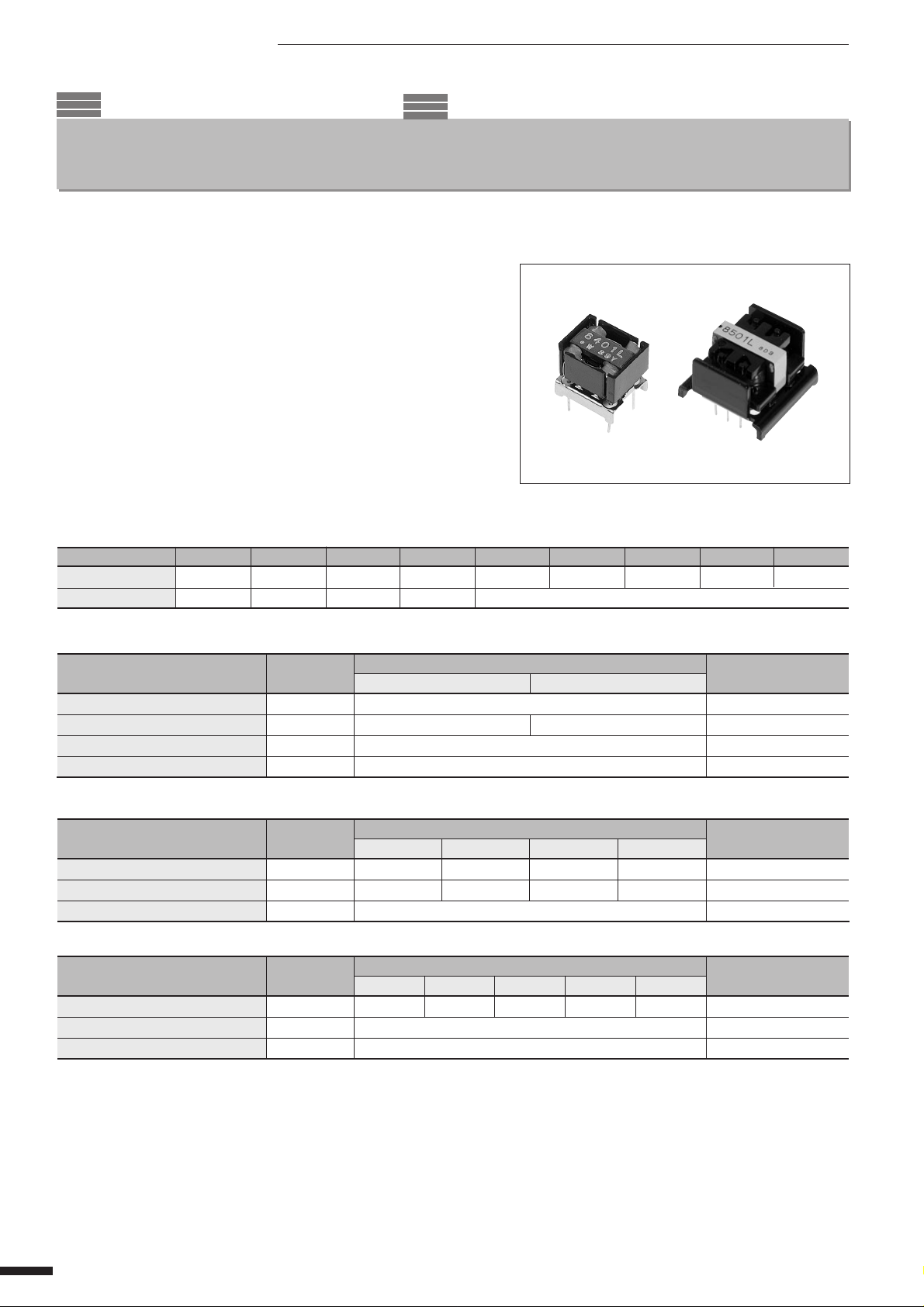
●SI-8400L/8500L Series
SI-8400L/8500L Series
Separate Excitation Switching Type with Coil
■Features
• Integrated switching IC and coil construction
• Requires 2 external components only
• Low switching noise
• Heatsink not required
• Built-in overcurrent and thermal protection circuits
• Built-in soft start circuit (Output ON/OFF control)...SI-8500L Series
■Applications
• Telephone power supplies
• Onboard local power supplies
■Lineup
Part Number SI-8401L SI-8402L SI-8403L SI-8405L SI-8501L SI-8502L SI-8503L SI-8504L SI-8505L
VO(V) 5.0 12.0 3.3 15.0 5.0 12.0 3.3 9.0 15.0
IO(A) 0.5 0.4 0.5 0.4 1.0
■Absolute Maximum Ratings
Parameter
DC Input Voltage
Power Dissipation
Junction Temperature
Storage T emperature
Symbol
VIN
PD
Tj
Tstg
SI-8400L SI-8500L
1.25 3
Ratings
35
+100
–25 to +85
Unit
V
W
°C
°C
■Recommended Operating Conditions
Parameter
DC Input Voltage Range
Output Current Range
Operating Temperature Range
Parameter
DC Input Voltage Range
Output Current Range
Operating Temperature Range
Symbol
VIN
IO
Top
Symbol
VIN
IO
Top
Ratings
SI-8401L SI-8402L SI-8403L SI-8405L
7 to 33 15 to 33 5.3 to 33 18 to 33
0 to 0.5 0 to 0.4 0 to 0.5 0 to 0.4
–20 to +85
Ratings
SI-8501L SI-8502L SI-8503L SI-8504L SI-8505L
7 to 33 15 to 33 5.3 to 33 12 to 33 18 to 33
0 to 1.0
–20 to +85
Unit
V
A
°C
Unit
V
A
°C
96
●SI-8400L/8500L Series
■Electrical Characteristics
Parameter
Output Voltage
Efficiency
Switching Frequency
Line Regulation
Load Regulation
Temperature Coefficient of Output Voltage
Switching Ripple
Voltage (C2=470µF)
Overcurrent Protection
Starting Current
Parameter
Output Voltage
Efficiency
Switching Frequency
Line Regulation
Load Regulation
Temperature Coefficient of Output Voltage
Switching Ripple
Voltage (C2=470µF)
Overcurrent Protection
Starting Current
Symbol
Conditions
Conditions
Conditions
∆VOLINE
Conditions
∆VOLOAD
Conditions
∆VO/∆Ta
∆Vr
Conditions
Conditions
Symbol
Conditions
Conditions
Conditions
∆VOLINE
Conditions
∆VOLOAD
Conditions
∆VO/∆Ta
∆Vr
Conditions
Conditions
VO
η
f
IS1
VO
η
f
IS1
Ratings
SI-8401L SI-8402L SI-8403L SI-8405L
min. typ. max. min. typ. max. min. typ. max. min. typ. max.
4.80 5.00 5.20 11.40 12.00 12.60 3.17 3.30 3.43 14.25 15.00 15.75
VIN=20V, IO=0.3A VIN=24V, IO=0.3A VIN=15V, IO=0.3A VIN=27V, IO=0.3A
80 88 75 89
VIN=20V, IO=0.3A VIN=24V, IO=0.3A VIN=15V, IO=0.3A VIN=27V, IO=0.3A
60 60 60 60
VIN=20V, IO=0.3A VIN=24V, IO=0.3A VIN=15V, IO=0.3A VIN=27V, IO=0.3A
80 100 100 130 60 80 100 130
VIN=10 to 30V, IO=0.3A VIN=18 to 30V, IO=0.3A VIN=8 to 30V, IO=0.3A VIN=21 to 30V, IO=0.3A
30 40 70 95 20 30 90 120
VIN=20V, IO=0.1 to 0.4A VIN=24V, IO=0.1 to 0.4A VIN=15V, IO=0.1 to 0.4A VIN=27V, IO=0.1 to 0.4A
±0.5 ±1.5 ±0.5 ±1.5
20 40 35 70 15 30 40 80
VIN=20V, IO=0.3A VIN=24V, IO=0.3A VIN=15V, IO=0.3A VIN=27V, IO=0.3A
0.55 0.45 0.55 0.45
VIN=10V VIN=18V VIN=8V VIN=21V
Ratings
SI-8501L SI-8502L SI-8503L SI-8504L SI-8505L
min. typ. max. min. typ. max. min. typ. max. min. typ. max. min. typ. max.
4.80 5.00 5.20 11.40 12.00 12.60 3.17 3.30 3.43 8.55 9.00 9.45 14.25 15.00 15.75
VIN=20V, IO=0.5A VIN=24V, IO=0.5A VIN=15V, IO=0.5A VIN=21V, IO=0.5A VIN=25V, IO=0.5A
83 89 79 87 90
VIN=20V, IO=0.5A VIN=24V, IO=0.5A VIN=15V, IO=0.5A VIN=21V, IO=0.5A VIN=25V, IO=0.5A
60 60 60 60 60
VIN=20V, IO=0.5A VIN=24V, IO=0.5A VIN=15V, IO=0.5A VIN=21V, IO=0.5A VIN=25V, IO=0.5A
70 130 70 130 50 80 70 130 70 130
VIN=10 to 30V, IO=0.5A VIN=18 to 30V, IO=0.5A VIN=8 to 30V, IO=0.5A VIN=15 to 30V, IO=0.5A VIN=21 to 30V, IO=0.5A
30 55 30 55 20 45 30 55 30 55
VIN=20V, IO=0.2 to 0.8A VIN=24V, IO=0.2 to 0.8A VIN=15V, IO=0.2 to 0.8A VIN=21V, IO=0.2 to 0.8A
±0.5 ±1.5 ±0.5 ±1.0 ±1.5
45 30 15 25 30
VIN=20V, IO=0.5A VIN=24V, IO=0.5A VIN=15V, IO=0.5A VIN=21V, IO=0.5A VIN=25V, IO=0.5A
1.1 1.1 1.1 1.1 1.1
VIN=18V VIN=24V VIN=12V VIN=21V VIN=25V
VIN=25V, IO=0.2 to 0.8A
(Ta=25°C)
Unit
V
%
kHZ
mV
mV
mV/°C
mVp-p
A
(Ta=25°C)
Unit
V
%
kHZ
mV
mV
mV/°C
mVp-p
A
97

●SI-8400L/8500L Series
■Outline Drawing
IN
rV
a
b
14.5
±0.5
q
Vo
Terminal 1 marking
φ
0.8max.
(10.16) (7.62) (2.19)(2.17)
■Block Diagram
SI-8400L SI-8500L
V
IN
IN
L
y
r
e
L
IN
±0.5
12
GND
w
±0.6
13.2
±0.2
10
±0.6
4.7
a. Part Number
b. Lot Number
Open Air Type
Weight: Approx. 5.1g
a
b
SK
qwe
V
OUT
SS GND
±0.1
26
Terminal 1 marking
0.6
φ
418
±0.1
18
3.7
(unit:mm)
a. Part Number
b. Lot Number
26
Open Air Type
Weight: Approx. 14.5g
2
SI-8400L SI-8500L
41
IN VO
V
MIC1
Reg. OCP
OSC Reset
Comp.
Amp.
■Standard External Circuit
3
LIN
L1
61
V
IN
MIC
1
4
L
IN
L
1
V
O
Reg. OCP
Latch
Drive
TSD
&
OSC Reset
Comp.
Di1
Latch
&
Drive
TSD
Di
1
Amp.
V
REF
2
GND
S.S.
V
REF
32
GND
V
GND
IN
++
C
1
220µF
IN
V
SI-8400L
2
Pin compatible with SI-8200L
98
V
OUT
14
LINGND
3
N.C
V
O
C
2
470µF
GND
V
V
GND
IN
++
C
1
470µF
IN
V
SI-8500L
2
C
3
OUT
LINGNDS.S
34
N.C
16
C3 is necessary only for using soft start function.
Pin compatible with SI-8300L
C
470µF
V
O
2
GND

■Ta-PD Characteristics
1.5
SI-8400L
3.0
SI-8500L
●SI-8400L/8500L Series
100
PD=VO•IO
ηχ
–1
(W)
D
1.0
0.5
Power Dissipation P
0
02550
Ambient Temperature Ta (°C)
75 100
(W)
D
2.0
1.0
Power Dissipation P
0
0 25 50 75 100
Ambient Temperature Ta (°C)
■SI-8500L application circuit
Terminal no.2 is for soft start. Connecting a capacitor to the terminal
enables the soft start function. See page 85 for the f ormulas to calculate delay time and rise time. Output can be turned on and off by
using the soft start terminal. To stop output, set the soft start terminal
voltage to VSSL (0.2V typ.) or less. To switch the potential of the soft
start terminal, drive the open collector of the transistor. Since the
discharge current from C3 flows to the ON/OFF control transistor , limit
the current for protection. The SS terminal is pulled up to the power
supply in the IC and no external voltage can be applied.
VO :Output voltage
IO :Output current
ηχ :Efficiency (%)
The efficiency depends on the input
voltage and the output current. Thus,
obtain the value from the efficiency
graph and substitute the percentage
in the formula above.
SI-8500L SI-8500L
S.S.2 S.S.2 S.S.
C
3
O.
ON/OFF Soft start Soft start +VO ON/OFF
V
SI-8500L
2
3
C
■Caution
1. Allocation of Components
For the best operating environment, the ground should be a single g round line at the GND terminal (terminal 2 on the SI-8400L, terminal 3 on
the SI-8500L), and the wiring from C1 and C2 to ground should be as short as possible.
2. Capacitors C1 and C2
1) They must satisfy the breakdown voltage and allowable ripple current.
Exceeding the ratings of these capacitors or using them without derating shortens their service lives and may also cause abnormal
oscillation of the IC.
2) C2 must be a low-impedance type capacitor to ensure minimum ripple voltage and stable switching operation.
3) C3 (SI-8500L only) is a capacitor for soft start. When not using soft start, leave terminal 2 open. It is pulled up inside the IC.
3. Terminals LIN and NC in the connection diagram must be left unconnected to other circuits.
4. The IC's metalic heatsink is electrically floating. Do not connect it to GND or any other circuit.
5. Since the SI-8400L and 8500L series have an open-package construction, they can only be operated in specific environments. Verify the
operating environment and use the conditions indicated in the reliability data.
99

●SI-8400L/8500L Series
■Typical Characteristics (SI-8400L Series)
Rise Characteristics(SI-8401L) Efficiency Characteristics(SI-8401L) Load Regulation(SI-8401L)
T
a
6
5
(V)
O
4
3
2
0.1A
=0A
O
I
0.5A
0.3A
=25°C
Output Voltage V
1
0
0
246
810
Input Voltage VIN (V)
Temperature Characteristics(SI-8401L)
100
90
80
70
60
50
40
Efficiency η (%) Frequency f (kHz)
00
–40
–20 0 20
Ambient Temperature Ta (°C)
VIN=20V, IO=0.3A
η
V
O
f
40 60 80 100
100
Efficiency η (%)
5.3
5.2
5.1
(V)
O
5.0
4.9
4.8
Output Voltage V
4.7
90
80
V
IN
7V
10V
70
20V
25V
60
33V
50
0
0
0.1 0.2 0.3 0.4 0.5
Output Current IO (A)
Overcurrent Protection Characteristics(SI-8401L) Thermal Protection Characteristics(SI-8401L)
6
5
(V)
O
4
3
2
Output Voltage V
1
0
0
20V
=7V
IN
V
33V
0.5 1.0 1.5 2.0
Output Current IO (A)
T
T
a
=25°C
a
=25°C
20V
25V
33V
10V
7V
5.3
5.2
(V)
5.1
O
5.0
4.9
Output Voltage V
4.8
0
0
0.1 0.2 0.3 0.4 0.5
6
5
(V)
4
O
3
2
Output Voltage V
1
0
0
50 100
Case Temperature TC (°C)
VIN=33V
10V
7V
Output Current IO (A)
20V
IN
=20V, IO=20mA
V
150 200
T
a
=25°C
Note on Thermal Protection:
The thermal protection circuit is intended for protection against heat during instantaneous shortcircuiting. Its operation is not guaranteed for shortcircuiting over extended periods of time.
Rise Characteristics(SI-8402L) Efficiency Characteristics(SI-8402L) Load Regulation(SI-8402L)
14
12
10
(V)
O
8
6
4
Output Voltage V
2
0
0
510
Input Voltage VIN (V)
0.2A
O
I
=0A
0.4A
T
a
=25°C
15 20
100
90
80
70
60
Efficiency η (%)
=15V
IN
V
24V
33V
50
0
0
0.1 0.2 0.3 0.4
Output Current IO (A)
Ta=25°C
12.3
12.2
(V)
12.1
O
12.0
11.9
Output Voltage V
11.8
0
0.1 0.2 0.3 0.4
0
V
IN
=33V
24V
20V
15V
Output Current IO (A)
Ta=25°C
100

■Typical Characteristics (SI-8500L Series)
●SI-8400L/8500L Series
Rise Characteristics(SI-8501L) Efficiency Characteristics(SI-8501L) Load Regulation(SI-8501L)
T
a
a=25°C
7
6
5
4
3
2
Output Voltage VO (V)
1
0
0.5A
=0A
O
1A
I
0
5101520
Input Voltage VIN (V)
T
Temperature Characteristics(SI-8401L)
V
IN
100
90
80
70
60
50
40
Efficiency η (%) Frequency f (kHz)
0
–40
0 40 80 120
Ambient Temperature Ta (°C)
=20V, IO=0.5A
η
V
O
f
100
Efficiency η (%)
5.15
5.10
5.05
(V)
O
5.00
4.95
4.90
Output Voltage V
4.85
0
90
=7V
IN
V
80
20V
33V
70
60
50
40
0
0.25 0.5 0.75 1
0
Output Current IO (A)
Overcurrent Protection Characteristics(SI-8401L) Thermal Protection Characteristics(SI-8401L)
7
6
5
(V)
O
4
3
2
Output Voltage V
1
0
0
1234
33V
=7V
20V
IN
V
Output Current IO (A)
=25°C
Ta=25°C
5.15
5.10
5.05
5.00
4.95
4.90
Output Voltage VO (V)
4.85
0
0
7
6
5
(V)
O
4
3
2
Output Voltage V
1
0
0
V
IN
=33V
20V
15V
7V
0.25 0.5 0.75 1
Output Current IO (A)
40 80 120 160
Ambient Temperature Ta (°C)
a=25°C
T
VIN=20V, IO=0A
Note on Thermal Protection:
The thermal protection circuit is intended for protection against heat during instantaneous shortcircuiting. Its operation is not guaranteed for shortcircuiting over extended periods of time.
Rise Characteristics(SI-8502L) Efficiency Characteristics(SI-8502L) Load Regulation(SI-8502L)
14
12
10
(V)
O
8
6
4
Output Voltage V
2
0
0
5101520
Input Voltage VIN (V)
0.5A
=0A
O
I
Ta=25°C
1A
100
Efficiency η (%)
90
=15V
IN
V
33V
80
24V
70
60
50
40
0
0.25 0.5 0.75 1.0
0
Output Current IO (A)
Ta=25°C
Output Voltage VO (V)
12.3
12.2
12.1
12.0
11.9
11.8
11.7
18V
15V
24V
VIN=33V
0
0.25 0.5 0.75 1
0
Output Current IO (A)
Ta=25°C
101
 Loading...