

SanKen STR-A6051M, STR-A6052M, STR-A6053M, STR-A6059H, STR-A6061H Schematic [ru]
...
VAC
C1
C
6
R
1
D
1
BR
1
R2
C2
T1
D
P
PC1
C3
R
OCP
C
Y
C5
1 2 3 4
D/ST D/STBRNC
S/OCP FB/OLP
GND
VCC
8 7
5
STR-A6000
U1
D2
C4
R
C
R
B
R
A
D51
C51
R51
R52
U51
R54
R56
C52
S
PC1
R53
R55
L51
C53
VOUT
(+)
TC_STR-A6000_1_R1
(-)
Products
P
(Adapter)
P
(Open frame)
AC230V
~265V
AC230V
~265V
f
OSC(AVG)
= 67 kHz
f
OSC(AVG)
= 100 kHz
Off-Line PWM Controllers with Integrated Power MOSFET
STR-A6000 Series Data Sheet
General Descriptions
The STR-A6000 series are power ICs for switching
power supplies, incorporating a MOSFET and a current
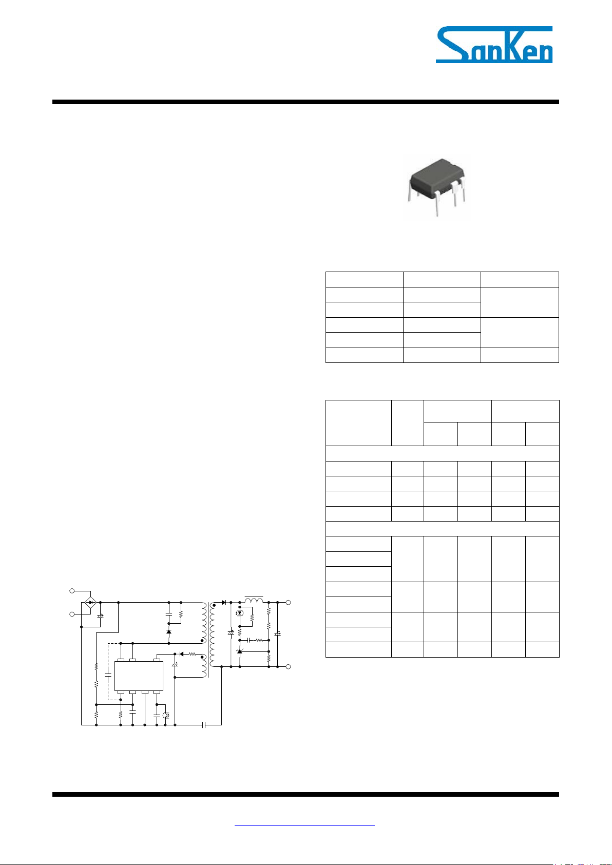
Package
DIP8
mode PWM controller IC.
The low standby power is accomplished by the
automatic switching between the PWM operation in
normal operation and the burst-oscillation under light
load conditions. The product achieves high
cost-performance power supply systems with few
external components.
Not to Scale
Lineup
Features
• Current Mode Type PWM Control
• Brown-In and Brown-Out function
• Auto Standby Function
No Load Power Consumption < 25mW
• Operation Mode
Normal Operation ----------------------------- PWM Mode
Standby ---------------------------- Burst Oscillation Mode
• Random Swit ching Functi on
• Slope Compensation Function
• Leading Edge Blanking Function
• Bias Assist Function
• Audible Noise Suppression function during Standby
mode
• Protections
・Overcurrent Protection (OCP)*; Pulse-by-Pulse,
built-in compensation circuit to minimize OCP point
variation on AC input vol tage
・Overload Protection (OLP); auto-restart
・Overvoltage Protection (OVP); latched shutdown
・Thermal Shutdown Protection (TSD); latched shutdown
*STR-A60××H D has two types OCP
Typical Application Circuit
• Electrical Characteristics
V
(min.) f
DSS
STR-A605×M 650 V
STR-A607×M 800 V
STR-A605×H 650 V
STR-A606×H 700 V
STR-A606×HD 700 V 100 kHz
*STR-A60××HD has two types OCP
• MOSFET ON Resistance and Output Power, P
OUT
R
Products
STR-A6051M 3.95 Ω 18.5 W 14 W 31 W 21 W
STR-A6052M 2.8 Ω 22 W 17.5W 35 W 24.5 W
STR-A6053M 1.9 Ω 26 W 21W 40 W 28 W
STR-A6079M 19.2 Ω 8 W 6 W 13 W 9 W
STR-A6059H
STR-A6069HD
STR-A6061H
STR-A6061HD
STR-A6062H
STR-A6062HD
STR-A6063HD 2.3 Ω 25 W 20 W 40 W 28 W
* The output power is actual continues power that is measured at
50 °C ambient. The peak output power can be 120 to 140 % of the
value stat ed here. Core size, ON Duty, and thermal design affect
the output power. It may be less than the value stated here.
DS(ON)
(max.)
AC85
6Ω 17 W 11 W 30 W 19.5 W STR-A6069H
3.95Ω 20.5 W 15 W 35 W 23.5 W
2.8 Ω 23 W 18 W 38 W 26.5 W
Applications
STR-A6000-DSJ Rev.4.4 SANKEN ELECTRIC CO., LTD. 1
Mar. 13, 2015 http://www.sanken-ele.co.jp/en
© SANKEN ELECTRIC CO., LTD. 2008
• Low power AC/DC adapter
• White goods
• Auxiliary power supply
• OA, AV and industrial equipment
OSC(AVG)
67 kHz
100 kHz
OUT
OUT
*
AC85

STR-A6000 Series
Contents
General Descriptions ------------------------------------------------------------------------------------------ 1
1. Absolute Maximum Ratings --------------------------------------------------------------------------- 3
2. Electrical Characteristics ------------------------------------------------------------------------------ 4
3. Performance Curves ------------------------------------------------------------------------------------ 6
3.1 Derating Curves ------------------------------------------------------------------------------- 6
3.2 Ambient Temperature versus Power Dissipation Curve ------------------------------ 6
3.3 MOSFET Safe Operating Area Curves --------------------------------------------------- 7
3.4 Transient Thermal Resistance Curves ---------------------------------------------------- 9
4. Functional Block Diagram --------------------------------------------------------------------------- 11
5. Pin Configuration De finitions ----------------------------------------------------------------------- 11
6. Typical Application Circuit -------------------------------------------------------------------------- 12
7. Package Outline ---------------------------------------------------------------------------------------- 13
8. Marking Diagram -------------------------------------------------------------------------------------- 13
9. Operational Description ------------------------------------------------------------------------------ 14
9.1 Startup Operation --------------------------------------------------------------------------- 14
9.2 Undervoltage Lockout (UVLO)----------------------------------------------------------- 15
9.3 Bias Assist Function ------------------------------------------------------------------------- 15
9.4 Constant Output Volt age Control -------------------------------------------------------- 15
9.5 Leading Edge Blanking Function -------------------------------------------------------- 16
9.6 Random Switching Function -------------------------------------------------------------- 16
9.7 Automatic Standby M ode Function ----------------------------------------------------- 16
9.8 Brown-In and Br own-Out Function ----------------------------------------------------- 17
9.8.1 DC Line Detection ------------------------------------------------------------------------ 17
9.8.2 AC Line Detection ------------------------------------------------------------------------ 18
9.9 Overcurrent Protection Function (OCP) ----------------------------------------------- 19
9.10 Overload Protection Function (OLP)---------------------------------------------------- 20
9.11 Overvoltage Protection (OVP) ------------------------------------------------------------ 20
9.12 Thermal Shutdown Function (TSD) ----------------------------------------------------- 20
10. Design Notes -------------------------------------------------------------------------------------------- 21
10.1 External Components----------------------------------------------------------------------- 21
10.2 PCB Trace Layout and Component Placement --------------------------------------- 22
11. Pattern Layout Example ----------------------------------------------------------------------------- 24
12. Reference Design of Power Supply ----------------------------------------------------------------- 25
Important Notes ---------------------------------------------------------------------------------------------- 27
STR-A6000-DSJ Rev.4.4 SANKEN ELECTRIC CO., LTD. 2
Mar. 13, 2015 http://www.sanken-ele.co.jp/en
© SANKEN ELECTRIC CO., LTD. 2008

STR-A6000 Series
A6059H / 69H
/ 69HD
A6051M / 61H
/ 61HD
A6052M / 62H
/ 62HD
A6059H / 69H
/ 69HD
MOSFET Power
Dissipation
Control Part Power
Dissipation
Operating Ambient
Temperature
1. Absolute Maximum Ratings
Current polarities are defined as follo ws: current going into the IC (sinking) is po sitive current (+) ; and current coming
out of the IC (sourcing) is negative current (−).
Unless otherwise specified, T
Parameter
= 25 °C, 7 pin = 8 pin.
A
Symbol Test Conditions Pins Rating Units Remarks
1.2
1.8
Drain Peak Current
(1)
I
Single pulse 8 – 1
DPEAK
2.5
A
3.0
4.0
I
Avalanche Energy
S/OCP Pin Voltage
(2)(3)
=1.2A
LPEAK
I
=1.8A
LPEAK
I
=2A
LPEAK
I
=2A
LPEAK
I
LPEAK
I
LPEAK
I
LPEAK
I
LPEAK
=2.2A
=2.3A
=2.5A
=2.7A
8 – 1
1 − 3 −2 to 6 V
V
EAS
S/OCP
7
24
46
47
56
62
72
86
mJ
BR Pin Voltage VBR 2 − 3 −0.3 to 7 V
BR Pin Sink Curr ent IBR 2 − 3 1.0 mA
A6079M
A6053M / 63HD
A6079M
A6061H / 61HD
A6051M
A6062H / 62HD
A6052M
A6063HD
A6053M
FB/OLP Pin Voltage
FB/OLP Pin S ink Current
VCC Pin Voltage
(4)
VFB 4 − 3 −0.3 to 14 V
IFB 4 − 3 1.0 mA
VCC 5 − 3 32 V
PD1
(5)
8 – 1 1.35 W
PD2 5 – 3 1.2 W
(6)
Storage Temperature T
TOP — −20 to 125 °C
— −40 to 125 °C
stg
Channel Temperature Tch — 150 °C
(1)
Refer to 3.3 MOSFET Safe Operating Area Curves
(2)
Refer to Figure 3-2 Aval anche Energy Derating Coe fficient Curve
(3)
Single pulse, V
(4)
Refer to Figure 3-3 Ambient temperature versus power dissipation curve
(5)
When embedding this hybrid IC onto the printed circuit board (cupper area in a 15 mm × 15 mm)
(6)
The recommended internal frame temperature, TF, is 115°C (max.)
= 99 V, L = 20 mH
DD
STR-A6000-DSJ Rev.4.4 SANKEN ELECTRIC CO., LTD. 3
Mar. 13, 2015 http://www.sanken-ele.co.jp/en
© SANKEN ELECTRIC CO., LTD. 2008
STR-A6000 Series
Test
Conditions
Startup Circuit Operation
Voltage
= 13.5 V
Startup Cur rent Biasin g
Threshold Voltage
I
OCP Threshold Voltage at
Zero ON Duty
OCP Threshold Voltage at
36% ON Duty
OCP Threshold Voltage in
Leading Edge Blanking Time
FB/OLP pin Oscillation Stop
Threshold Voltage
2. Electrical Characteristics
Current polarities are defined as follows: current going into the IC (sinking) is positive current (+); and current
coming out of the IC (sourcing) is negative current (−).
Unless otherwise specified, T
Parameter Symbol
= 25 °C, VCC = 18 V, 7 pin = 8 pin.
A
Pins Min. Typ. Max. Units Remarks
Power Supply Start up Operation
Operation Start Voltage V
Operation Stop Voltage
(1)
V
Circuit Current in Operation I
V
Startup Cur rent I
STARTUP
V
Normal Operation
Average Switching
Frequency
f
OSC(AVG)
Switching Frequency
Modulation Deviation
Maximum ON Duty D
Minimum O N Time t
ON(MIN)
Protection Function
CC(ON)
CC(OFF)
CC(ON)
ST(ON)
CC(BIAS)
V
V
= − 100 µA
CC
CC
CC
= 12 V
5 − 3 13.8 15.3 16.8 V
5 − 3 7.3 8.1 8.9 V
5 − 3 — — 2.5 mA
8 − 3 — 38 — V
5 − 3 − 3.7 − 2.5 − 1.5 mA
5 − 3 8.5 9.5 10.5 V
60 67 74
8 − 3
kHz
90 100 110
— 5 —
Δf 8 − 3
kHz
— 8 —
MAX
8 − 3 77 83 89 %
— 540 — ns
8 − 3
— 470 —
A60××M
A60××H / HD
A60××M
A60××H / HD
A60××M
A60××H / HD
Leading Edge Blanking Time tBW
OCP Compensation
Coefficient
OCP Compensation ON Duty
DPC
D
V
V
V
OCP(LEB)
Maximum Feedback Current I
Minimum Feedback Current I
FB(MAX)
FB(MIN)
V
OLP Threshold Voltage V
OLP Operation Current I
CC(OLP)
OLP Delay Time t
(1)
V
CC(BIAS)
> V
CC(OFF)
always.
—
— 280 —
— 20 —
— 340 —
—
— 33 —
DPC
OCP(L)
OCP(H)
V
= 32 V
CC
— — 36 — %
1 − 3 0.70 0.78 0.86 V
1 − 3 0.81 0.9 0.99 V
1 − 3 1.32 1.55 1.78 V
V
= 12 V
CC
V
= 12 V
CC
4 − 3 − 340 − 230 − 150 µA
4 − 3 − 30 − 15 − 7 µA
4 − 3 0.85 0.95 1.05 V
4 − 3 7.3 8.1 8.9 V
5 − 3 − 300 600 µA
— 54 68 82 ms
FB(STB)
FB(OLP)
OLP
A60××M
ns
A60××H / HD
A60××M
mV/μs
A60××H / HD
A60××HD
STR-A6000-DSJ Rev.4.4 SANKEN ELECTRIC CO., LTD. 4
Mar. 13, 2015 http://www.sanken-ele.co.jp/en
© SANKEN ELECTRIC CO., LTD. 2008
STR-A6000 Series
Test
Conditions
Brown-Out Threshold
Voltage
BR Function Disabling
Threshold
Latch Circuits Holding
Current
Thermal Sh ut down Operat ing
Temperature
A6059H / 69H
/ 69HD
A6051M / 61H
/ 61HD
A6052M / 62H
/ 62HD
Channel to Case Thermal
Resistance
Parameter Symbol
FB/OLP Pin Clamp Voltage V
FB(CLAMP)
Brown-In Threshold V oltage V
V
BR Pin Clamp Voltage V
BR(CLAMP)
V
OVP Threshold Voltage V
(2)
I
CC(LATCH)
MOSFET
Drain-to-Source Breakdown
Voltage
Drain Leakage Current I
Pins Min. Typ. Max. Units Remarks
4 − 3 11 12.8 14 V
V
BR(IN)
BR(OUT)
BR(DIS)
CC(OVP)
T
— 135 — — °C
j(TSD)
= 32 V
CC
V
= 32 V
CC
V
= 32 V
CC
V
= 32 V
CC
V
= 9.5 V
CC
2 − 3 5.2 5.6 6 V
2 − 3 4.45 4.8 5.15 V
2 − 3 6 6.4 7 V
2 − 3 0.3 0.48 0.7 V
5 − 3 26 29 32 V
5 − 3 — 700 — μA
650 — —
8 – 1
V
DSS
700 — —
800 — — A607×
8 – 1 — — 300 μA
DSS
— — 19.2
V
A605×
A606×
A6079M
— — 6
On Resistance
R
DS(ON)
I
= 0.4A
DS
8 − 1
— — 3.95
Ω
— — 2.8
A6063HD
A6053M
A6053M
Switching Time
Thermal Resistance
(3)
— — 2.3
— — 1.9
— — 250 ns
tf 8 – 1
— — 400 ns
θ
ch-C
— — — 22 °C/W
(2)
A latch circuit is a circuit operated with Overvoltage Protection function (OVP) and/or Thermal Shutdown function
(TSD) in operation.
(3)
θ
is thermal resistance between channel and case. Case temperature (TC) is measured at the center of the case top
ch-C
surface.
STR-A6000-DSJ Rev.4.4 SANKEN ELECTRIC CO., LTD. 5
Mar. 13, 2015 http://www.sanken-ele.co.jp/en
© SANKEN ELECTRIC CO., LTD. 2008
STR-A6000 Series
Safe Operating Area
Temperature Derating Coefficient (%)
1.35W
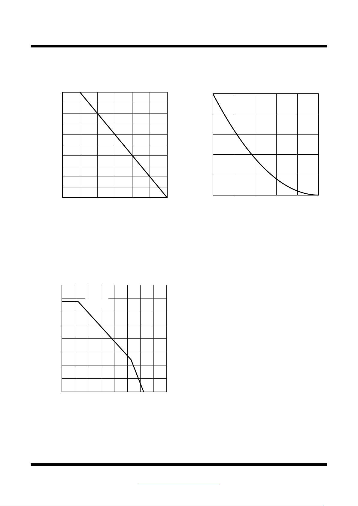
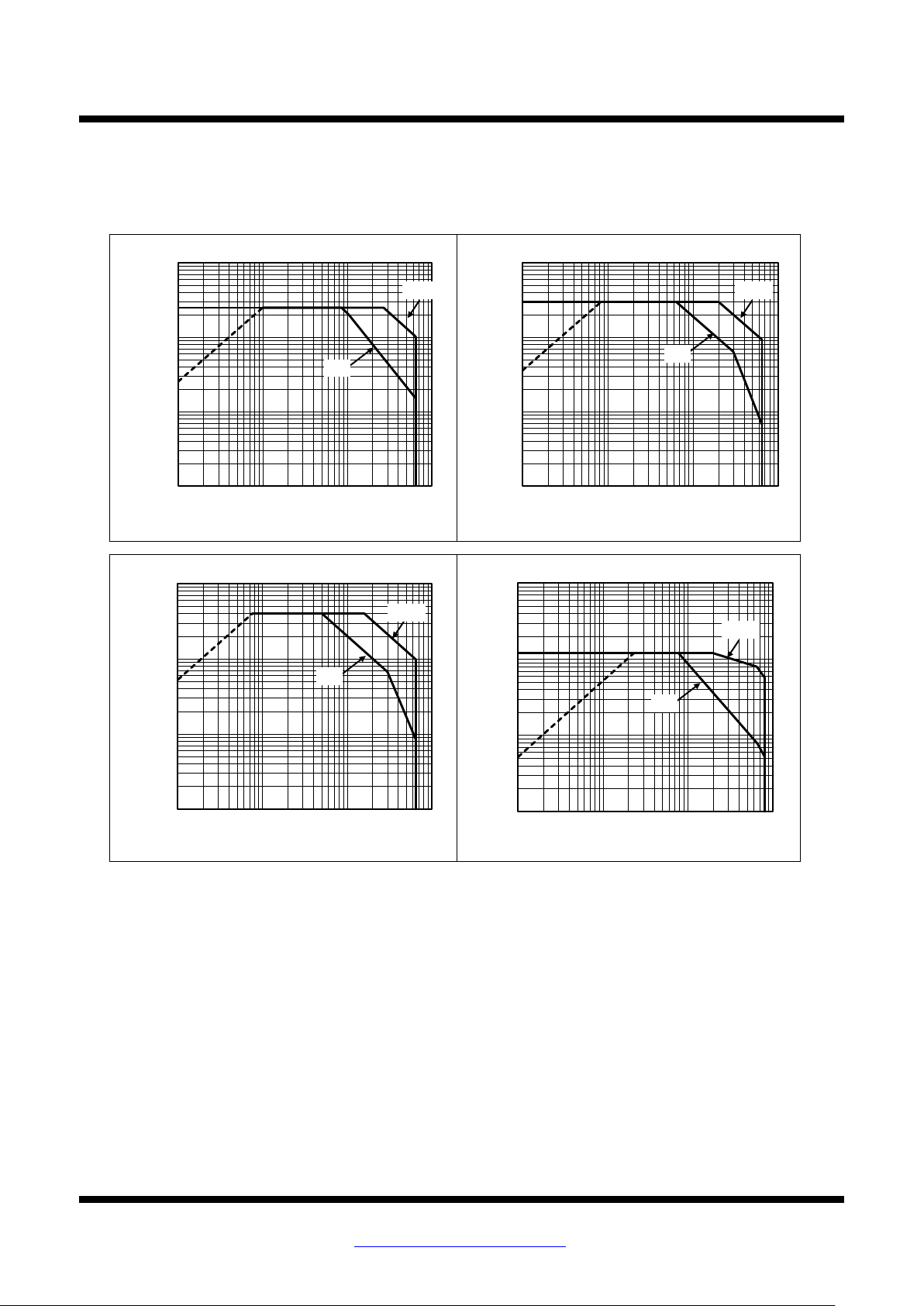
3. Performance Curves
3.1 Derating Curves
100
80
60
40
20
0
0 25 50 75 100 125 150
Channel Temperature, Tch (°C)
Figure 3-1. SOA Temperature Derating Coefficient
Curve
100
80
60
40
20
Temperature Derating Coefficient (%)
AS
0
E
Figure 3-2. Avalanche Energy Derating Coefficient
25 50 75 100 125 150
Channel Temperature, Tch (°C)
Curve
3.2 Ambient Temperature versus Power Dissipation Curve
1.6
1.4
1.2
(W)
1
D1
0.8
0.6
0.4
Power Dissipation, P
0.2
0
0 20 40 60 80 100 120 140 160
Ambient Temperature, TA(°C )
Figure 3-3. Ambient Temperature Versus Power
Dissipation Curve
STR-A6000-DSJ Rev.4.4 SANKEN ELECTRIC CO., LTD. 6
Mar. 13, 2015 http://www.sanken-ele.co.jp/en
© SANKEN ELECTRIC CO., LTD. 2008
STR-A6000 Series
• STR-A6051M
• STR-A6052M
• STR-A6053M
• STR-A6079M
10
Drain Current, I
Drain-to-Source Voltage (V)
0.1ms
1ms
0.1ms
1ms
0.1ms
1ms
0.1ms
1ms
3.3 MOSFET Safe Operating Area Curves
When the IC is used, the safe operating area curve should be multiplied by the temperature derating coefficient
derived from Figure 3-1. The broken line in the safe operating area curve is the drain current curve limited by
on-resistance.
Unless otherwise specified, T
= 25 °C, Single pulse.
A
10
1
(A)
D
0.1
0.01
1 10 100 1000
10
1
(A)
D
0.1
Drain Current, I
1
(A)
D
0.1
Drain Current, I
0.01
1 10 100 1000
Drain-to-Source Voltage (V)
10
1
(A)
D
0.1
Drain Current, I
0.01
1 10 100 1000
Drain-to-Source Voltage (V)
0.01
1 10 100 1000
Drain-to-Source Voltage (V)
STR-A6000-DSJ Rev.4.4 SANKEN ELECTRIC CO., LTD. 7
Mar. 13, 2015 http://www.sanken-ele.co.jp/en
© SANKEN ELECTRIC CO., LTD. 2008
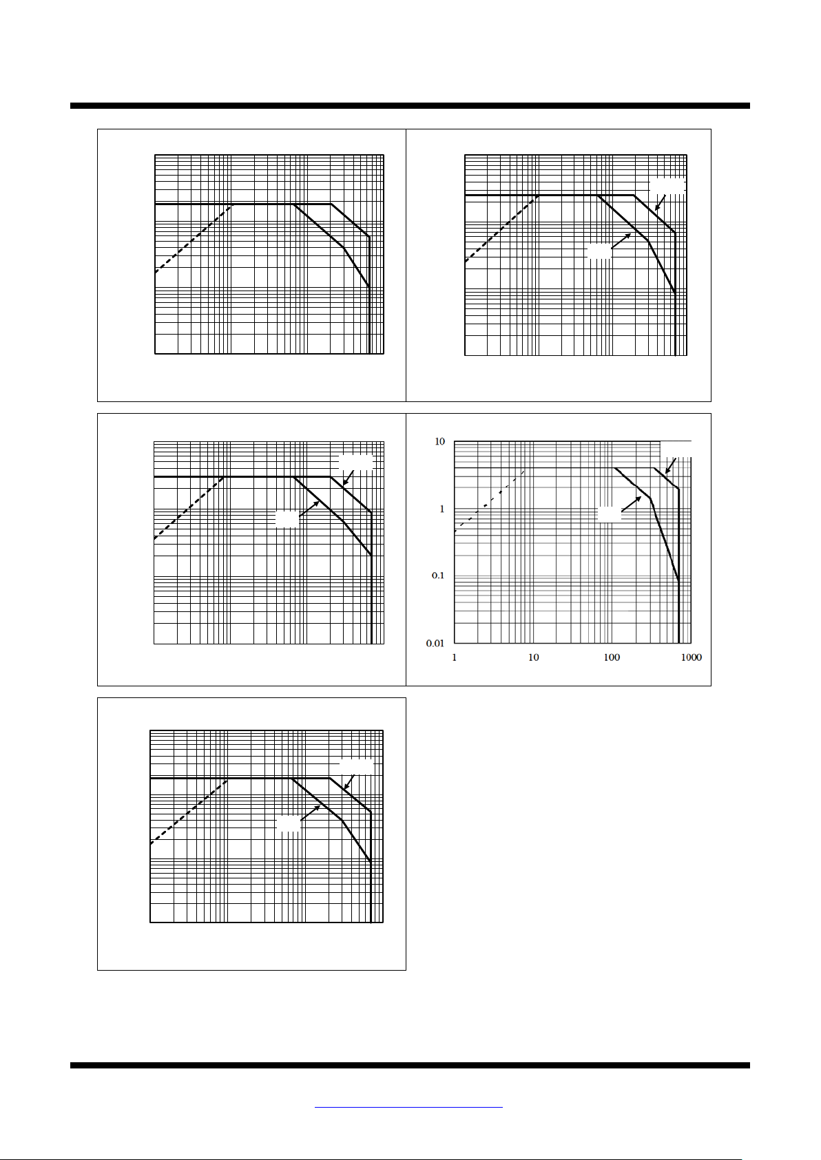
STR-A6000 Series
• STR-A6059H
• STR-A6061H / 61HD
• STR-A6062H / 62HD
• STR-A6063HD
• STR-A6069H / 69HD
10
Drain Current, I
0.1ms
1ms
0.1ms
1ms
0.1ms
1ms
0.1ms
1ms
Drain Current, I
D
(A)
Drain-to-Source Voltage (V)
10
1
(A)
D
0.1
0.01
1 10 100 1000
Drain-to-Source Voltage (V)
10
1
(A)
D
0.1
Drain Current, I
1
(A)
D
0.1
Drain Current, I
0.01
1 10 100 1000
Drain-to-Source Voltage (V)
0.01
1 10 100 1000
Drain-to-Source Voltage (V)
10
1
(A)
D
0.1
Drain Current, I
0.01
1 10 100 1000
Drain-to-Source Voltage (V)
STR-A6000-DSJ Rev.4.4 SANKEN ELECTRIC CO., LTD. 8
Mar. 13, 2015 http://www.sanken-ele.co.jp/en
© SANKEN ELECTRIC CO., LTD. 2008
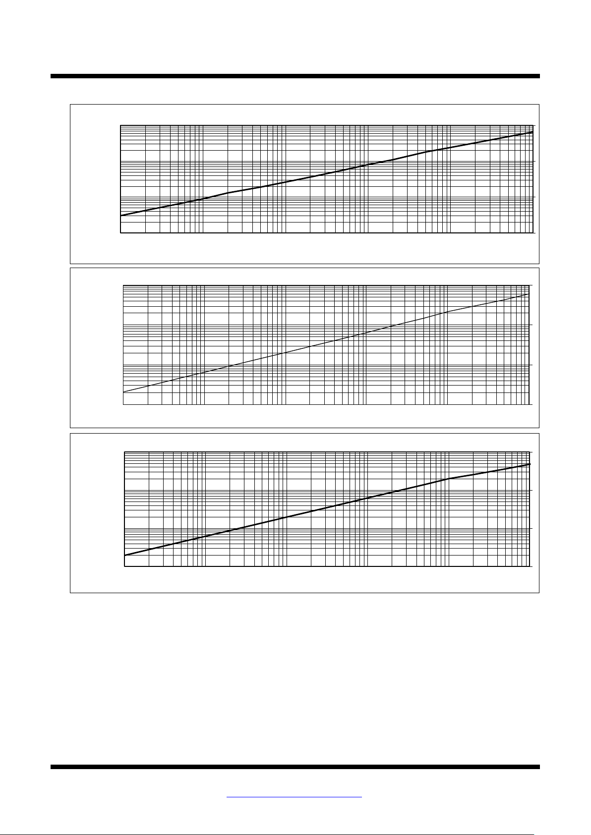
STR-A6000 Series
• STR-A6051M / 61H / 61HD
• STR-A6052M / 62H / 62HD
• STR-A6053M
Transient Thermal Resistance,
Time (s )
1µ 10µ 100µ 1m 10m 100m
1µ 10µ 100µ 1m 10m 100m
1µ 10µ 100µ 1m 10m 100m
10
Transient Thermal Resistance,
3.4 Transient Thermal Resistance Curves
10
1
0.1
θch-c (°C/W)
0.01
1
0.1
θch-c (°C/W)
0.01
10
1
0.1
θch-c (°C/W)
Transient Thermal Resistance,
0.01
Time (s)
Time (s )
STR-A6000-DSJ Rev.4.4 SANKEN ELECTRIC CO., LTD. 9
Mar. 13, 2015 http://www.sanken-ele.co.jp/en
© SANKEN ELECTRIC CO., LTD. 2008
 Loading...