

Page 1

DPR-25
DAB+FM RDS+MW DIGTAL RECEVIER
CONTENTS
Specification ………………………………………………………………………………………………………2-5
Block Diagram ………………………………………………………………………………………………………6
Alignment Instructions…………………………………………………………………………….………………7-11
Test Points Disgram…………………………………………………………………………….……….……………12
Main PCB Top View…………………………………………………………………………….……….……………13
Main PCB Bottom View.………………………………………………………………………….……..………..…..14
LCD PCB Top View……………………………………………………………………………….………….……15
LCD PCB Bottom View……………………………………………………………………………………………16
PCB Top View…………………………………………………………………………….……….……………17
PCB Bottom View…………………………………………………………………………….……….……………18
Wiring Diagram..….………………………………………….………………….….……………..……….19
Troubleshooting Flow Chart..….………………………………………….……………….….……………..……20-21
Electrical Parts List………………………………………………………………………………....……………22-25
Mechanical Parts List……………………………………………………………………….……….…………….26-27
Exploded Views.…………………………………………………………………………….…………….……………28
IC Circuit Block Diagram…………………………………………..…………….………………………………29-38
IC and Transistor Voltage Chart….……………………………..…………………………….…………………39-43
Semiconductor Lead Identifications……………………………………………………………………..……..…44
MAIN Schematic Diagram……………………………………………………………………………………………45
LCD Schematic Diagram………………………………………………………………..……………………..… …46
Page 2

SPECIFICATION
FM. ELECTRICAL PERFORMANCE
Model: DPR-25 Brand:SANGEN
Temp: °C
R.H.: % Date: 2005/9/2
Condition Value Test no.
Test Item
Unit
Input Output freq Nom. Lim 1. 2.
Tuning Range S/N=6dB
Min 87.5
MHz
Max 108
Intermediate freq. S/N=6dB 10.7
Max. Sensitivity S/N=6dB
Usable Sensitivity S/N=30dB
90MHz
98MHz
106MHz
90MHz
98MHz
106MHz
12
12
12
18
18
18
±0.05
18
18
18
24
24
24
MHz
dBu
dBu
Image Rejection S/N=6dB 106MHz 24 18 dB
Stereo Ind Sens. S/N=6dB 106MHz 22 26 dB
I.F. Rejection S/N=6dB 90MHz 60 dB
3db Limiting 80dBu 18 24 dBu
Min. output 1.5 3 mV
Auto Scan 22 28 dBu
S/N (1mV) 46 40 dB
Current Consumption R. O. 160 180 mA
Am. Suppression (1mV) 32 26 dB
Stereo Separation(lkHz) 26 20 dB
Audio fidelity
75kHz/or 50kHz
(-3dB W/pre emphasis)
60dBu
98MHz
100 200 Hz
10K 8K Hz
Output Power(75KHz dev.) 10%T.H.D. 1000 700 mW
T. H. D. (75KHz dev.) 1 3 %
Over load capacity 10%T. H.D.
100 90 dBu
90MHz
Calibration S/N=6dBu
98MHz
KHz
106MHz
Lowest Batt. Volt. 60dBu 98MHz 6.3 6.7 V
Supply Voltage: DC 9V
Remark:
R.O.: 50mW
Load: 8 Ohm
Modulation: 1KHz Mod./22.5KHz Dev.
Approved by Released/Tested by
( )首件產品 ( )客戶抽測:
( )成品 ( )例行抽測 ( )業務樣品:
( )半成品( )新機種 ( )工程變更:
2
Page 3

SPECIFICATION.
Model: DPR-25
MW. ELECTRICAL PERFORMANCE
Brand: SANGEAN
Temp: °C
R.H.: % Date: 2005/9/2
Condition Value Test no.
Test Item
Unit
Input Output freq Nom. Lim 1. 2.
Tuning Range
Min 522
KHz
Max 1710
Intermediate freq. S/N=6dB Min 450
Max. Sensitivity S/N=6dB
Usable Sensitivity S/N=20dB
603KHz
999KHz
1404KHz
603KHz
999KHz
1404KHz
46
42
42
56
54
54
±2
56
54
54
62
60
60
KHz
dBu/m
dBu/m
Image Rejection S/N=6dB 1404KHz 36 30 dB
I.F. Rejection S/N=6dB 603KHz 50 40 dB
Selectivity(±10KHz)
S/N=6dB 32 26 dB
Bandwidth(-6dB) S/N=6dB 6-11 KHz
T. H. D. 74dBu/m 2 4 %
Lowest Batt. Volt. 74dBu/m 6.3 6.7 V
Hum Modulation
Auto. Scan. Stop. Sens. 56 62
100dBu/m
dB
dBu/m
Current Consumption 74dBu/m 160 180 mA
999KHz
Tone Action (3KHz) 74dBu/m dB
Freq. Response
(-6dB)
74dBu/m
100 200 Hz
2500 1800 Hz
Output Power 80% Mod. 10%T.H.D. 1000 700 mW
Over load capacity 80%mod. 10%T. H.D. 100 90
A. G. C. F. O. M.
100dBu/m
46 40 dB
dBu/m
S/N Ration 74dBu/m 40 34 dB
Whistle Modulation 74dBu/m 2IF/3IF 15 %
Supply Voltage: DC 9 V R.O.: 50mW Load: 8 Ohm
Remark:
Modulation: 1KHz/30% Mod
Approved by Released/Tested by
( )首件產品 ( )客戶抽測:
( )成品 ( )例行抽測 ( )業務樣品:
( )半成品( )新機種 ( )工程變更:
3
Page 4

SPECIFICATION.
DAB(BAND
Model: DPR-25 Brand: SANGEAN
Ⅲ)
ELECTRICAL PERFORMANCE
Temp: °C
R.H.: % Date: 2005/9/2
Test Item Condition CH Limit Typical
Min 5A CH
RF Freq. Range
Max 13F CH
Fc : -70 dBm (W anted channel)
Adjacent Channel
Selectivity
Fi : ≧ -38 dBm
(Unwanted channel)
10A 30 33 dB
(Measurement to EN50248)
Fc : -70 dBm (W anted channel)
Fi : ≧ -25 dBm
Far-off Selectivity
FM 75Khz/dev. Fc ±5MHz
10A 43 53 dB
(Unwanted channel)
(Measurement to EN50248)
5A -87 -90 dBm
Sensitivity
Without pop noise
10A -88 -91 dBm
12B -88 -91 dBm
13F -87 -90 dBm
Test no.
Unit
1. 2.
S/N Ratio Without pop noise 10A 50 56 dB
Max. input Signal : Without pop noise 10A -10 0 dBm
5A -90 -92 dBm
Acquisition
Selectivity
(Measurement to EN50248)
10A -92 -94 dBm
12B -92 -94 dBm
13F -90 -92 dBm
Output Power
1kHz
10%T.H.D. 1000 700 mW
T. H. D. 1 3 %
Low battery
Indication on
FREQ
RESPONSE
10A 6.7 6.7 V
AT CHANNEL 10A CHANGE
SERVICE AF
125H
Z
8KHZ +4 +7 dB
+4 +7 dB
Supply Voltage:
DC:9V
Channel
Freq.( MHz)
R.O. : 50mW Load: 8 Ohm Modulation :1kHz
Channel Freq.( MHz) Channel Freq.( MHz)
5A 174.928 10A 209.936 12B 225.648
13F 239.200
( )The head of product
( )Finished Product
( )Semi-finished Product
( )New Model
( )Client Spot Check
( )Routine Spot Check
( )Engineering Modify
( )Business Sample
Approved by Released/Tested by
4
Page 5
Model: DPR-25
SPECIFICTION.
AUX-IN ELECTRICAL PERFORMANCE
Brand: ALL
Temp: 25 ℃
R. H. : 75 % Date: 2005/9/2
Test Item
Output Power
AUX IN
Dynamic Range
I/S (Input Sensitivity)
DISTORTION
MIN OUTPUT
S/N RATIO
Frequency Response
Condition
Value Test No.
Input Output Freq. Nom. Lim. 1. 2.
AUX IN=0.5V/1KHz
THD=10%
1 0.7
Output=R.0 (ATT=0)
THD=3%
1 05
AUX IN=100Hz
AUX IX=100Hz,ATT=0
OUT= 0.5W
130 ±30
Volume=MAX
AUX IN =I/S 1KHz
OUT=R.O
AUX IN =I/S 1KHz
Volume=MIN
AUX IN =I/S 1KHz&GND
OUT=R.O
AUX
IN=0.5V/1KHz
OUT=50mW=0dB
100
10K 8 4
0.1 0.4
0.7 2
65 55
10 6
Unit
W
V
mV
%
mV
dB
dB
AUX IN =I/S 1KHz 130 ±30
LINE OUT LEVEL
(REC OUT IMPD=47K)
FM DEV=22.5K@1KHz 150/ ±30
Supply Voltage: DC 9 V R.O.: 50mW Load: 8 Ohm
Remark:
Approved by Released/Tested by
( )首件產品 ( )客戶抽測:
( )成品 ( )例行抽測 ( )業務樣品:
( )半成品( )新機種 ( )工程變更:
mV
Modulation:
1KHz/30% Mod
5
Page 6
Q15
Q17
AUX
BLOCK DIAGRAM
SW
TC4066
LINE
OUT
3D
PT2386
DC / DC
15V
DAB
Pre-AMP
Tuner
Q4
Q23
PLL & LPF
TA2149
TC9257
RDS
BU1924
Q5
Q6
3DSW
Main-AMP
AN7142
DC / DC
3.3V
DC / DC
5V
6V
REG
FLIP-FLIP
TC4013
POWKEY
u-COM
TMP87EP26F
KEY
Q10
Q27
5V
REG.
9V
REG.
Q22
Q19
DC JACK
9-14V
6
Page 7
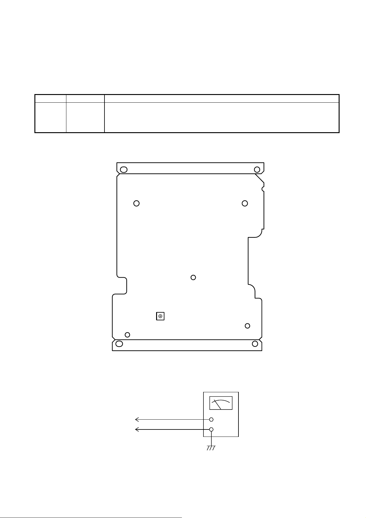
ALIGNMENT INSTRUCTIONS
1. ALIGNMENT FOR AM/LW IF
a. Required Instruments:
AM IF Sweep Generator with scope
b. Alignment Procedure
Mode Adjustment Procedure
(1) Press the power button to turn on the radio.
(2) Connect the input terminal of AM IF sweep generator in series with a resistor of 1.2KΩ
to the TP1 and TP2.
AM T1
c. Instrument Connection
(3) Connect the RF output terminal of AM IF sweep generator to another test point TP5.
(4) Connect a 100μF electrolytic capacitor to test point TP2 and TP4.
(5) Adjust T1 to have a max. output with a marker frequency of 450 kHz on the sweep
scope.
T1
TP4 TP2
100uF
450KHz Marker
TP1
IN
TP2
1.2KΩ
RF
OUT
2.2KΩ
AM IF Sweep Generator
TP5
7
Page 8
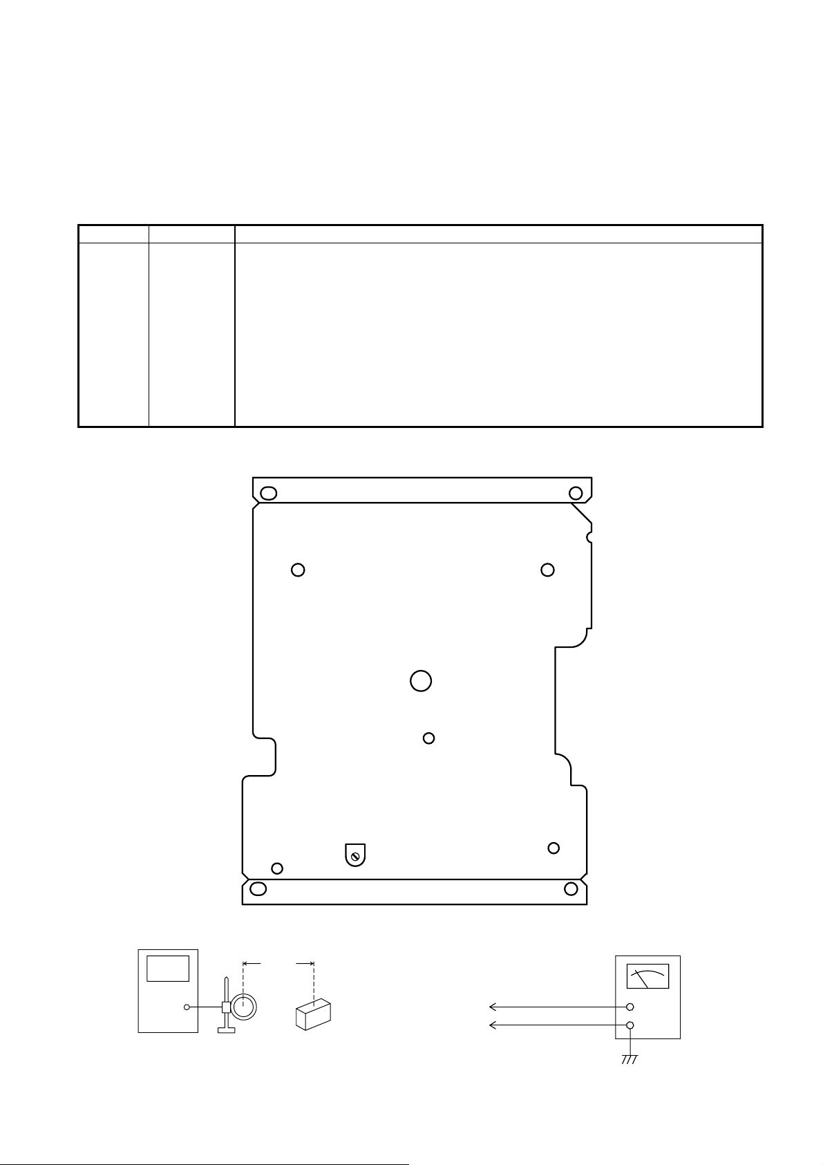
2. ALIGNMENT FOR AM/LW TUNING VOLTAGE RANGE
a. Required Instruments:
DVM
b. Alignment Procedure
Mode Adjustment Procedure
(1) Turn on the radio.
L3
AM
c. Instrument Connection
TC1
(2) Connect the probe of DVM to the test point TP1 and TP2.
(3) Tune the AM frequency to 522 kHz.
(4) Adjust L3 to have a reading of 1.2 ±0.04V.
(5) Tune the AM frequency to 1629 kHz.
(6) Adjust TC1 to have a reading of 7.6 ±0.3V.
TC1
L3
DVM
TP1
TP2
8
Page 9
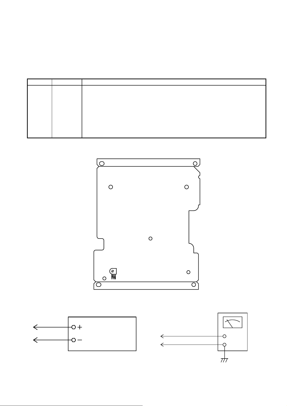
3. ALIGNMENT FOR FM TUNING VOLTAGE
a. Required Instruments
DVM
b. Alignment Procedure
Mode Adjustment Procedure
(1) Turn on the radio.
FM L4
c. Instrument Connection
(2) Connect the probe of DVM to the TP1 and TP2
(3) Tune the FM frequency to 108MHz.
(4) Adjust L4 to have a reading of 8.2V ±0.3V.
L4
TP1
TP2
DVM
9
Page 10
4. ALIGNMENT FOR AM/LW SENSITIVITY
a. Required Instruments
AM Signal Generator
SSVM
b. Alignment Procedure
Mode Adjustment Procedure
(1) Turn on the radio.
(2) Connect a SSVM to the speaker TP7 and TP8 terminals.
(3) Connect an AM signal generator together with standard loop dummy antenna and
feed 30% modulated signal to the AM ferrite bar antenna L12.
TC3
AM
L12
c. Instrument Connection
(4) Tune the generator frequency to 1404 kHz.
(5) Tune the AM frequency to 1404 kHz and adjust TC3 to have a max reading on
SSVM.
(6) Return the generator frequency to 603 kHz.
(7) Tune the AM frequency to 603 kHz and adjust L12 to have a max reading on
SSVM.
(8) Repeat (4) to (7) as necessary to minimize tracking error.
AM Signal Generator
Loop Antenna
60 cm
The radio is located
perpendicularly to
the Loop Antenna
TC3
L12
DVM
TP7
TP8
10
Page 11
5. ALIGNMENT FOR FM TUNING SENSITIVITY
a. Required Instruments
FM Signal Generator (frequency range up to 220 MHz)
SSVM
b. Alignment Procedure
Mode Adjustment Procedure
(1) Turn on radio.
(2) Connect a SSVM to speaker TP7 and TP8.
(3) Connect a FM signal generator to TP10 and TP11.
TC2
FM
c. Instrument Connection
L8
(4) Set the signal generator to 22.5 kHz deviation with 1 kHz modulation.
(5) Always tune the generator frequency to exactly same as the radio band frequency
before adjustment.
(6) Tune the FM frequency to 106MHz and adjust TC2 to have a max audio output.
(7) Tune the FM frequency to 90MHz and adjust L8 to have a max audio output.
(8) Repeat (6) to (7) as necessary to minimize tracking error.
TC2
L8
DVM
TP11
SSG
TP10
11
TP7
TP8
Page 12
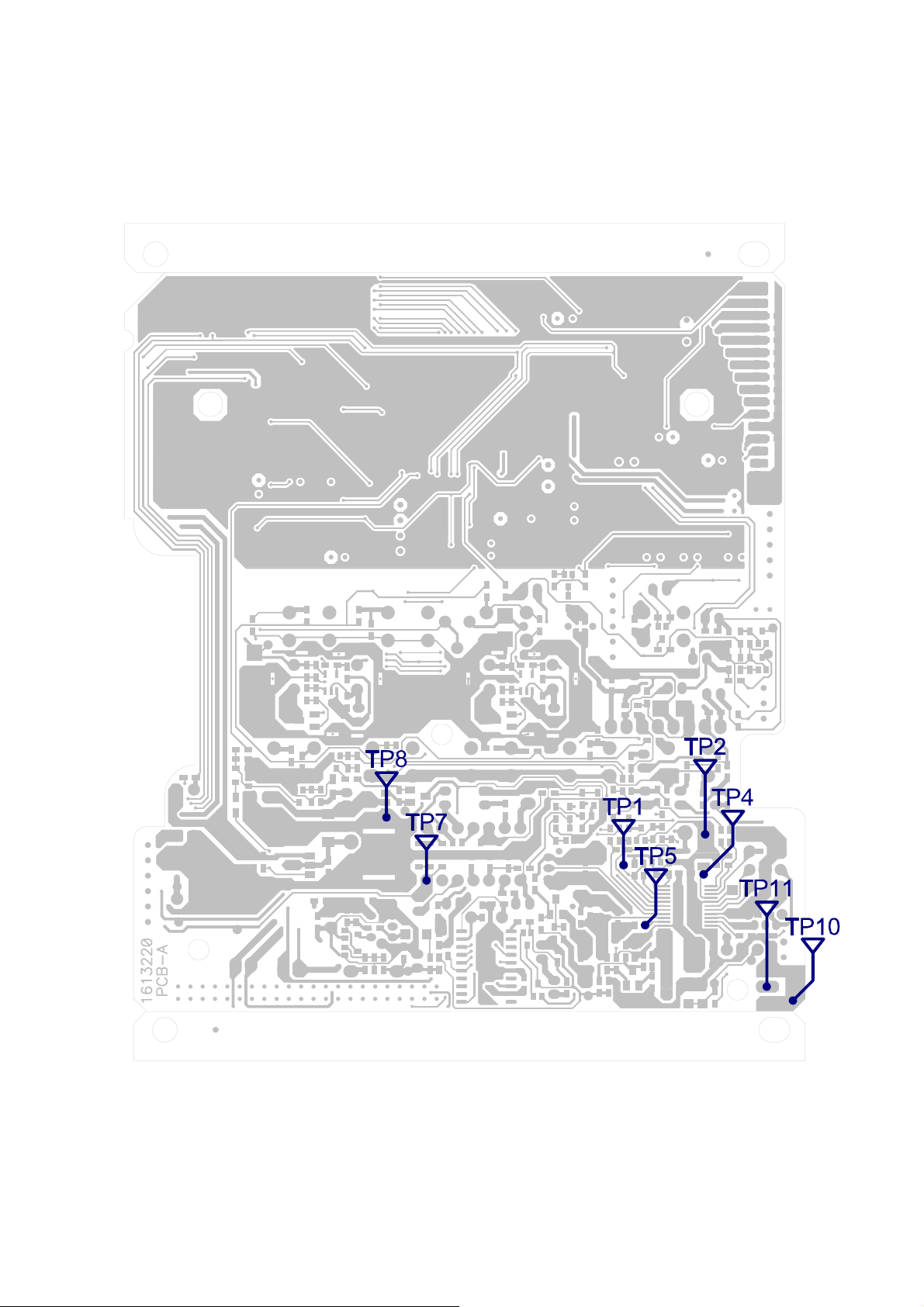
TEST POINTS DIAGRAM
12
Page 13
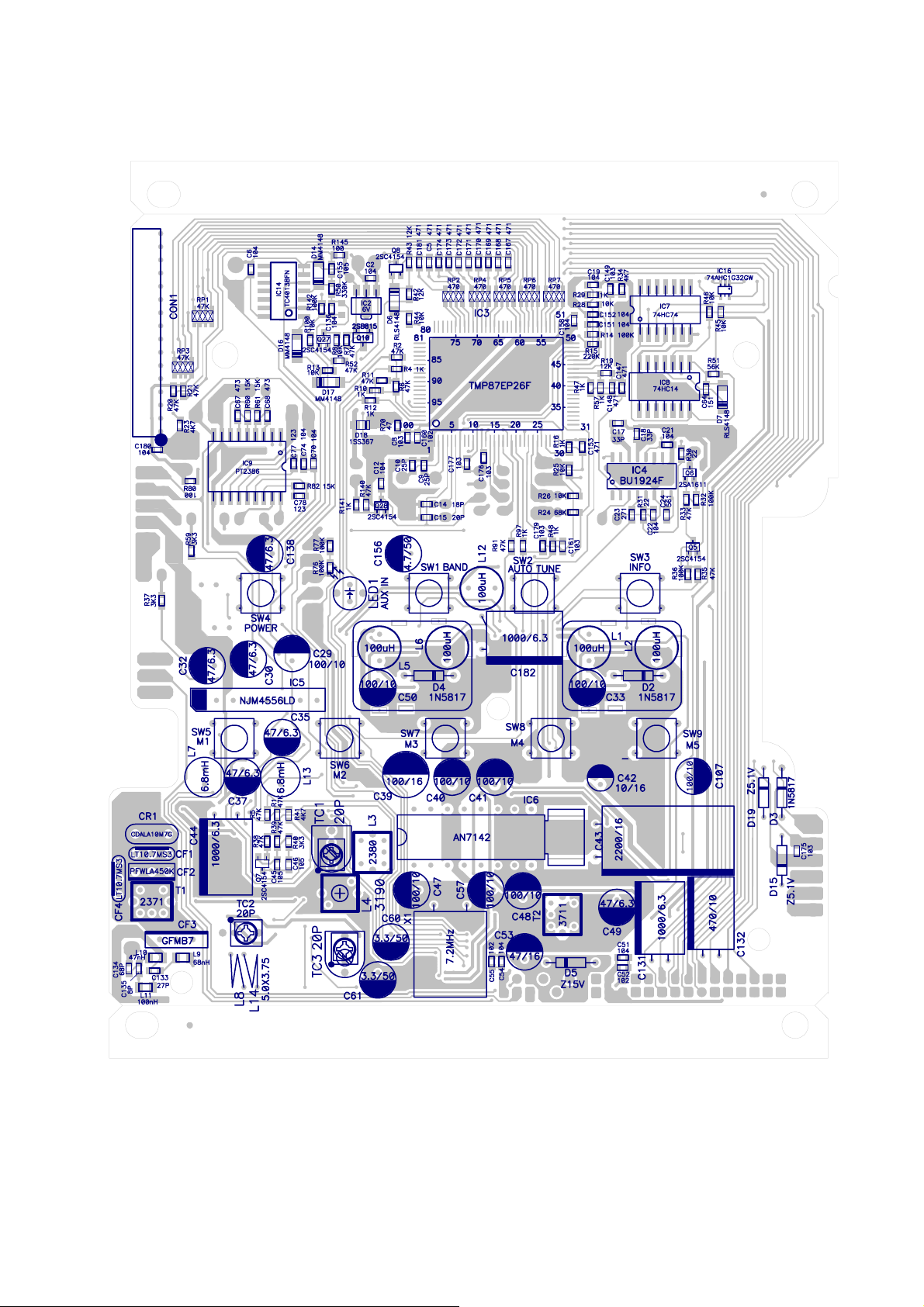
MAIN PCB TOP VIEW
13
Page 14
MAIN PCB BOTTOM VIEW
14
Page 15

LCD PCB TOP VIEW
15
Page 16

LCD PCB BOTTOM VIEW
16
Page 17

PCB TOP VIEW
17
Page 18

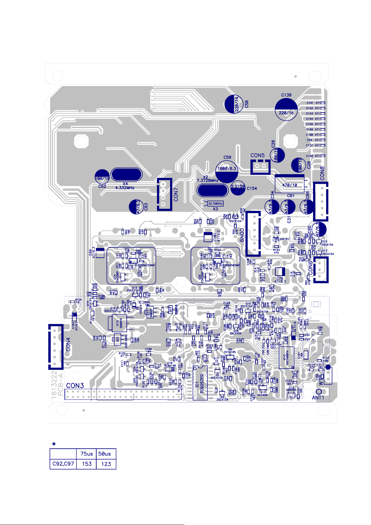
PCB BOTTOM VIEW
18
Page 19

WIRING DIAGRAM
19
Page 20

TROUBLESHOOTING FLOW CHART
( 1 ) DAB can not be turned on
Check whether the pin 18 of DAB
MODULE
exceeds 3.3V DC.
Yes
Check whether the pin1 of DAB
MODULE exceeds 5V DC.
No Check the IC10 and Q14 circuit is
normal.
Then replace the abnormal parts.
No Check the IC13 and Q25 circuit is
normal.
Then replace the abnormal parts.
( 2 ) Weak sensitivity in DAB band
Check the C134, C135, L10, L11
circuit is normal.
Yes
Check the ANT circuit is normal.
No
Check the HPF circuit.
Then replace the abnormal parts.
20
Page 21

( 3 ) Weak sensitivity in FM
Check whether the sensitivity is Yes Check the antenna wire and BPF
recovered if antenna is directly circuit.
connected to the pin 2 of IC12.
Yes
Check whether the IF waveform is
normal.
Yes
Check whether the tuning voltage
is normal.
Then replace the abnormal parts.
No
No
Check the IC12 circuit.
Then replace the abnormal parts.
Check the L4 local oscillator circuit.
Then replace the abnormal parts.
Check whether L8 and TC2 the No
corresponding RF tank circuit are Then replace the abnormal parts.
normal.
Yes
( 4 ) PLL does not work
Check whether the C53 exceeds
15V DC.
Yes
Check whether the circuit of LPF
is normal.
No
No
Check the DC-DC converter circuit.
Then replace the abnormal parts.
Check Q2 and Q3.
Then replace the abnormal parts.
Yes
Check whether the local oscillator
circuit is normal.
Yes
21
Check C121 and D11.
Then replace the abnormal parts.
Page 22

DPR-25
Y
K
ELECTRICAL PARTS LIST
PART NO DESCRIPTION Q'T
1000625 CH LSI ST7066U-OE-B 1 IC 500,
1000770 CH IC TMP87EP26F-4K76 1 IC 3,
1012160-A IC NJM4556AL SIP8 1 IC 5,
1012250 IC AN7142 1 IC 6,
1012320 IC TC4066BP 1 IC 300,
1013260 CH IC TA2149BFN 1 IC 12,
1013460 CH IC XC6365A333MR 1 IC 10,
1013550 CH IC ST7065C (DICE) 1 IC 501,
1013620 CH IC TC 4013BFN 1 IC 14,
1013680 CH IC XC6203E502PR 1 IC 2,
1013990 CH IC BU1924F 1 IC 4,
1014220 CH IC TC9257F 1 IC 1,
1014240 CH IC PT2386 1 IC 9,
1014251/0 CH IC 74HC74D SO14 1 IC 7,
1014261/0 CH IC 74HC14D SO14 1 IC 8,
1014270 CH IC XC6365A503MR 1 IC 13,
1014280 CH IC XC62FP6002PRN 1 IC 11,
1014480-A CH IC BA 09FP TO252-3 1 IC 15,
1014620 CH IC 74AHC1G32GW SOT353 1 IC 16,
1020211 CH TR 2SB815 B7 2 Q 10,17,
1020410-A CH TR 2SA1611-T1-A M6 2 Q 6,9,
1021090 CH TR 2SB1386Q hfe=120 1 Q 22,
1022272 CH TR 2SC4154-G 20 Q 2-5,7,8,11-13,15,16,
18-21,23,24,26-28,
1030280 CH FET FDN358P 2 Q 14,25,
1041190T DIODE 1N5817-T 4 D 2-4,300,
1041220 CH DIODE 1SS367 1 D 18,
1043150-A CH VARICAP KV1450TL-G3/4 1 D 11,
1043160 CH VARACTOR KV1610-2 1 D 9,
1045000T ZENER 1N751A(5.1V)-T 2 D 15,19,
1045020 CH DIODE 1SS314 1 D 8,
1045090 ZENER UZ-15BH 1 D 5,
1046011 CH DIODE MM4148 6 D 6,7,10,14,16,17,
1046180 CH DIODE HBAV99 1 D 12,
1050150 LED RED 3.0x5.1 1 LED1,
1062210 CH LED AMBER 2 D 500,501,
1111350-A BAR ANT & COIL 1350 1 L 12,BAR ANT RF WIRE
1122371 ADJ. COIL 2371 1 T 1,
1122380 ADJ. COIL 2380 1 L 3,
1123190 ADJ. COIL 3190 1 L 4,
1123711 ADJ. COIL 3711 1 T 2,
11301E1G CH WOUND IND.100nHG-A 1 L 11,
1135903S FIXED COIL 6.8mHJ PVC-S 2 L 7,13,
113A2E1G CH WOUND IND.47nHG-A 1 L 10,
113A4E1G CH WOUND 1ND.68nHG-A 1 L 9,
1.15E+64 SP COIL 5.0x1.75Tx0.7 2 L 8,14,
11637K1-3A FIXED COIL 100uHK6φx6.2 5 L 1,2,5,6,12,
1210360 TC 20P RED 3 TC 1-3,
1316125 VR 50KBx2 1 VR 600,
1600700 LCD DPR-25 1 LCD
1613210 PCB D DPR-25 1 PCB D
1613222 PCB A DPR-25 1 PCB A
1613231 PCB E DPR-25 1 PCB E
1621011-A/10-A SPK 2.5" 8Ω 3W 2 SP 300,301,
1630191 SW. 1P2C(E-1)BLACK 1 SW 301,
1631510-A TACT SW 160±50gf9.5mm 9 SW 1-9,
1640350-A JACK EP3.5φ W/SW WHT 2 JK 301,303,
REMAR
22
Page 23

DPR-25
Y
K
ELECTRICAL PARTS LIST
PART NO DESCRIPTION Q'T
1640360-A JACK EP3.5φ N/SW GRY 1 JK 302,
1647100 JACK DC-470AG PBT 2.0L 1 JK 304,
1650150 X'TAL 32.768KHZ 1 X 3,
1650210 X'TAL 7.2MHZ 1 X 1,
1650250 X'TAL 4.332MHZ 1 X 4,
1650570 CRYSTAL 7.3728M±20PPM 1 X 2,
1660341-A FILTER PFWLF450KS2A-A0 1 CF 2,
1664222-A FIL GFMB7-C2-LF 88-108M 1 CF 3,
1664470-A FILTER SFELG10M7HA00-B0 2 CF 1,4,
1664480-A DISCR CDALF10M7GA100A-B0 1 CR 1,
1700130 CNT BASE 2.5x3P 1 CON6,
1700550 CNT BASE 2.5x4P 1 CON7,
1700560 CNT BASE 2.5x5P 1 CON8,
1701086 CNT BASE 2.5x6P 2 CON4,9,
170131G CNT BASE 2x16P-R 1 CON1,
170132G PIN BASE 2x16P-R 1 W 500,
170133M PIN BASE 2x22Px2-S 1 CON3,
1701462 TIP 8x2P-S 2 J 501,502,
1702010 CNT BASE 2.5x2P 1 CON5,
1704830 W/ASS'Y 220(2.5+6P) 1 CON600,
1704950-A W/ASS'Y 100(2.5x2P) 1 CON301,
1704960-A W/ASS'Y 70(2.5x5P) 1 CON303,
1704970-A W/ASS'Y 100(2.5x3P) 1 CON302,
1704980-A W/ASS'Y 100(2.5x4P) 1 CON200,
1705010-A W/ASS'Y 240(2.5+6P) 1 CON300,
1730120 ROTARY ENCODER 1 EN 200,
1900360 W/SPK 200(6+2P) 1 W 301,
1900830-A W/SPK 300(6+2P) R/B 1 W 302,
1900841 DAB/M FS2020 DPR-25 1 MODULE 1,
4110261C CC 102K 50V Y5P 05 1 C 184,
442256PT0 EL 225M 50V 5x11 1 C 154,
443356NT0 EL 335M 50V 4x7 2 C 60,61,
444756NT0 EL 475M 50V 4x7 1 C 156,
441063NT0 EL 106M 16V 4x7 2 C 42,304,
441073JT0 EL 107M 16V 6.3x7 1 C 39,
442271JT0 EL 227M 6.3V 6.3x7 1 C 300,
442273KT0 EL 227M 16V 8x11.5 2 C 58,139,
444772QT0 EL 477M 10V 8x9 1 C 302,
441081KT0 EL 108M 6.3V 8x11.5 4 C 44,59,131,182,
4900306T0 EL 477M 10V 6.3x11 3 C 81,132,301,
4900316S EL 228M 16V 10x20 1 C 43,
4B47533 CH TA 475M 16V 3.2x1.6 1 C 87,
4B47612 CH TA 476M 6.3V 3.2x1.6 1 C 183,
4C47615 CH TA 476M 6.3V 3.5x2.8 3 C 69,76,102,
4H47611T0 EL 476M 6.3V 5x7 11 C 30-32,34,35,37,49,63
,65,66,138,
4H47631T0 EL 476M 16V 5x7 1 C 53,
4H10721T0 EL 107M 10V 5x7 12 C 26,28,29,33,40,41,47
,48,50,57,62,107,
5002001 CH CC 020C 50V NPO-C 1 C 89,
5008001 CH CC 080C 50V NPO-C 1 C 135,
5010261 CH CC 102K 50V X7R-C 18 C 52,55,71,84,91,104,
109,113,116,118,119,
127,160,162,602,604,
606,607,
5010361 CH CC 103K 50V X7R-C 24 C 3,4,7,8,79,80,85,99,
115,123,126,149,157,
REMAR
23
Page 24

DPR-25
Y
K
ELECTRICAL PARTS LIST
PART NO DESCRIPTION Q'T
159,161,175-179,501-
504,
5010471 CH CC 104Z 25V Y5V-C 38 C 1,2,6,12,16,19-22,25
,27,51,54,70,72,74,
75,82,88,93,105,106,
-108,111,112,124,128
130,136,151,152,158,
163,164,180,303,500,
5010557 CH CC 105Z 10V F-C 4 C 45,46,96,155,
5012361 CH CC 123K 50V X7R-C 2 C 77,78,
5015101 CH CC 151J 50V NPO-C 1 C 64,
5015361 CH CC 153K 50V X7R-C 2 C 36,38,
5018001 CH CC 180J 50V NPO-C 2 C 14,94,
5018361 CH CC 183K 50V X7R-C 2 C 165,166,
5020001 CH CC 200J 50V NPO-C 1 C 15,
5022001 CH CC 220J 50V NPO-C 1 C 117,
5022446 CH CC 224Z 25V Y5V-C 3 C 86,98,125,
5025001 CH CC 250J 50V NP0-C 4 C 9,10,11,13,
5027001 CH CC 270J 50V NPO-C 2 C 103,133,
5027101 CH CC 271J 50V NPO-C 1 C 23,
5033001 CH CC 330J 50V NPO-C 2 C 17,18,
5033101 CH CC 331J 50V NPO-C 1 C 95,
5047101 CH CC 471J 50V NPO-C 24 C 5,56,100,137,140-148
,150,153,167-174,181
,
5047331 CH CC 473K 25V B-C 6 C 67,68,83,90,603,605,
5047472 CH CC 474Z 16V Y5V-C 1 C 114,
5056101 CH CC 561J 50V NPO-C 1 C 24,
5068001 CH CC 680J 50V NPO-C 3 C 120,121,134,
5068261 CH CC 682K 50V X7R-C 2 C 92,97,
5068351 CH CC 683K 16V R-C 2 C 600,601,
5210471 CH CC 104Z 25V Y5V-B 1 C 101,
6100104 CH RD 1/16W 2.2J-C 2 R 116,119,
6100116 CH RD 1/16W 22J-C 2 R 30,31,
6100120 CH RD 1/16W 47J-C 5 R 70,75,125,501,509,
6100123 CH RD 1/16W 82J-C 1 R 500,
6100124 CH RD 1/16W 100J-C 5 R 80,133,145,304,305,
6100130 CH RD 1/16W 330J-C 1 R 127,
6100132 CH RD 1/16W 470J-C 7 R 55,72,81,83,99,117,
122,
6100133 CH RD 1/16W 560J-C 3 R 71,131,306,
6100136 CH RD 1/16W 1KJ-C 16 R 4,10,12,16,17,29,47,
48,57,97,109,114,120
,124,135,141,
6100137 CH RD 1/16W 1.2KJ-C 1 R 86,
6100139 CH RD 1/16W 1.8KJ-C 1 R 105,
610013J CH RD 1/16W 2KJ-C 1 R 85,
6100140 CH RD 1/16W 2.2KJ-C 2 R 22,307,
6100142 CH RD 1/16W 3.3KJ-C 3 R 37,40,59,
6100144 CH RD 1/16W 4.7KJ-C 15 R 23,34,41,104,126,128
,502-506,600,601,606
,607,
6100148 CH RD 1/16W 10KJ-C 23 R 8,13,18,25-28,44-46,
58,62,64,67,95,100,
102,107,138,602-605,
6100149 CH RD 1/16W 12KJ-C 5 R 19,42,43,300,302,
610014B CH RD 1/16W 3KJ-C 1 R 84,
REMAR
24
Page 25

DPR-25
Y
K
ELECTRICAL PARTS LIST
PART NO DESCRIPTION Q'T
610014D CH RD 1/16W 4.3KJ-C 1 R 87,
6100150 CH RD 1/16W 15KJ-C 4 R 60,61,82,130,
6100152 CH RD 1/16W 22KJ-C 4 R 54,92,94,144,
6100154 CH RD 1/16W 33KJ-C 2 R 301,303,
6100156 CH RD 1/16W 47KJ-C 32 R 1,2,5,6,7,11,20,21,
33,35,38,39,49,52,56
,65,68,73,74,78,79,
89,91,101,111-113,
118,134,136,140,143,
6100157 CH RD 1/16W 56KJ-C 1 R 51,
6100158 CH RD 1/16W 68KJ-C 3 R 24,88,93,
610015E CH RD 1/16W 43KJ-C 1 R 53,
6100160 CH RD 1/16W 100KJ-C 19 R 14,32,36,63,66,69,76
,77,90,98,103,106,
108,110,123,129,132,
137,142,
6100164 CH RD 1/16W 220KJ-C 1 R 15,
6100165 CH RD 1/16W 270KJ-C 1 R 115,
6100166 CH RD 1/16W 330KJ-C 1 R 50,
6100188 CH RD 1/16W 91KJ-C 1 R 507,
6100194 CH RD 1/16W OJ-C 1 JP 500,
6110194 CH JUMP OJ-B 1 JP 601,
6160136 CH RD 1/10W 1KJ-A 1 R 121,
6500432 CH RP 470Jx4-C 5 RP 2,4-7,
6500456 CH RP 47KJx4-C 2 RP 1,3,
8000040 W/JUMP 10(10)0.6mm 1 W 2-MOUDLE1
8141044 W/PVC 70(6+6)YEL 1 BATT + - 8181010 W/PVC 70(3+3)BLK 1 W 3,
8592750 W/2 270(6+6) R/B 1 W 303,
8601820 W/SHIELD 180(2.5+2.5) 1 ANT1,
8601840 W/SHIELD/2 42(3+3) 1 W 1-MODULE1
REMAR
25
Page 26

Y
K
品固
MECHANICAL PARTS LIST
DPR-25
Ref no PART NO. DESCRIPTION Q'T
1 20P4000 RUBBER KEY HOLDER 1 A3-DPR25-01
2 20P4010 LCD LENS HOLDER 1 A3-DPR25-02
3 20P4020 LCD LIGHT LENS 1 A3-DPR25-03
4 20P4030 LED HOLDER 1 A3-DPR25-04
5 20P4040 SPEAKER HOLDER-L 1 A3-DPR25-05
6 20P4050 SPEAKER HOLDER-R 1 A3-DPR25-06
7 20P4060 BACK SHIELD 1 A4-DPR25-07
8 20P4070 BAR ANT HOLDER 1 A3-DPR25-26
9 2159010 DC/DC SHIELD (UP) 2 A4-800-1217
10 2159020 DC/DC SHIELD (DOWN) 2 A4-800-1218
11 21P4001 LCD HOLDER 1 A3-DPR25-08
12 21P4010 GROUND PLAIN 1 A3-DPR25-09
13 21P4020 A-SHEET PLATE 1 A3-DPR25-31
14 21P4030 BATTERY PLATE(+) 2 A4-DPR25-29
15 21P4040 BATTERY SPRING(-) 2 A4-DPR25-30
16 21P4060 ROD ANT LUG 1 A4-DPR25-33
17 2256000 P.C.B. HEMELON 2
18 2279000 HEMLON CUSHION 5x20x0.8 1
19 22L4070 HEMELON 1
20 22M3010 RIBBON 1 A4-RD15-30
21 2365010 EVA CUSHION 1
22 23P4000 TUNING KNOB SPACER 1 A4-DPR25-27
23 23P4050 PVC FILM 1 A4-DPR25-34
24 23P4060 EVA 85x3 2 A4-DPR25-35
25 23P4070 EVA 24x1.5 2 A4-DPR25-36
26 24M3000 PAD 4 A4-RD15-13
27 24M3010 VR-KNOB SPACER 1 A4-RD15-27
28 24P4000 CONDUCT RUBBER 2 A4-DPR25-11
29 25M5000 EVA 1
30 301P410 FRONT CABINET 1 A1-DPR25-13
31 303P410A BACK COVER(WEEE) 1 A1-DPR25-14
32 304P410 BATTERY COVER 1 A2-DPR25-15
33 304P410-L BATT.CASE-L 1 A2-DPR25-16
34 304P410-R BATT.CASE-R 1 A2-DPR25-17
35 305P410 DIAL WINDOW 1 A2-DPR25-18
36 307P410 TOP COVER 1 A1-DPR25-19
37 310P410 3D/FLAP KNOB 1 A2-DPR25-20
38 311P410 VR KNOB 1 A3-DPR25-21
39 312P410 TUNE KNOB 1 A4-RD15-18
40 313P410 PUSH RUBBER KEY 1 A2-DPR25-23
41 343P410 SPEAKER GRILL 2 A3-DPR25-24
42 344P410 SPEAKER FRAME 2 A2-DPR25-25
43 360M301A ROD ANT 1 A1-RD15-12
44 9062122 SCREW JMB 2.6x12(NI) 1 ROD ANT
45 9090019 SCREW M1.4x4(NI) 17 GROUND PLAIN/TOP COV
46 9101102 SCREW PTP 2X10(NI) 2 FRONT CAB/BACK COVER
47 9103082 SCREW PTP 3x8(NI) 2 BAR ANT HOLDERx2
48 9103142 SCREW PTP 3x14(NI) 5
49 9151062 SCREW PTPW 2x6(NI) 17 JACK PCB/FRONT CABx3
DWG NO. REMAR
LED-11T
ERx5
GROUND PLAIN/BACK CO
VERx3
LCD PCB/FRONT CABx4
TOP COVER/BACK COVER
x5
x2
VR PCB/FRONT CABx2
TUN PCB/FRONT CABx2
26
Page 27

Y
K
MECHANICAL PARTS LIST
DPR-25
Ref no PART NO. DESCRIPTION Q'T
50 9163052 SCREW PTB M3x5(NI) 14 SPK/SPK HOLDERx8
51 9901030 WASHER φ3.3xφ8x0.5T 1
DWG NO. REMAR
A-PCB/FRONT CABx3
BATT.CASE-2/BACK COV
ERx6
FRONT CAB/MODULEx1
SPK HPLDER/FRONT CAB
x6
27
Page 28

Page 29

IC CIRCUIT BLOCK DIAGRAM
1. IC1 – TC9257FG
2. IC2 – XC6203E502PR
29
Page 30

3. IC3 – TMP87EP26F
30
Page 31

4. IC4 – BU1924F
5. IC5 – NJM4556LD
31
Page 32

6. IC6 – AN7141
7. IC7 – 74HC74
32
Page 33

8. IC8 – 74HC14
9. IC9 – PT2386
33
Page 34

10. IC10 – XC6365A333MR
11. IC11 – 6002P
34
Page 35

12. IC12 – TA2149BFN
13. IC13 – XC6365A503MR
35
Page 36

14. IC14 – TC4013BFN
15. IC15 – BA09FB
36
Page 37

16. IC16 – 74AHC1G32GW
17. IC300 – TC4066BP
37
Page 38

18. IC500 – ST7066U
19. IC501 – ST7065C
38
Page 39

IC AND TRANSISTOR VOLTAGE CHART
IC1 – TC9257 IC2 – 6002PC
PIN DAB FM AM PIN DAB FM AM
1
2
3
4
5
6
7
8
9
10
PIN DAB FM AM
IC4 – BU1924
0 2.96 2.70
0 2.93 2.93
0 5.06 5.10
0 5.06 5.10
0 0 0
0 0 0
0 0.89 0.37
0 0 0
0 0 0
0 0 5.77
11
12
13
14
15
16
17
18
19
20
0 0 0
0 5.76 5.79
0 2.88 2.92
0 0 0
0 0 0
0 2.86 2.88
0 5.67 0
0 0 0
0 0.35 0.90
0 0.94 0.94
IC5 – NJM4556LD
PIN DAB FM AM
PIN DAB FM AM
5.05 5.06 5.06
1
8.12 8.26 8.28
2
3
0 0 0
IC6 – AN7142
PIN DAB FM AM
1
2
3
4
5
6
7
8
9
10
11
12
13
14
15
0 2.40 0
0 2.41 0
0 2.45 0
0 2.42 0
0 4.56 0
0 0 0
0 0 0
0 2.43 0
0 0 0
0 0 0
0 0 0
0 4.67 0
0 1.86 0
0 2.24 0
0 0 0
3.00 2.98 2.99
1
3.00 2.98 2.99
2
2.99 2.98 2.99
3
4
5
6
7
8
0 0 0
2.99 2.97 0
3.00 2.98 2.99
3.00 2.98 2.99
6.02 5.99 6.02
1
2
3
4
5
6
7
8
9
10
11
12
13
14
15
0 0 0
1.28 1.20 1.25
0 0 0
0.63 0.60 0.61
7.92 8.42 8.31
0 0 0
4.32 4.35 4.37
0 0 0
0 0 0
4.37 4.39 4.41
8.15 8.20 8.24
7.87 8.21 8.15
0.63 0.62 0.63
0 0 0
1.28 1.20 1.24
16
0 2.33 0
8.05 8.06 8.11
16
39
Page 40

IC3 – TMP87EP26F
PIN DAB FM AM PIN DAB FM AM PIN DAB FM AM PIN DAB FM AM
1
2
3
4
5
6
7
8
9
10
11
12
0 0 0
2.35 2.28 2.29
2.04 2.04 2.06
4.47 4.45 4.47
2.23 2.23 2.24
1.79 1.76 1.77
0 0 0
0 0 0
0.22 0.36 0.29
0 0 0
4.99 4.98 4.99
4.97 4.98 4.98
26
27
28
29
30
31
32
33
34
35
36
37
0 2.33 0
0 0 0
0 0 0
0 0 0
0 0 0
0 0 0
0 0 0
0 0 0
0 0 0
0 0 0
0 0 0
0 0 0
4.57 4.54 4.57
51
3.17↓
52
3.17↓
53
3.17↓
54
3.17↓
55
3.17↓
56
4.91↓
57
4.17↓
58
59
60
61
62
0 0 0
4.94 4.95 4.96
0 0 0
0 0 0
0 0
4.95 4.96
0 0
4.95 4.96
4.95 4.96
4.95 4.96
4.95 4.96
76
77
78
79
80
81
82
83
84
85
86
87
0 0 0
0 0 0
0 0 0
0 0 0
0 0 0
0 0 0
0 0 0
0 0 0
0 0 0
0 0 0
0 0 0
0 0 0
13
14
15
16
17
18
19
20
21
22
23
24
25
0 0 0
0 0 0
0 0 0
0 0 0
0 0 0
4.54 4.51 4.54
0 4.54 4.56
4.57 0 0
0 0 0
4.56 4.53 4.56
0 0 0
4.81 4.78 4.81
4.81 0 0
38
39
40
41
42
43
44
45
46
47
48
49
50
0 0 0
0 0 0
0 0 0
0 0 0
0 2.45 0
0 4.08 4.07
3.86 3.88 3.88
2.53 2.56 2.57
4.81 4.79 4.82
4.81 4.78 4.81
4.81 4.79 4.82
0 0 0
0 0 0
63
64
65
66
67
68
69
70
71
72
73
74
75
0 0 0
0 0 0
0.18 0.41 0.35
4.93 0 0
4.89 0 0
1.32 0 0
1.32 0 0
1.32 0 0
1.27 0 0
1.27 0 0
2.85 0 0
0 0 0
0 0 0
88
89
90
91
92
93
94
95
96
97
98
99
100
0 0 0
0 0 0
0 0 0
0 0 0
0 0 0
0 0 0
0 0 0
0 0 0
0 0 0
0 0 0
0 5.07 5.09
0 5.07 5.09
4.54 4.54 4.57
40
Page 41

IC7 – 74HC74
PIN DAB FM AM PIN DAB FM AM
1
2
3
4
5
6
7
IC8 – 74HC14
PIN DAB FM AM PIN DAB FM AM
1
2
4.95 0 0
3.34 0 0
0 0 0
4.95 0 0
4.92 0 0
0 0 0
0.40 0 0
4.92 0 0
0 0 0
4.95 0 0
8
4.95 0 0
9
0.45 0 0
10
0.46 0 0
11
0.43 0 0
12
0.45 0 0
13
4.95 0 0
14
8
9
4.95 0 0
0.45 0 0
IC10 – XC6365A333MR
PIN DAB FM AM
4.72 8.08 8.12
1
7.84 8.08 8.12
2
3
4
5
IC11 – 6002PC
PIN DAB FM AM
1
2
3
0 0 0
4.51 0 0
3.34 0 0
7.96 8.08 8.12
6.03 6.01 6.02
0 0 0
3
4
5
6
7
PIN DAB FM AM PIN DAB FM AM
1
2
3
4
5
6
IC9 – PT2386
0 0 0
4.95 0 0
0.44 0 0
4.95 0 0
0 0 0
2.92 2.92 2.92
2.92 2.92 2.92
2.94 2.94 2.94
2.94 2.94 2.94
2.94 2.94 2.94
2.93 2.94 2.94
4.95 0 0
10
0.44 0 0
11
4.95 0 0
12
0.45 0 0
13
4.95 0 0
14
10
11
12
13
14
15
0 0 0
6.02 6.02 6.02
5.99 5.99 5.99
2.94 2.92 2.93
2.94 2.94 2.94
2.94 2.94 2.94
IC13 – XC6365A503MR
PIN DAB FM AM
3.19 8.08 8.12
1
7.84 8.08 8.12
2
3
4
5
0 0 0
4.51 0 0
4.99 0 0
IC15 – BA09FP
PIN DAB FM AM
7
8
9
2.94 2.94 2.94
0 0 0
6.02 6.02 6.02
2.94 2.94 2.94
16
2.94 2.92 2.92
17
2.95 2.96 2.96
18
41
7.96 8.12 8.25
1
2
3
0 0 0
8.14 8.08 8.12
Page 42

IC12 – TA2149BFN
PIN DAB FM AM PIN DAB FM AM
1
2
3
4
5
6
7
8
9
10
11
12
0 0 0
0 0.79 0
0 0 1.15
0 5.73 5.95
0 5.96 5.98
0 5.42 5.31
0 5.96 5.98
0 0 0
0 0.80 0.44
0 5.21 5.40
0 1.24 4.52
0 1.26 1.28
13
14
15
16
17
18
19
20
21
22
23
24
0 5.05 0
0 5.21 0
0 0.70 0.71
0 1.09 1.18
0 0.75 0.94
0 4.41 4.40
0 5.15 5.24
0 5.96 5.98
0 5.96 5.98
0 5.96 5.98
0 5.96 5.98
0 5.96 5.98
IC16 – 74AHC1G32GW
PIN DAB FM AM
4.99 4.99 4.99
1
4.98 4.98 0
2
3
4
5
0 0 0
4.70 0 4.71
4.73 0 4.74
IC14 – TC4013BFN
PIN DAB FM AM PIN DAB FM AM
1
2
3
4
5
6
7
IC300 – TC4066BP
PIN DAB FM AM PIN DAB FM AM
1
2
3
4.98 0 4.98
0 0 0
0 0 0
0 0 0
0 0 0
0 0 0
0 0 0
0 0 0
2.03 2.16 2.18
0.35 0.29 0.32
8
9
10
11
12
13
14
8
9
10
0.39 0.17 0.32
0.39 0.16 0.27
0.37 0.16 0.33
0.37 0.16 0.40
5.04 4.95 5.04
0 0 0
5.03 4.96 5.04
0.35 0.32 0.32
0.35 0.32 0.32
2.06 2.19 2.18
4
5
6
7
0.35 0.31 0.32
0.32 0.28 0.25
0.31 0.29 0.28
0 0 0
11
12
13
14
0 0 0
0 0 0
0 0 0
6.01 5.99 6.02
42
Page 43

Transistor
DAB FM AM DAB FM AM DAB FM AM
0 0 0
E
Q2
Q3
Q4
Q5
0 0.53 0.56
B
1.93 4.95 4.37
C
0 0.53 0.56
E
0 0.92 0.96
B
1.93 4.95 4.37
C
0 0 0
E
0 0 0
B
0 0 3.29
C
0 0 0
E
0 0.61 0
B
0 0 4.74
C
4.81 4.79 4.82
E
E
Q11
B
E
Q12
B
E
Q13
B
S
Q14
G
E
0 0 0
0 0 0
4.85 4.84 4.84
C
0 0 0
0 0 0
0.40 0 0
C
0 0 0
0 0 0
0.41 0 0
C
7.85 8.07 8.11
5.13 8.07 8.12
3.46 0 0
D
0 0 0
Q20
Q21
Q22
Q23
0 0 0
E
0 0 0
B
0 0 0
C
0 0 0
E
0 0 0
B
0 0 0.94
C
8.05 8.22 8.26
E
7.34 7.52 7.56
B
8.01 8.20 8.25
C
0 0 0
E
0 0 0.59
B
0 5.04 0
C
0 0 0
E
Q6
Q7
Q8
Q9
Q10
4.77 4.10 4.77
B
0 4.68 0
C
0 0 0
E
0 0 0.61
B
0 5.22 0
C
0 0 0
E
0.64 0.65 0.68
B
0 0 0
C
0 0 0
E
0 0 0
B
0 0 0
C
5.05 6.06 5.05
E
4.37 4.38 4.37
B
5.04 5.05 5.04
C
Q15
B
E
Q16
B
E
Q17
B
E
Q18
B
E
Q19
B
0 0.58 0.60
5.96 0 0
C
0 0 0
0 0 0
0 0 0
C
6.03 6.00 6.02
5.97 5.31 5.33
0 5.94 5.99
C
0 0 0
0 0 0
0.65 0.64 0.66
C
0 0 0
0.65 0.63 0.66
0 0 0
C
Q24
Q25
Q26
Q27
Q28
0 0.35 0.38
B
0 5.38 5.59
C
7.86 8.07 8.11
S
3.35 8.07 8.11
G
5.18 0 0
D
0 0 0
E
0 0.53 0.56
B
0 0.35 0.38
C
0 0 0
E
0.66 0.66 0.66
B
0 0 0
C
0 0 0
E
0 0 0
B
4.47 4.45 4.47
C
43
Page 44

SEMICONDUCTOR LEAD IDENTIFICATIONS
Transistors
C
BE
2SC4154
2SA1611
2SB815
(E:Emitter C:Collector B:Base)
Diodes
C
E
B
2SB1386Q
C
A
A
MM4148
1SS314
1SS367
A
A
ZENER RD15
ZENER RD5.1
C
C
C
C
AA
KV1610S
KV1450
A
A
IN5817
(A:Anode C:Cathode)
C
C
44
Page 45

MAIN SCHEMATIC DIAGRAM
CMP
T1
8
9
VSS3
T2
7
10
VSS1
VSS2
6
11
VDD1
VDD2
5
12
MUX
XIN
4
13
VREF
XOUT
3
14
RDATA
NC
2
15
QUAL
RCLK
1
16
50
49
VSS
BOOT
51
VDD
52
LCD_DB0
53
LCD_DB1
54
LCD_DB2
55
LCD_DB3
56
LCD_DB4
57
LCD_DB5
58
LCD_DB6
59
LCD_DB7
60
LCD_RS
61
LCD_E
62
NC
63
NC
64
NC
65
NC
66
DAB_REMOTE
67
LCD_LCD_LRS
68
DAB_DAT0
69
DAB_DAT1
70
DAB_DAT2
71
DAB_DAT3
72
DAB_DAT4
73
DAB_DAT5
74
DAB_DAT6
75
DAB_DAT7
76
SCL
77
SDA
78
REQ
79
NC
80
NC
NC
NC
81
41
40
44
47
43
42
46
OLT
AD-K1
84NC85NC82NC83
CLT39SLT
AD-K245AD-K348VAREF
PWR-DET
RDS-DATA
STEREO-DET
NC
NC
NC
87
32
31
38
37
BUCK35BUS2
CEE-33BUS034BUS136BUS3
96
VLC97DATA
RES-
30
CD-RW
29
NC
28
DAB_LCD_PE
27
RDS-CLK
26
VOL-CLK
25
VOL-DATA
24
AUX
23
POWER-EN
22
VOL-STB
21
DAB
20
TUNE
19
LIGHT
18
(WAIT)
17
SO2)
16
(SI2)
15
(SCK2-)
14
TIME-OFF
13
POW-ON-DET
12
AD-DET
11
MUTE-EN
10
REMOTE
9
NC
8
TEST-
7
XTIN
6
XTOUT
5
RESET-
4
XIN
3
XOUT
2
VSS
1
VDD
CLK
PRD
98
99
100
D-OPEN
D-CLOSE
NC
95NC92NC89NC86
94NC90NC91NC88
93
45
Page 46

LCD SCHEMATIC DIAGRAM
46
 Loading...