

Samsung ZV10 Service Manual
UMTS TELEPHONE
SGH-ZV10
UMTS TELEPHONE
CONTENTS
1. Specification
2. Circuit Description
3. Exploded Views and Parts List
4. Electrical Parts List
5. Block Diagrams
6. PCB Diagrams
7. Flow Chart of Troubleshooting
This Service Manual is a property of Samsung Electronics Co.,Ltd.
Any unauthorized use of Manual can be punished under applicable
International and/or domestic law.
ⓒ
Samsung Electronics Co.,Ltd. October. 2005
Printed in Korea.
Code No.: GH68-08595A
BASIC.
1. Specification
1-1. GSM General Specification
EGSM900 DCS1800 PCS1900 W-CDMA
Freq.
Band[MHz]
Uplink/Downlink
ARFCN range
Tx/Rx spacing 45MHz 95MHz 80MHz 190MHz
Mod. Bit rate/
Bit Period
Time Slot
Period/Frame
Period
Modulation 0.3GMSK 0.3GMSK 0.3GMSK
MS Power 33dBm~5dBm 30dBm~0dBm 30dBm~0dBm 24dBm ~ - 50dBm
Power Class
890~915
935~960
0~124 &
975~1023
270.833kbps
3.692us
576.9us
4.615ms
4
(max +33dBm)1(max +30dBm)1(max +30dBm)
1710~1785
1805~1880
512~885 512~810
270.833kbps
3.692us
576.9us
4.615ms
1850~1910
1930~1990
270.833kbps
3.692us
576.9us
4.615ms
1920~1980
2110~2170
UL:9612~9888
DL:10562~10838
3.84Mcps
Frame length : 10ms
QPSK
HQPSK
3
(max +24dBm)
Sensitivity -102dBm -100dBm -100dBm -106.7dBm
TDMA Mux 8 8 8
Cell Radius 35Km 2Km 2Km 2Km
1-1
SAMSUNG Proprietary-Contents may change without notice
This Document can not be used without Samsung's authorization
Specification
1-2. GSM TX power class
TX Power
control level
533±2dBm
631±2dBm
729±2dBm
827±2dBm
925±2dBm
10 23±2 dBm
11 21±2 dBm
GSM900
TX Power
control level
030±3dBm
128±3dBm
226±3dBm
324±3dBm
422±3dBm
520±3dBm
618±3dBm
DCS1800
TX Power
control level
030±3dBm
128±3dBm
226±3dBm
324±3dBm
422±3dBm
520±3dBm
618±3dBm
PCS1800
12 19±2 dBm
13 17±2 dBm
14 15±2 dBm
15 13±2 dBm
16 11±3 dBm
17 9±3dBm
18 7±3 dBm
19 5±3 dBm
716±3dBm
814±3dBm
912±4dBm
10 10±4 dBm
11 8±4dBm
12 6±4 dBm
13 4±4 dBm
14 2±5 dBm
716±3dBm
814±3dBm
912±4dBm
10 10±4 dBm
11 8±4dBm
12 6±4 dBm
13 4±4 dBm
14 2±5 dBm
15 0±5 dBm
1-2
15 0±5 dBm
SAMSUNG Proprietary-Contents may change without notice
This Document can not be used without Samsung's authorization

2. Circuit Description
2-1. SGH-ZV10 RF Circuit Description
- Antenna Switch Module (RFS103)
The antenna switch module allows multiple operating bands and modes to share the same antenna. A common
antenna connects to one of seven paths: 1) UMTS-2100 Rx/Tx, 2) EGSM-900 Rx, 3) EGSM-900 Tx, 4) DCS-1800
Rx, and 5) DCS-1800 Tx. 6) PCS-1900 Tx, 7) PCS-1900 Rx, UMTS operation requires simultaneous reception and
transmission.
- Filter
To convert Electromagnetic Field Wave to Acoustic Wave and then pass the specific frequency band.
· GSM Rx FILTER (F100)→For filtering the frequency band between 925 ~ 960 MHz.
· DCS Rx FILTER (F101)→For filtering the frequency band 1805 and 1880 MHz.
· PCS Rx FILTER (F102)→For filtering the frequency band 1930 and 1990 MHz.
· WCDMA Rx FILTER (F200)→For filtering the frequency band 2110 and 2170 MHz.
· WCDMA Tx FILTER (F201)→For filtering the frequency band 1920 and 1980 MHz.
- VCTCXO (TCX200)
To generate the 19.2MHz reference clock to drive the logic and RF.
-Duplexer(F203)
A duplexer splits a single operating band into receive and transmit paths.
- WCDMA PAM (PAM201)
This is a key component in the transmitter chain and must complement the RTR6200 IC precisely; jointly they
dominate the UMTS transmitter performance characteristics. Parameters such as gain, output power level, ACLR,
harmonics, Rx-band noise, and power supply current are critical.
- GSM/DCS PAM (PAM102)
The PAM is a key component in any transmitter chain and must complement the rest of the transmitter precisely.
For GSM, DCS, PCS operation, the closed-loop transmit power control functions add even more requirements relative
to the UMTS PA. In addition to gain control and switching requirements, the usual RF parameters such as gain,
output power level, several output spectrum requirements, and power supply current are critical.
- GSM/DCS Dual Tx VCO (VCO101)
The dual Tx VCO outputs, one for EGSM and one for DCS, drive a resistive network that splits the active signal
into two signals: 1) the input to the active PAM – this is the low loss path, and 2) the OPLL feedback signal.
- Dual VCO (VCO201)
The dual-band UHF VCO is a key component within its phase-locked loop; VCO performance directly impacts PLL
and transceiver performance. GSM/DCS Rx/Tx LO & UMTS Rx LO signal is generated from this dual VCO's output.
2-1
SAMSUNG Proprietary-Contents may change without notice
This Document can not be used without Samsung's authorization

Circuit Description
- S1M8691X (U200)
The S1M8691X includes an LNA circuit optimized for UMTS-2100 operation. The LNA is separated from all other
receive functions contained within the S1M8691X receiver IC to improve mixer LO to RF isolation a critical parameter
in the Zero-IF architecture.
- S1M8621X (U615)
The S1M8621X provides the Zero-IF receiver signal path, from RF to analog baseband, for UMTS-2100 applications.
The S1M8621X accepts its UMTS input signal from the handset RF front-end design. The UMTS input is configured
differentially to optimize second-order inter-modulation and common mode rejection performance, and implements
MSM-controlled gain adjustments to extend the receiver dynamic range.
- RTR6250 (U101)
The RTR6250 supports multi-band, multi-mode phones with two receiver signal paths and three transmitter signal
paths:
1) Receiver paths
- EGSM-900
- DCS-1800
- PCS-1900
2) Transmitter paths
- EGSM-900 (using OPLL technique)
- DCS-1800 (using OPLL technique)
- PCS-1900
- UMTS-2100
Numerous secondary functions are integrated on-chip as well:
3) Phase-locked loop circuits
- PLL#1 and an on-chip VCO supports UMTS Tx
- PLL#2 and an external VCO supports EGSM Rx and Tx, DCS Rx and Tx, DCS Rx and Tx and UMTS Rx
4) Transceiver LO generation and distribution circuits
- EGSM-900 Rx and Tx
- DCS-1800 Rx and Tx
- PCS-1900 Rx and Tx
- UMTS-2100 Tx
2-2
SAMSUNG Proprietary-Contents may change without notice
This Document can not be used without Samsung's authorization

Circuit Description
2-2. Baseband Circuit description of SGH-ZV10
2-2-1. PM6650
- Power Management
Ten low-dropout regulators designed specifically for GSM applications power the terminal and help ensure optimal
system performance and long battery life. It provides seven LDO support for 1.375V, 1.8V, 2.6V, 2.85V, 3.0V, 3.3V
while a self-resetting, electronically fused switch supplies power to external accessories. Ancillary support functions,
such as RTC module and RTC charger, Clock Buffer, aid in reducing both board area and system complexity.
SBI BUS serial interface provides access to control and configuration registers. This interface gives full control of
the MSM6250 and enables system designers to maximize both standby and talk times.
Supervisory functions. including a reset generator, an input voltage monitor, and a ADC Conertte support reliable
system design. These functions work together to ensure proper system behavior during start-up or in the event of a
fault condition(low microprocessor voltage, insufficient battery energy, or excessive die temperature).
- TCXO Controller and Buffers
The PM6650 IC includes circuits for controlling the TCXO warm-up and buffering its signal for distribution
throughout the handset. Performance specifications are presented below.
2-2-2. Connector
- LCD Connector
LCD is consisted of main LCD(color 260K TFT LCD) and small LCD(color 65K LCD). Main LCD has 1.8", 176x220
resolution and sub LCD has 1.07", 96x96 resolution. Sub LCD uses STR to improve reflection performance. Chip
select signals in MSM6250, MLCD_CS_N can enable main LCD and SLCD_CS_N can enable small LCD.
MLCD_BL_EN enables white LED of main LCD. MLCD_RESET signal initiates the reset
process of the main LCD. SLCD_RESET signal initiates the Reset process of the small LCD.
-Key
This is consisted of key interface pins among U301, KEY_N(0:4). These signals compose the matrix. Result of
matrix informs the key status to key interface in the U301. Power on/off key is seperated from the matrix. The key
LED use the "VREG_KEY_LED" supply voltage. "HALL_SW" informs the status of folder (open or closed) to the.
- EMI ESD Filter
This system uses the EMI ESD filter, GMF05LC to protect noise from IF CONNECTOR part.
- IF connetor
It is 24-pin connector. They are designed to use VBATT, VF, MSM_TDI, MSM_TDO, MSM_TCK, MSM_TMS,
MSM_TRST, MSM_RTCK, RFR, CTS, JIG_ON, USB_VBUS, RXD, TXD, BOOT_SW and GND. They connected to
power supply IC, microprocessor and signal processor IC.
2-3
SAMSUNG Proprietary-Contents may change without notice
This Document can not be used without Samsung's authorization

Circuit Description
2-2-3. Audio
YMU765 has a built-in amplifier, and thus, is an ideal device for outputting sounds that are used by mobile phones
in addition to game sounds and ringing melodies that are replayed by a synthesizer.
The synthesizer section adopts "stereophonic hybrid synthesizer system" that are given advantages of both FM
synthesizers and Wave Table synthesizers to allow simultaneous generation of up to 32 FM voices and 32 Wave
Table voices. Furthermore, YMU765 has a built-in hardware sequencer that helps to realize complex play without
heavily loading the host CPU. And this device also has a built-in circuit for controlling vibrators and LEDs
synchronizing with play of music. The consumed electric current can be stopped to the minimum by power down
mode when not operating.
The hardware sequence built in this device allows playing of the complex music without giving excessive load to the
CPU of the portable telephones. Moreover, the registers of the FM synthesizer can be operated directly for real time
sound generation, allowing, for example, utilization of various sound effects when using the game software installed
in the portable telephone.
2-2-4. Memory
The signals in the MSM6250 enable two memories. They use volt supply voltage, VREG_MSMP, VREG_MSME
from the PM6650. This system uses SEC's memory, KBE00F005M-F411. It is consisted of 1G bits flash NAND
memory and 512M bits SDRAM memory. It has 16 bit data line, D1[0~15] which is connected to MSM6250.
2-2-5. Camera
The camera module consists of VGA pixel of system LSI(Samsung Techwin), 1/5.8" VGA CMOS image sensor with
an embedded image signal processor. Pixel size is 4.0 um and effective resolution is 640(H) x 480(V).
2-2-6. Irda
This system uses IRDA module, HSDL_32085, Agilent's. It uses two power signals, "VREG_MSMP" for circuit and
"VBATT" for LED.
2-2-7. Bluetooth
This system uses Bluetooth module, LBDA245AN0, Murata's. Chip solution is of Broadcom, BCM2004. It uses a
power signal, "VREG_BT". This system uses Blue-Q interface in that module has RF circuit and base band bluetooth
part is in MSM6250.
2-4
SAMSUNG Proprietary-Contents may change without notice
This Document can not be used without Samsung's authorization
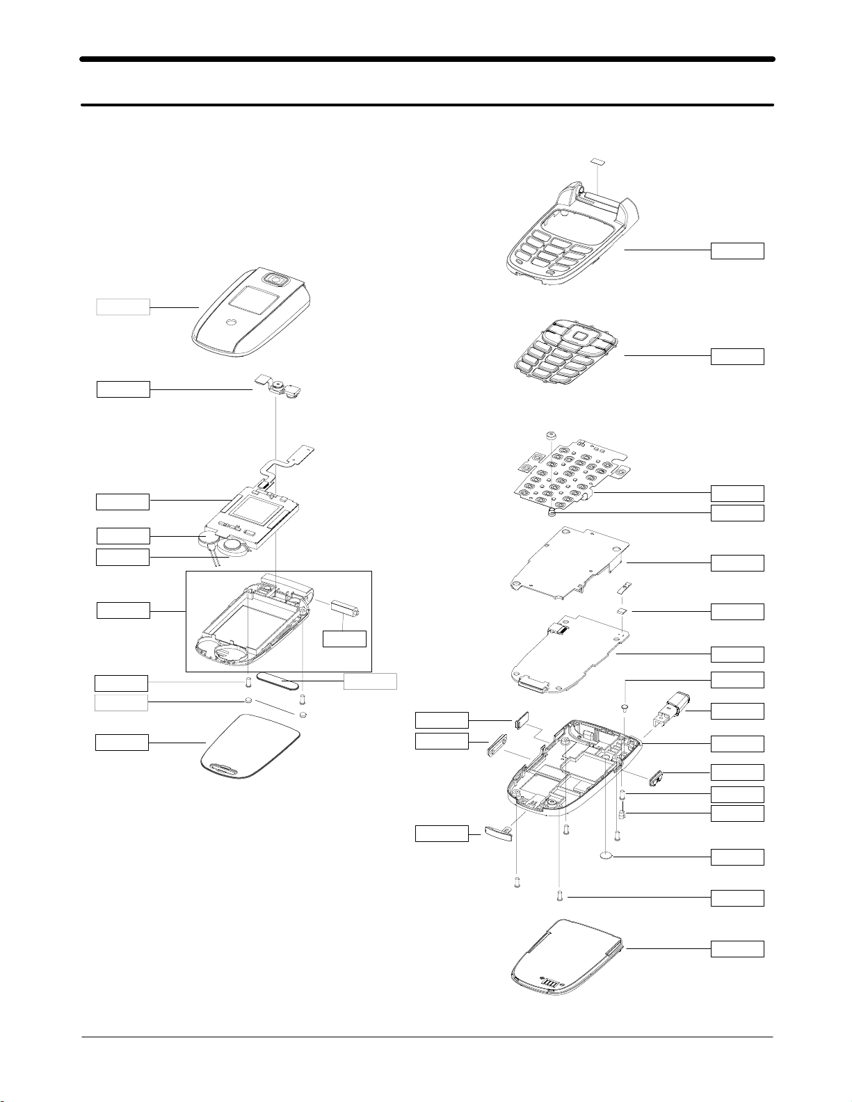
3. Exploded View and Parts List
3-1. Exploded View
QFU01
QCA01
QFR01
QKP01
QLC01
QMO02
QSP01
QFL01
QCR04
QSC12
QMW01
QHI01
QCW01
QRF03
QVO01
QIF01
QME04
QMI01
QSH01
QAN06
QMP01
QCR04
QAN01
QRE01
QCK01
QCR17
QSC13
QRF01
3-1
SAMSUNG Proprietary-Contents may change without notice
This Document can not be used without Samsung's authorization
QCR04
QBA01
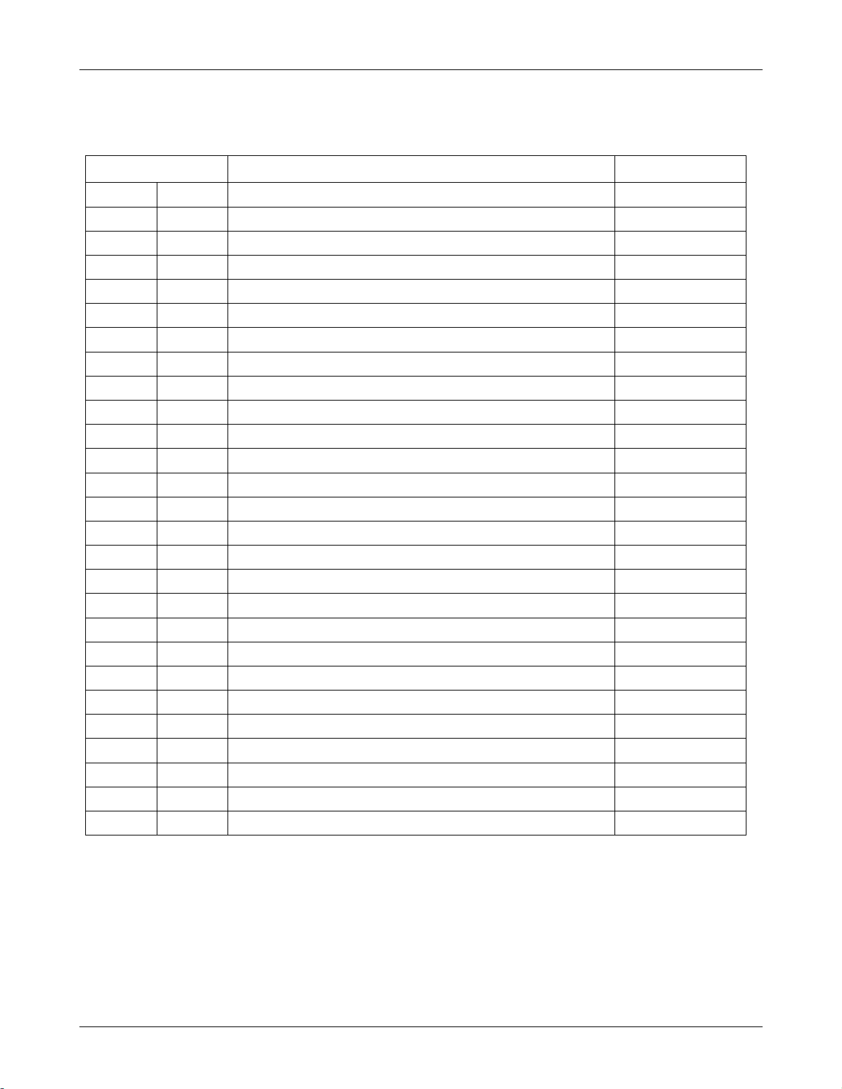
Exploded view and Part List
3-2. Parts List
Location No Description Sec Code
QAN01
QAN06
QBA01
QCA01
QCK01
QCR04
QCR17
QCW01
QFR01
QIF01
QKP01
QLC01
QME04
QMI01
QMO02
QMP01
QMW01
QRE01
QRF01
QRF03
QSC13
QSH01
QSP01
QVO01
QFU01
QFL01
ㅤ
ㅤ
ㅤ
ㅤ
ㅤ
ㅤ
ㅤ
ㅤ
ㅤ
ㅤ
ㅤ
ㅤ
ㅤ
ㅤ
ㅤ
ㅤ
ㅤ
ㅤ
ㅤ
ㅤ
ㅤ
ㅤ
ㅤ
ㅤ
ㅤ
ㅤ
ㅤ
QHI01 MEC-HINGE;SGH-X460,-,-,-,-,-,SIL,- GH75-04948A
ANTENNA-SGHZV10;NSB0402-SS307SVSR,SG GH42-00634A
RMO-RUB ANTENNA CONTACT;SGH-ZV10,CR GH73-05409A
BATTERY-1000M,GRY,EU,M;BST532ABE/STD GH43-02070A
UNIT-CAMERA;SGH-ZV10,IC02044AA,-,EU, GH59-02378A
PMO-KEY CAMERA;SGH-ZV10,ABS+URETHANE GH72-23959A
SCREW-MACHINE;PH,+,-,M1.4,L4,ZPC(BLK 6001-001479
SCREW-MACHINE;PH,+,M1.4,L5,ZPC(BLK), 6001-001645
MEC-CAMERA WINDOW;SGH-ZV10,EU,-,-,-, GH75-07700A
MEC-FRONT COVER;SGH-ZV10,EU,-,-,-,-, GH75-07696A
PMO-IF COVER;SGH-ZV10,PC G31573B+URE GH72-23960A
MEC-KEYPAD;SGH-ZV10,EU,-,-,-,-,BLK,- GH75-07701A
LCD-LCD MODULE;LTD180QC-F0B,SGH-ZV10 GH07-00753A
UNIT-KEY PAD;SGH-ZV10,EDTGZV10K,-,EU GH59-02304A
MICROPHONE-ASSY-6.25MM;2,130~500uA,- GH30-00177F
MOTOR-DC;12000rpm,0g.cm,3V,90mA 3101-001370
PBA MAIN-SGHZV10 MAIN;SGH-ZV10,VODAF GH92-02376A
MEC-MAIN WINDOW;SGH-ZV10,EU,-,-,-,-, GH75-07699A
MEC-REAR COVER;SGH-ZV10,EU,-,-,-,-,B GH75-07702A
MPR-SHEET RF CAP;SGH-ZV10,PC SHEET,P GH74-16864A
PMO-EAR COVER;SGH-ZV10,PC G31573B,SI GH72-23957A
RMO-REAR SCREW CAP;SGH-ZV10,SI RUBBE GH73-05169A
NDC-SHIELD CAN;-,SGH-ZV10,ZN DIE-CAS GH71-05366A
SPEAKER;0.7W,8ohm,89dB+-2dB,780Hz,18 3001-001823
MEC-KEY VOLUME;SGH-ZV10,EU,-,-,-,-,S GH75-08212A
MEC-FOLDER UPPER;SGH-ZV10,EU,-,-,-,- GH75-07697A
MEC-FOLDER LOWER;SGH-ZV10,EU,-,-,-,- GH75-07698A
3-2
SAMSUNG Proprietary-Contents may change without notice
This Document can not be used without Samsung's authorization
Exploded view and Part List
Description Sec Code
BAG PE;LDPE,T0.05,W80,L180,TRP,-,- 6902-000634
CBF INTERFACE-DATA LINK CABLE;SGH-Z1 GH39-00421A
CHARGER-SGHZ500 TC;TCH137EBE,SGH-Z50 GH44-01007A
S/W CD-PC STUDIO A TYPE;SGH-ZV10,SGH GH46-00172A
UNIT-EARPHONE;SGH-C230,EM-SS550E-STB GH59-02166A
LABEL(P)-WATER SOAK;COMM,NORGE,100G, GH68-02026A
MANUAL-WEEE CARD;COMM,SEC,ENGLISH,UN GH68-07013A
LABEL(R)-MAIN(EU);SGH-ZV10,SAM,POLYE GH68-08100A
MANUAL-USER;SGH-ZV10,VD2,GERMAN,GERM GH68-08158A
MANUAL-QSG;SGH-ZV10,VD2,GERMAN,GERM, GH68-08196A
CUSHION-LOWER CASE;SGH-Z107,PULP,T0. GH69-02401A
BOX(P)-MENUAL BOX(UMTS);SGH-Z107V,SI GH69-02540C
CUSHION-CASE(UP);SGH-ZV10,PULP,T0.8, GH69-03238A
BOX(P)-SGHZV10(UMTS);SGH-ZV10,SC350+ GH69-03251A
PMO-BATTER LOCKER;SGH-ZV10,PC G31573 GH72-23954A
RMO-FOLDER SCREW CAP;SGH-ZV10,SI RUB GH73-05168A
MPR-BOHO VINYL IF;SGH-E720,#950,85X1 GH74-13606A
MPR-PORON MOTOR;SGH-ZV10,SRS,P10XT0. GH74-16844A
MPR-BOHO VINYL WIN/MAIN;SGH-ZV10,ST- GH74-16857A
MPR-BOHO VINYL M/WIN 2;SGH-ZV10,ST-1 GH74-16858A
MPR-BOHO VINYL W/S OUT 3;SGH-ZV10,ST GH74-16865A
MPR-GASKET LCD;SGH-ZV10,CFPWX290,3X2 GH74-17511A
MEC-HANGER;SGH-Z500,TMN,STRAP,-,BLK, GH75-03673H
AS-METAL DOME F/K;SGH-ZV10,METAL DOM GH81-02414A
AS-METAL DOME H/K;SGH-ZV10,METAL DOM GH81-02415A
AS-METAL DOME V/K;SGH-ZV10,METAL DOM GH81-02416A
3-3
SAMSUNG Proprietary-Contents may change without notice
This Document can not be used without Samsung's authorization
Exploded view and Part List
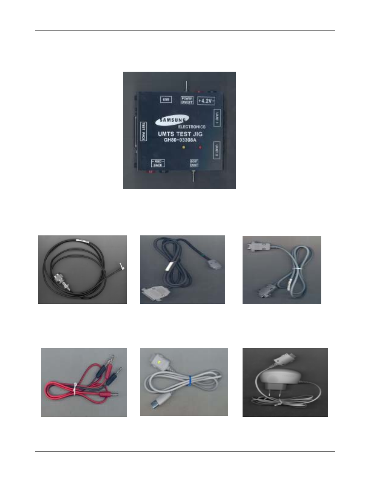
3-3. Test Jig (GH80-03308A)
3-3-1. RF Test Cable
(GH39-00283A)
3-3-2. Test Cable
(GH39-00337E)
3-3-4. Power Supply Cable 3-3-5. DATA CABLE
(GH39-00279A)
3-3-3. Serial Cable
3-3-6. TC
(GH44-00701A)
3-4
SAMSUNG Proprietary-Contents may change without notice
This Document can not be used without Samsung's authorization
4. Electrical Parts List
SEC CODE Description Design LOC
AN101 COMP-SMD 4202-001048
BAT500 BATTERY 4302-001177
C100,C103,C118,C127 C-CERAMIC,CHIP 2203-000254
C101,C104,C108,C109 C-CERAMIC,CHIP 2203-000812
C102,C116,C141,C151 C-CERAMIC,CHIP 2203-000438
C105,C110,C112,C115 C-CERAMIC,CHIP 2203-005482
C111,C117,C122,C126 C-CERAMIC,CHIP 2203-000812
C113,C203,C244 C-CERAMIC,CHIP 2203-000885
C114,C123,C129,C610 C-CERAMIC,CHIP 2203-000854
C119,C200,C206,C217 C-CERAMIC,CHIP 2203-000233
C120,C124,C144,C238 C-CERAMIC,CHIP 2203-000995
C121,C128,C138,C139 C-CERAMIC,CHIP 2203-005482
C125,C222,C225 C-CERAMIC,CHIP 2203-005288
C130 C-CERAMIC,CHIP 2203-000725
C132,C137,C140,C146 C-CERAMIC,CHIP 2203-000812
C133 C-CERAMIC,CHIP 2203-000836
C134,C142,C215,C216 C-CERAMIC,CHIP 2203-002668
C145,C426 C-CERAMIC,CHIP 2203-006141
C147,C229,C505,C517 C-CERAMIC,CHIP 2203-006208
C148,C201,C218,C220 C-CERAMIC,CHIP 2203-005482
C149,C150,C156,C168 C-CERAMIC,CHIP 2203-000254
C152 C-CERAMIC,CHIP 2203-000311
C153,TA720 C-TA,CHIP 2404-001274
C154,C341 C-CERAMIC,CHIP 2203-005480
C159,C210,C248,C340 C-CERAMIC,CHIP 2203-000812
C160 C-CERAMIC,CHIP 2203-005503
C161 C-CERAMIC,CHIP 2203-002443
C162 C-CERAMIC,CHIP 2203-005234
C163,C165,C617,C644 C-CERAMIC,CHIP 2203-000386
C169,C235,C239,C337 C-CERAMIC,CHIP 2203-000254
TA204,C236,TA411 C-TA,CHIP 2404-001225
C205,C207,C211 C-CERAMIC,CHIP 2203-000330
C208,C209,C645,C646 C-CERAMIC,CHIP 2203-000278
C221,C227,C231,C234 C-CERAMIC,CHIP 2203-000233
C224,C226,C230,C233 C-CERAMIC,CHIP 2203-005482
C228,C242 C-CERAMIC,CHIP 2203-000679
C237,C406 C-CERAMIC,CHIP 2203-006257
C240,C424,C428,C540 C-CERAMIC,CHIP 2203-005482
C241,C421,C689,C697 C-CERAMIC,CHIP 2203-000438
C243 C-CERAMIC,CHIP 2203-000940
C247,C339,C423 C-CERAMIC,CHIP 2203-000233
C300,C320,C330,C353 C-CERAMIC,CHIP 2203-006093
C301,C302,C303,C304 C-CERAMIC,CHIP 2203-006194
C305,C308,C309,C404 C-CERAMIC,CHIP 2203-005806
C306,C307,C331,C332 C-CERAMIC,CHIP 2203-006194
C310,C311,C312,C313 C-CERAMIC,CHIP 2203-006423
C314,C315,C316,C317 C-CERAMIC,CHIP 2203-006423
C318,C319,C321,C322 C-CERAMIC,CHIP 2203-006423
C323,C324,C325,C326 C-CERAMIC,CHIP 2203-006423
C327,C328,C329,C343 C-CERAMIC,CHIP 2203-006423
4-1
SAMSUNG Proprietary-Contents may change without notice
This Document can not be used without Samsung's authorization

Electrical Parts List
SEC CODE Description Design LOC
C333,C403,C414 C-CERAMIC,CHIP 2203-006194
C334,C335 C-CERAMIC,CHIP 2203-000628
C336 C-CERAMIC,CHIP 2203-000489
C338,C342,C420,C422 C-CERAMIC,CHIP 2203-000254
C346,C348,C350,C352 C-CERAMIC,CHIP 2203-006423
C347,C351 C-CERAMIC,CHIP 2203-006091
C354,C520,C524,C527 C-CERAMIC,CHIP 2203-006201
C355,C400,C401,C402 C-CERAMIC,CHIP 2203-006423
C409,C410,C417,C427 C-CERAMIC,CHIP 2203-006324
C412,C413,C416,C419 C-CERAMIC,CHIP 2203-006423
C415,C536,C537,C541 C-CERAMIC,CHIP 2203-005806
C418 C-CERAMIC,CHIP 2203-006053
TA425 C-TA,CHIP 2404-001394
C429 C-TA,CHIP 2404-001386
C500,C501 C-CERAMIC,CHIP 2203-005138
C502,C506,C511,C514 C-CERAMIC,CHIP 2203-006423
C508,C516,C530,C532 C-CERAMIC,CHIP 2203-006093
C509 C-CERAMIC,CHIP 2203-005736
C515,C549,C550,C551 C-CERAMIC,CHIP 2203-006423
C518,C522,C523,C546 C-CERAMIC,CHIP 2203-006208
C521,C526,C529,C531 C-CERAMIC,CHIP 2203-006344
C528,C577 C-CERAMIC,CHIP 2203-006201
C533 C-CERAMIC,CHIP 2203-006344
C538,C539,C544,C703 C-CERAMIC,CHIP 2203-000812
C542,C543,C672 C-CERAMIC,CHIP 2203-005806
TA545 C-TA,CHIP 2404-001281
C547,C548,C657,C673 C-CERAMIC,CHIP 2203-006208
C552,C553,C554,C562 C-CERAMIC,CHIP 2203-006423
C563,C628,C658,C674 C-CERAMIC,CHIP 2203-006423
C572 C-CERAMIC,CHIP 2203-006324
C573,C574 C-CERAMIC,CHIP 2203-000425
C578,C602,C603,C604 C-CERAMIC,CHIP 2203-006093
C606,C608,C688,C725 C-CERAMIC,CHIP 2203-006093
TA607,TA615,TA690,TA691 C-TA,CHIP 2404-001348
C616,C635,C639,C643 C-CERAMIC,CHIP 2203-003054
C621,C625,C626,C629 C-CERAMIC,CHIP 2203-000854
TA624,TA726 C-TA,CHIP 2404-001381
C630,C633,C650,C651 C-CERAMIC,CHIP 2203-000854
C637,C638,C647,C648 C-CERAMIC,CHIP 2203-006137
TA641,TA642 C-TA,CHIP 2404-001352
C655,C656,C665,C666 C-CERAMIC,CHIP 2203-000854
C662,C671 C-CERAMIC,CHIP 2203-006190
C667,C687,C730,C731 C-CERAMIC,CHIP 2203-000854
C675,C686,C694,C696 C-CERAMIC,CHIP 2203-006423
C692 C-CERAMIC,CHIP 2203-006137
TA693,TA750,TA751 C-TA,CHIP 2404-001339
C695 C-CERAMIC,CHIP 2203-000654
C698,C699 C-CERAMIC,CHIP 2203-005481
C702 C-CERAMIC,CHIP 2203-006399
C704,C706,C707 C-CERAMIC,CHIP 2203-005482
4-2
SAMSUNG Proprietary-Contents may change without notice
This Document can not be used without Samsung's authorization

Electrical Parts List
SEC CODE Description Design LOC
C721 C-CERAMIC,CHIP 2203-006556
C729 C-CERAMIC,CHIP 2203-000812
C733 C-CERAMIC,CHIP 2203-006423
C736 C-CERAMIC,CHIP 2203-000386
ANT100 CONNECTOR-COAXIAL 3705-001358
SIM500 CONNECTOR-CARD EDGE 3709-001355
EAR600 JACK-PHONE 3722-002175
CN701 CONNECTOR-HEADER 3711-005777
CN704 CONNECTOR-HEADER 3711-005296
IFC705 CONNECTOR-SOCKET 3710-002120
BTC706 CONNECTOR-HEADER 3711-005829
D501 DIODE-ARRAY 0407-001002
F100 FILTER-SAW 2904-001550
F101 FILTER-SAW 2904-001570
F102 FILTER-SAW 2904-001571
F200 FILTER-SAW 2904-001439
F201 FILTER-SAW 2904-001438
F203 FILTER 2910-000004
F204,F621,F622,F623 FILTER-EMI SMD 2901-001326
L101,R131,R213,R214 R-CHIP 2007-000171
L102,L108,L112,L113 INDUCTOR-SMD 2703-002203
L103,L125,L126,L200 INDUCTOR-SMD 2703-002314
L105 INDUCTOR-SMD 2703-001723
L107,L109 INDUCTOR-SMD 2703-002208
L110,L400,L600,L701 CORE-FERRITE BEAD 3301-001534
L111,L114,L115,L117 INDUCTOR-SMD 2703-001229
L116,L119,L121,L123 INDUCTOR-SMD 2703-002176
L118,L204 INDUCTOR-SMD 2703-002268
L120 INDUCTOR-SMD 2703-002199
L128 INDUCTOR-SMD 2703-002369
L129 INDUCTOR-SMD 2703-002203
L130 INDUCTOR-SMD 2703-001178
L201 INDUCTOR-SMD 2703-002198
L202 INDUCTOR-SMD 2703-002205
L203 INDUCTOR-SMD 2703-002267
L205 INDUCTOR-SMD 2703-001750
L206,L209,L210 CORE-FERRITE BEAD 3301-001729
L207,L208,L211 INDUCTOR-SMD 2703-002368
L501,L502 INDUCTOR-SMD 2703-002653
L601,L602 CORE-FERRITE BEAD 3301-001630
L703,L706,L707 CORE-FERRITE BEAD 3301-001534
L708 CORE-FERRITE BEAD 3301-001756
IRD400 PHOTO-IRDA 0604-001261
MIS201 RF-MODULE 4709-001370
VCO101 OSCILLATOR-VCO 2806-001360
TCX200 OSCILLATOR-VCTCXO 2809-001280
VCO201 COMP-SMD 2806-001367
OSC501 CRYSTAL-UNIT 2801-004373
R100 R-CHIP 2007-007491
R101,R126,R127,R130 R-CHIP 2007-000138
4-3
SAMSUNG Proprietary-Contents may change without notice
This Document can not be used without Samsung's authorization
Electrical Parts List
SEC CODE Description Design LOC
R102,R312 R-CHIP 2007-000140
R105,R108,R110,R203 R-CHIP 2007-007318
R106,R112,R212 R-CHIP 2007-000172
R107,R633 R-CHIP 2007-007316
R111 R-CHIP 2007-000145
R114,R128,R129 R-CHIP 2007-001217
R115,R116 R-CHIP 2007-001291
R117,R123 R-CHIP 2007-001301
R118,R119,R120,R121 R-CHIP 2007-001307
R122 R-CHIP 2007-003112
R124 R-CHIP 2007-000147
R125,R330 R-CHIP 2007-007142
R200 R-CHIP 2007-008137
R201 R-CHIP 2007-000173
R202,R210,R211 R-CHIP 2007-000138
R204 R-CHIP 2007-000141
R206,R208,R315 R-CHIP 2007-007314
R209,R505 R-CHIP 2007-001298
R216 R-CHIP 2007-007001
R217 R-CHIP 2007-000146
R303,R405,R507,R510 R-CHIP 2007-000171
R307,R309,R344,R424 R-CHIP 2007-008542
R310 R-CHIP 2007-007135
R313 R-CHIP 2007-000137
R314,R602,R603,R614 R-CHIP 2007-007318
R327,R332,R720,R723 R-CHIP 2007-000148
R328,R331,R620 R-CHIP 2007-001339
R339,R650 R-CHIP 2007-000566
R341,R342 R-CHIP 2007-008588
R345,R346,R347,R348 R-CHIP 2007-007014
R349 R-CHIP 2007-007014
R403,R419 R-CHIP 2007-000162
R410,R503 R-CHIP 2007-008516
R411,R700 R-CHIP 2007-008055
R413,R511,R617 R-CHIP 2007-007107
R415 R-CHIP 2007-001313
R418 R-CHIP 2007-007141
R420,R421,R422,R423 R-CHIP 2007-001305
R500,R501 R-CHIP 2007-003015
R504 R-CHIP 2007-008483
R506 R-CHIP 2007-007468
R508 R-CHIP 2007-000151
R514,R634,R711,R712 R-CHIP 2007-000171
R519 R-CHIP 2007-007139
R604,R605,R610,R612 R-CHIP 2007-007137
R615 R-CHIP 2007-007318
R616,R618 R-CHIP 2007-007334
R623,R625 R-CHIP 2007-007311
R643 R-CHIP 2007-000159
R644,R645 R-CHIP 2007-000775
4-4
SAMSUNG Proprietary-Contents may change without notice
This Document can not be used without Samsung's authorization
 Loading...