

Samsung ZM60 Service Manual
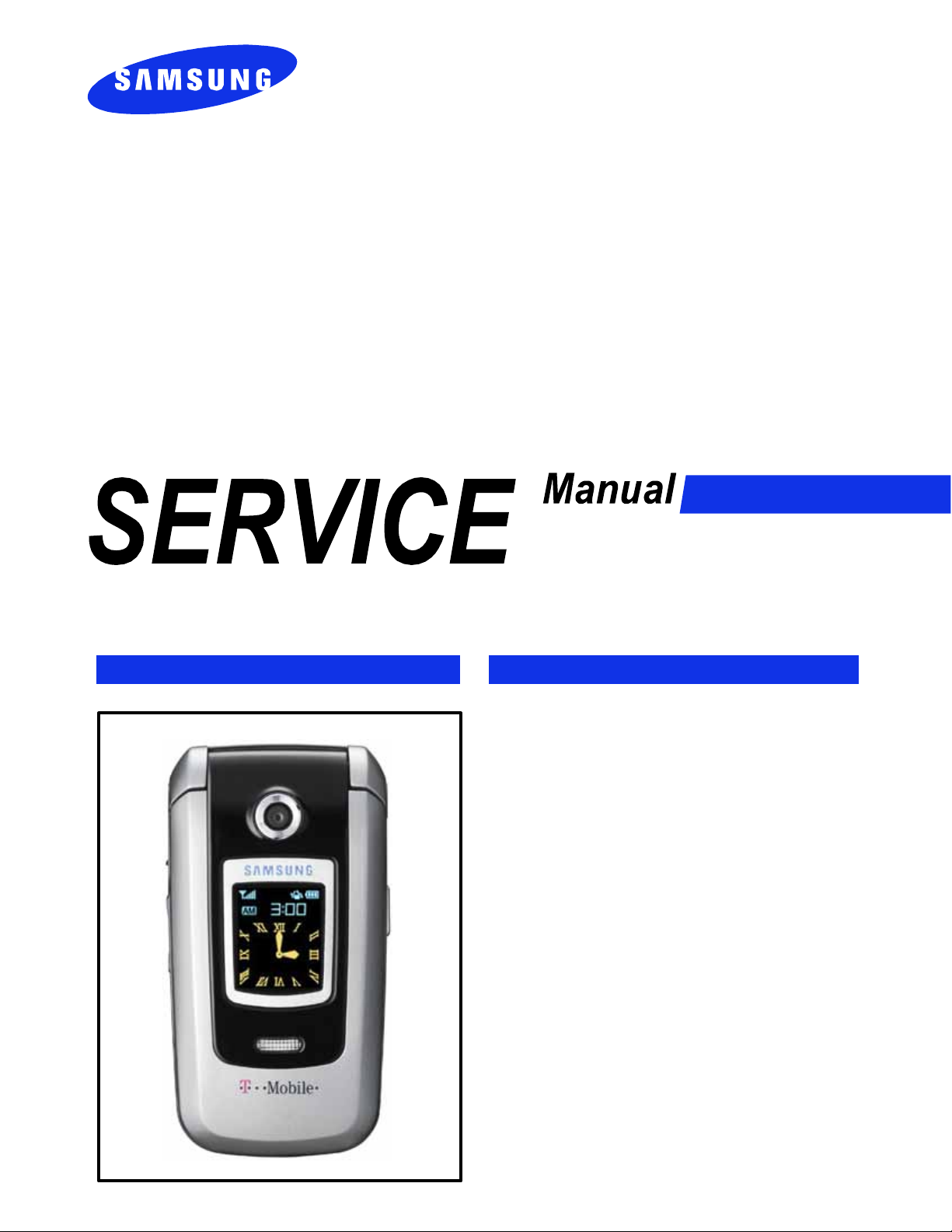
UMTS TELEPHONE
SGH-ZM60
UMTS TELEPHONE
CONTENTS
1. Specification
2. Circuit Description
3. Exploded Views and Parts List
4. Electrical Parts List
5. Block Diagrams
6. PCB Diagrams
7. Flow Chart of Troubleshooting

This Service Manual is a property of Samsung Electronics Co.,Ltd.
Any unauthorized use of Manual can be punished under applicable
International and/or domestic law.
ⓒ
Samsung Electronics Co.,Ltd. June. 2005
Printed in Korea.
Code No.: GH68-07575A
BASIC.
1. Specification
1-1. GSM General Specification
EGSM 900 DCS1800 PCS1900 W-CDMA
Freq.
Band[MHz]
Uplink/Downlink
ARFCN range
Tx/Rx spacing 45MHz 95MHz 80MHz 190MHz
Mod. Bit rate/
Bit Period
Time Slot
Period/Frame
Period
Modulation 0.3GMSK 0.3GMSK 0.3GMSK
MS Power 33dBm~5dBm 30dBm~0dBm 30dBm~0dBm 24dBm ~ - 50dBm
Power Class
880~915
925~960
0~124 &
975~1023
270.833kbps
3.692us
576.9us
4.615ms
4
(max +33dBm)1(max +30dBm)1(max +30dBm)
1710~1785
1805~1880
512~885 512~810
270.833kbps
3.692us
576.9us
4.615ms
1850~1910
1930~1990
270.833kbps
3.692us
576.9us
4.615ms
1920~1980
2110~2170
UL:9612~9888
DL:10562~10838
3.84Mcps
Frame length : 10ms
Slot length : 0.667ms
QPSK
HQPSK
3
(max +24dBm)
Sensitivity -102dBm -100dBm -100dBm -106.7dBm
TDMA Mux 8 8 8
Cell Radius 35Km 2Km 2Km 2Km
1-1
SAMSUNG Proprietary-Contents may change without notice
This Document can not be used without Samsung's authorization
Specification
1-2. GSM TX power class
TX Power
control level
5 33±2 dBm
6 31±2 dBm
7 29±2 dBm
8 27±2 dBm
9 25±2 dBm
10 23±2 dBm
11 21±2 dBm
GSM900
TX Power
control level
0 30±3 dBm
1 28±3 dBm
2 26±3 dBm
3 24±3 dBm
4 22±3 dBm
5 20±3 dBm
6 18±3 dBm
DCS1800
TX Power
control level
0 30±3 dBm
1 28±3 dBm
2 26±3 dBm
3 24±3 dBm
4 22±3 dBm
5 20±3 dBm
6 18±3 dBm
PCS1900
12 19±2 dBm
13 17±2 dBm
14 15±2 dBm
15 13±2 dBm
16 11±3 dBm
17 9±3dBm
18 7±3 dBm
19 5±3 dBm
7 16±3 dBm
8 14±3 dBm
9 12±4 dBm
10 10±4 dBm
11 8±4dBm
12 6±4 dBm
13 4±4 dBm
14 2±5 dBm
7 16±3 dBm
8 14±3 dBm
9 12±4 dBm
10 10±4 dBm
11 8±4dBm
12 6±4 dBm
13 4±4 dBm
14 2±5 dBm
15 0±5 dBm
1-2
15 0±5 dBm
SAMSUNG Proprietary-Contents may change without notice
This Document can not be used without Samsung's authorization

2. Circuit Description
2-1. SGH-ZM60 RF Circuit Description
- Antenna Switch Module (U600)
The antenna switch module allows multiple operating bands and modes to share the same antenna. A common
antenna connects to one of five paths: 1) UMTS-2100 Rx/Tx, 2) EGSM-900 Rx, 3) EGSM-900 Tx, 4) DCS-1800
Rx, and 5) DCS-1800 Tx. 6) PCS-1900 Tx, 7) PCS-1900 Rx, UMTS operation requires simultaneous reception
and transmission.
-Filter
To convert Electromagnetic Field Wave to Acoustic Wave and then pass the specific frequency band.
- GSM Rx FILTER (F601)→For filtering the frequency band between 925 ~ 960 MHz.
- DCS Rx FILTER (F602)→For filtering the frequency band 1805 and 1880 MHz.
- DCS Rx FILTER (F603)→For filtering the frequency band 1930 and 1990 MHz.
- WCDMA Rx FILTER (F701)→For filtering the frequency band 2110 and 2170 MHz.
- WCDMA Tx FILTER (F703)→For filtering the frequency band 1920 and 1980 MHz.
- VCTCXO (OSC701)
To generate the 19.2MHz reference clock to drive the logic and RF.
- Duplexer (F202)
A duplexer splits a single operating band into receive and transmit paths.
- UMTS PAM (U701)
This is a key component in the transmitter chain and must complement the RTR6250 IC precisely; jointly they
dominate the UMTS transmitter performance characteristics. Parameters such as gain, output power level, ACLR,
harmonics, Rx-band noise, and power supply current are critical.
- GSM/DCS/PCS PAM (U603)
The PAM is a key component in any transmitter chain and must complement the rest of the transmitter precisely.
For GSM,DCS,PCS operation, the closed-loop transmit power control functions add even more requirements
relative to the UMTS PA. In addition to gain control and switching requirements, the usual RF parameters such
as gain, output power level, several output spectrum requirements, and power supply current are critical.
- GSM/DCS/PCS l Tx VCO (U601)
The Tx VCO outputs for EGSM, DCS, PCS drive a resistive network that splits the active signal into two signals:
1) the input to the active PAM – this is the low loss path, and 2) the OPLL feedback signal.
- RF VCO (OSC702)
The single-band UHF VCO is a key component within its phase-locked loop; VCO performance directly impacts
PLL and transceiver performance. UMTS Rx LO signal is generated from this VCO's output.
2-1
SAMSUNG Proprietary-Contents may change without notice
This Document can not be used without Samsung's authorization

Circuit Description
- RFL6200 (U702)
The RFL6200 includes an LNA circuit optimized for UMTS-2100 operation. The LNA is separated from all other
receive functions contained within the RFR6200 receiver IC to improve mixer LO to RF isolation – a critical
parameter in the Zero-IF architecture.
- RFR6200 (U703)
The RFR6200 provides the Zero-IF receiver signal path, from RF to analog baseband, for UMTS-2100
applications. The RFR6200 accepts its UMTS input signal from the handset RF front-end design. The UMTS input
is configured differentially to optimize second-order inter-modulation and common mode rejection performance, and
implements MSM-controlled gain adjustments to extend the receiver dynamic range.
- RTR6250 (U602)
The RTR6250 supports multi-band, multi-mode phones with two receiver signal paths and three transmitter signal
paths:
Receiver paths
- EGSM-900
-DCS-1800
- PCS-1900
Transmitter paths
- EGSM-900 (using OPLL technique)
- DCS-1800 (using OPLL technique)
- PCS-1900
- UMTS-2100
Numerous secondary functions are integrated on-chip as well:
2-2
SAMSUNG Proprietary-Contents may change without notice
This Document can not be used without Samsung's authorization

Circuit Description
2-2. Baseband Circuit description of SGH-ZM60
2-2-1. PM6650
- Power Management
Ten low-dropout regulators designed specifically for GSM applications power the terminal and help ensure optimal
system performance and long battery life. It provides LDOs support for 1.375V, 1.8V, 2.6V, 2.85V,
3.3V.
IC-level interfaces include the three-line serial bus interface(SBI) used by the MSM6250 device to control
and status the PM6650 IC.
- Keypad Backlight
The Keypad backlight driver output is at pin 23 (KYPD_BACKLIGHT_DRV) and is designed to drive parallel
connected LEDs directly. Its output current level is SBI-programmable and meets the performance specified below.
Input parameters are not specified since they are internal.
- TCXO Controller and Buffers
The PM6650 IC includes circuits for controlling the TCXO warm-up and buffering its signal for distribution
throughout the handset. Performance specifications are presented below.
2-2-2. Connector
- LCD Connector
LCD is consisted of main LCD(color 262K TFT LCD) and small LCD(OLED color 65K LCD). Chip select signals
in the U300, MAIN_LCD_CS can enable main LCD and SUB_LCD_CS can enable small LCD. CAM_PWR_ON
signal enables white LED of main LCD. MAIN_LCD_RESET signal initiates the reset
process of the main LCD. SUB_LCD_RESET signal initiates the Reset process of the small LCD.
16-bit data lines(D2(0)~D(15)) transfers data and commands to LCD. Data and commands use "RS" signal.
If this signal is high, Inputs to LCD are commands. If it is low, Inputs to LCD are data. The signal which informs
the input or output state to LCD, is required. But this system is not necessary this signal.
Power signals for LCD are "VBATT_LCD". "SPKP_RCVP" and "SPKP_RCVN" from HEA401 are used for audio
speaker. And "MOTOR_EN" from U100 enables the motor.
-Key
This is consisted of key interface pins among U100, KEYSENSE_N(0:4). These signals compose the matrix.
Result of matrix informs the key status to key interface in the U100. Power on/off key is seperated from the
matrix. The key LED use the "VBATT" supply voltage. "KEY_LED" signal enables LEDs with current control.
"HALL_SW" informs the status of folder (open or closed) to the. This uses the hall effect IC, A3212ELH.
2-3
SAMSUNG Proprietary-Contents may change without notice
This Document can not be used without Samsung's authorization

Circuit Description
- EMI ESD Filter
This system uses the EMI ESD filter, GMF05LC to protect noise from IF CONNECTOR part.
- IF connetor
It is 24-pin connector. They are designed to use VBATT, CF, UART1_TX, UART1_RX, UART1_RFR,
UART1_CTS, JIG_ON, RTCK, TCK, TDI, TDO, TMS and GND. They connected to power supply IC,
microprocessor and signal processor IC.
2-2-3. Audio
EAR1OP and EAR1ON from U100 are connected to the main speaker. AUXOP and AUXON are connected to
the Digital AMP. MIC1P and MIC1N are connected to the main MIC. And MIC2P and MIC2N are connected to
the Earphone.
YMU769 has a built-in amplifier, and thus, is an ideal device for outputting sounds that are used by mobile
phones in addition to game sounds and ringing melodies that are replayed by a synthesizer.
The synthesizer section adopts "stereophonic hybrid synthesizer system" that are given advantages of both FM
synthesizers and Wave Table synthesizers to allow simultaneous generation of up to 32 FM voices and 32 Wave
Table voices. Furthermore, YMU769 has a built-in hardware sequencer that helps to realize complex play without
heavily loading the host CPU. And this device also has a built-in circuit for controlling vibrators and LEDs
synchronizing with play of music. The consumed electric current can be stopped to the minimum by power down
mode when not operating.
The hardware sequence built in this device allows playing of the complex music without giving excessive load to
the CPU of the portable telephones. Moreover, the registers of the FM synthesizer can be operated directly for
real time sound generation, allowing, for example, utilization of various sound effects when using the game
software installed in the portable telephone.
2-2-4. Memory
The signals in the MSM6250 enable two memories. They use only one volt supply voltage, VDD_LP from
the PM6650. This system uses SEC's memory, KBE00F005M-F411. It is consisted of 1G bits flash NAND
memory and 512M bits SDRAM memory. It has 16 bit data line, D1[0~15] which is connected to MSM6250.
It has 22 bit address lines, A[1~22]. ROM_CS and RAM_CS signals is chip select.
2-2-5. Camera
The camera module consists of Mega pixel and VGA pixel. The Mega camera is a highly integrated CMOS color
image sensor implemented by Hynix COMS sensor process realizing high sensitivity and wide dynamic range.
Total pixel array size is 1184H x 914V, and 1170H x 880V pixels are active. The VGA camera is a
highly integrated CMOS color image sensor implemented by Hynix COMS sensor process realizing high sensitivity
and wide dynamic range. Total pixel array size is 656H x 492V, and 656H x 488V pixels are active.
2-2-6. Irda
This system uses IRDA module, HSDL_3208, Agilent's. This has signals, "IRA_DOWN"(enagle signal),
"RXD0"(Input data) and "TXD0"(output data). These signals are connected to U100(MSN6250). It uses two power
signals. "VDD_LP" is used for circuit and "VBATT" is used for LED.
2-4
SAMSUNG Proprietary-Contents may change without notice
This Document can not be used without Samsung's authorization
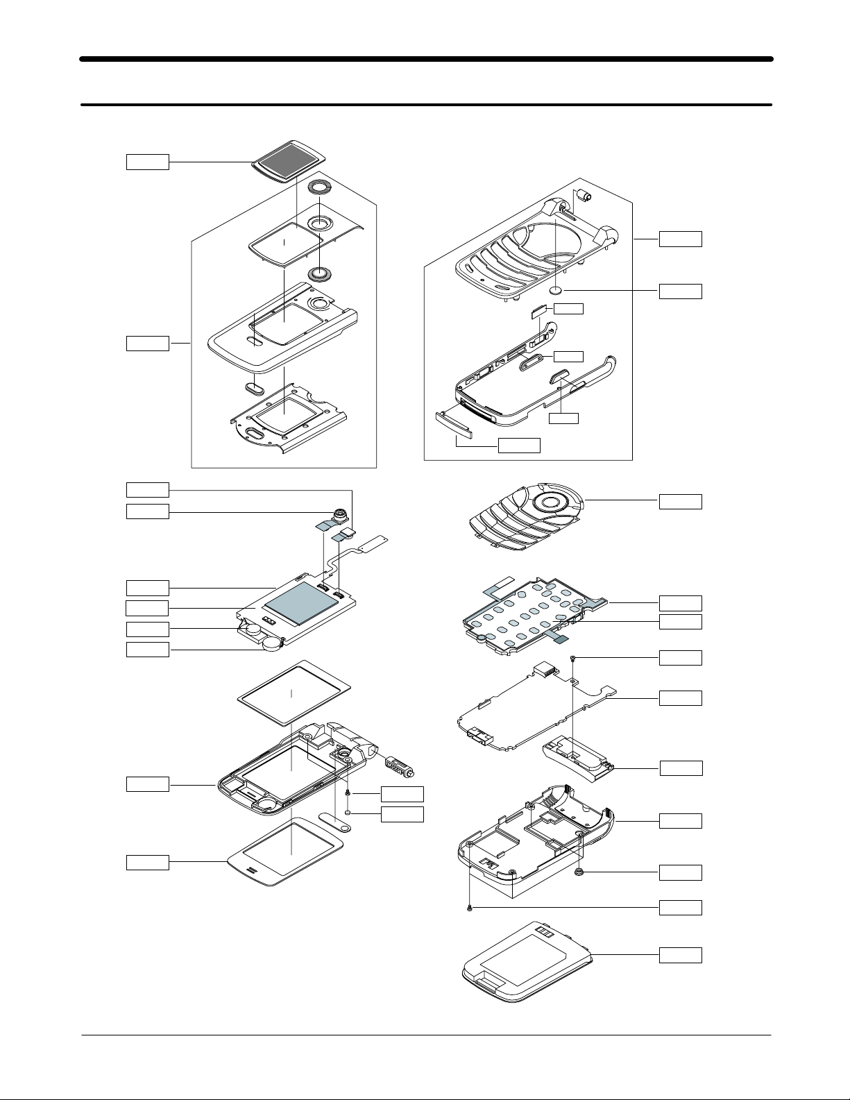
3. Exploded View and Parts List
3-1. Exploded View
QWD03
QFR01
QSC14
QRF03
QFU01
QCA03
QCA01
QLC01
QLC02
QAU01
QMO01
QVO01
QCK01
QIF01
QKP01
QSH01
QME01
QCR06
QMP01
QFL01
QMW01
QCR04
QSC01
3-1
SAMSUNG Proprietary-Contents may change without notice
This Document can not be used without Samsung's authorization
QAN02
QRE01
QRF01
QCR09
QBA01
Exploded view and Part List
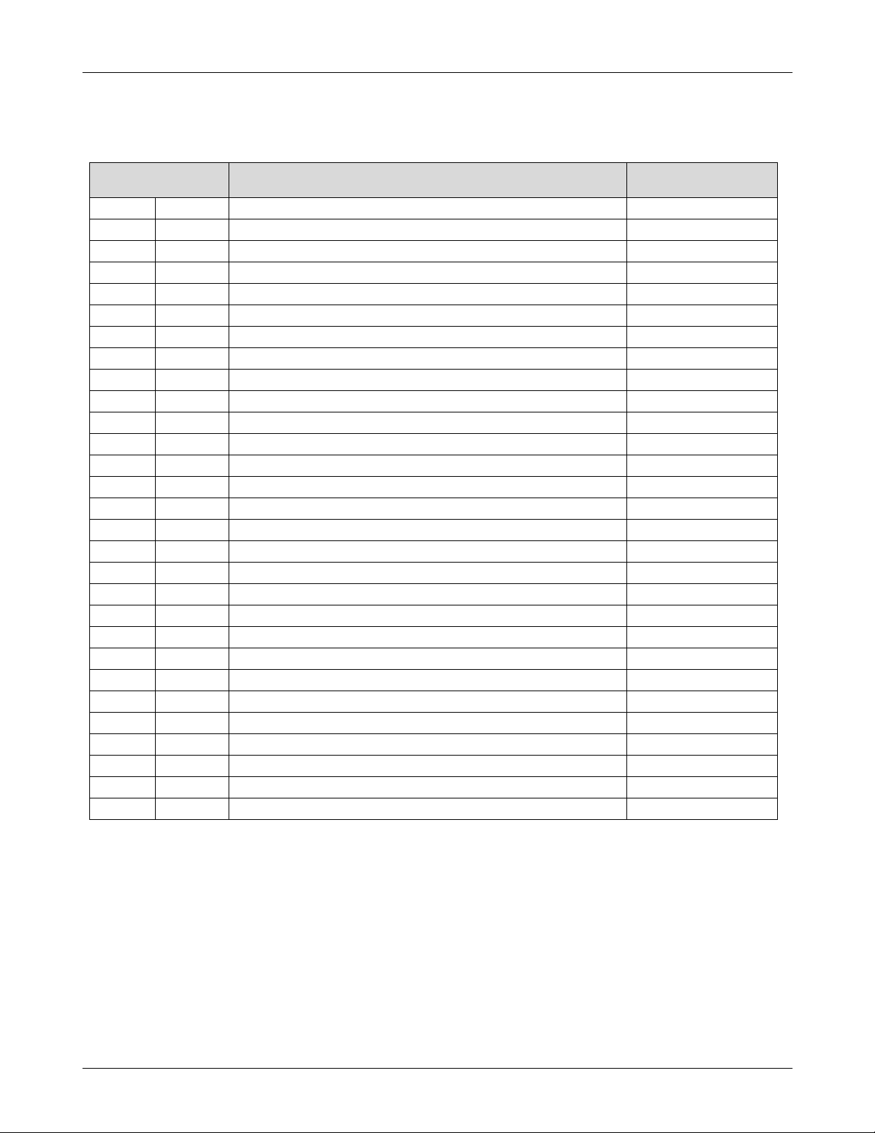
3-2. Parts List
Location NO. Description SEC CODE
QAU01
QCR06
QCR04
QCR09
QLC01
QLC02
QMO01
QMO01
QAN02
QBA01
QCA01
QCA03
QME01
QSH01
QSC01
QRF01
QSC14
QFR01
QFL01
QRE01
QWD03
QFU01
QKP01
QMW01
QMP01
ㅤ
ㅤ
ㅤ
ㅤ
ㅤ
ㅤ
ㅤ
ㅤ
ㅤ
ㅤ
ㅤ
ㅤ
ㅤ
ㅤ
ㅤ
ㅤ
ㅤ
ㅤ
QVO01 PMO-KEY VOL;SGH-Z300,ABS+URETHANE,SI GH72-19860A
QCK01 PMO-KEY CAM;SGH-Z300,ABS+URETHANE,SI GH72-19861A
ㅤ
QIF01 PMO-IF COVER;SGH-Z300,PC+URETHANE,BK GH72-19863A
ㅤ
QRF03 PMO-COVER EAR;SGH-Z300,PC+URETHANE,B GH72-22285A
ㅤ
ㅤ
ㅤ
ㅤ
ㅤ
ㅤ
ㅤ
AUDIO-RECEIVER;32ohm,110dB,8X16mm 3009-001111
SCREW-MACHINE;PH(PI2.5),+,M1.4,L3.5, 6001-001155
SCREW-MACHINE;PH,+,M1.4,L4,NYLOK,SWR 6001-001479
SCREW-MACHINE;PH,+,M1.4,L4.5,ZPC(BLK 6001-001670
LCD;LTS200QC-F0C,SGH-Z300,176X220,31 GH07-00735A
LCD-SGHZ300 SUB MODULE;PM08CC021A,SG GH07-00742A
MOTOR DC-SGHZ130;DMJBRK20BB,SGH-Z130 GH31-00153K
MOTOR DC-SGHZ130;DMJBRK20BB,SGH-Z130 GH31-00153K
INTENNA-SGHZ300;H90-OY354,SGH-Z300,8 GH42-00563A
BATTERY-BATTERY-960MAH,DA SI;BST4309 GH43-01789A
UNIT-CAMERA;SGH-Z300,MOMFA140U1A,-,E GH59-02027A
UNIT-CAMERA;SGH-Z300,MOMFA240U1A,-,E GH59-02028A
UNIT-KEY PAD;SGH-Z300,EDTGZ300,-,EU, GH59-02044A
NDC-SHIELD CAN;-,SGH-Z300,MAGNESIUM, GH71-04748A
MPR-SCREW CAP;SGH-Z300,0.3T PC SHEET GH74-14084A
MPR-RF CAP;SGH-Z300,0.2T PC SHEET,6. GH74-14085A
MPR-TAPE FRONT HOLE;SGH-Z300,PET T0. GH74-15598A
MEC-FRONT COVER;SGH-Z300,EU,-,-,-,-, GH75-06762A
MEC-FOLDER LOWER;SGH-Z300,EU,-,-,-,- GH75-06764A
MEC-REAR COVER;SGH-Z300,EU,-,-,-,-,D GH75-06765A
MEC-DUAL WIN DUMMY;SGH-Z300,EU,-,-,- GH75-06767A
MEC-FOLDER UPPER(TMU);SGH-Z300,TMU,- GH75-07315A
MEC-KEYPAD MAIN(TMU);SGH-Z300,TMU,-, GH75-07319A
MEC-MAIN WIN DUMMY(TMU);SGH-Z300,T-M GH75-07333A
PBA MAIN-SGHZM60;SGH-ZM60,XET,EU,PBA GH92-02201A
3-2
SAMSUNG Proprietary-Contents may change without notice
This Document can not be used without Samsung's authorization
SEC CODE Description
6902-000634 BAG PE;LDPE,T0.05,W80,L180,TRP,-,GH39-00395A CBF INTERFACE-PC DATA CABLE;SGH-Z500
GH44-00701A CHARGER-TCH;TCH137ESE,SGH-X910,AC/DC
GH46-00146A S/W CD-EASY STUDIO TMOBILE;SGH-Z300M
GH59-01713A UNIT-EARPHONE;SGH-Z107,EM-SS650E-ST,
GH68-02026A LABEL(P)-WATER SOAK;SCH-X110,NORGE,1
GH68-07013A MANUAL-WEEE CARD;SGH-E720,SEC,ENGLIS
GH68-07147A MANUAL-USER;SGH-ZM60,T-MOBILE,ENGLIS
GH68-07148A MANUAL-USER;SGH-ZM60,T-MOBILE,GERMAN
GH68-07260A LABEL(R)-MAIN(EU);SGH-ZM60,EU,POLYES
GH69-03038A CUSHION-CASE(1-2);SGH-ZM60,PULP,T0.8
GH69-03039A BOX(P)-UINIT(T-MOBILE);SGH-ZM60,SC30
Exploded view and Part List
GH74-07571A MPR-UPPER LOGO GOHO VINY;SGH-E310,VI
GH74-13606A MPR-BOHO VINYL IF;SGH-E720,#950,85X1
GH74-15543A MPR-SPONGE MIC;SGH-Z300,SRS PORON,81
GH75-03673H MEC-HANGER;SGH-Z500,TMN,STRAP,-,BLK,
3-3
SAMSUNG Proprietary-Contents may change without notice
This Document can not be used without Samsung's authorization

Exploded view and Part List
3-3. Test Jig (GH80-03305A)
3-3-1. RF Test Cable
(GH39-00105A)
3-3-2. Test Cable
(GH39-00210A)
3-3-4. Power Supply Cable 3-3-5. DATA CABLE
(GH39-00208A)
3-3-3. Serial Cable
3-3-6. TC
(GH44-00482A)
3-4
SAMSUNG Proprietary-Contents may change without notice
This Document can not be used without Samsung's authorization
4. Electrical Part List
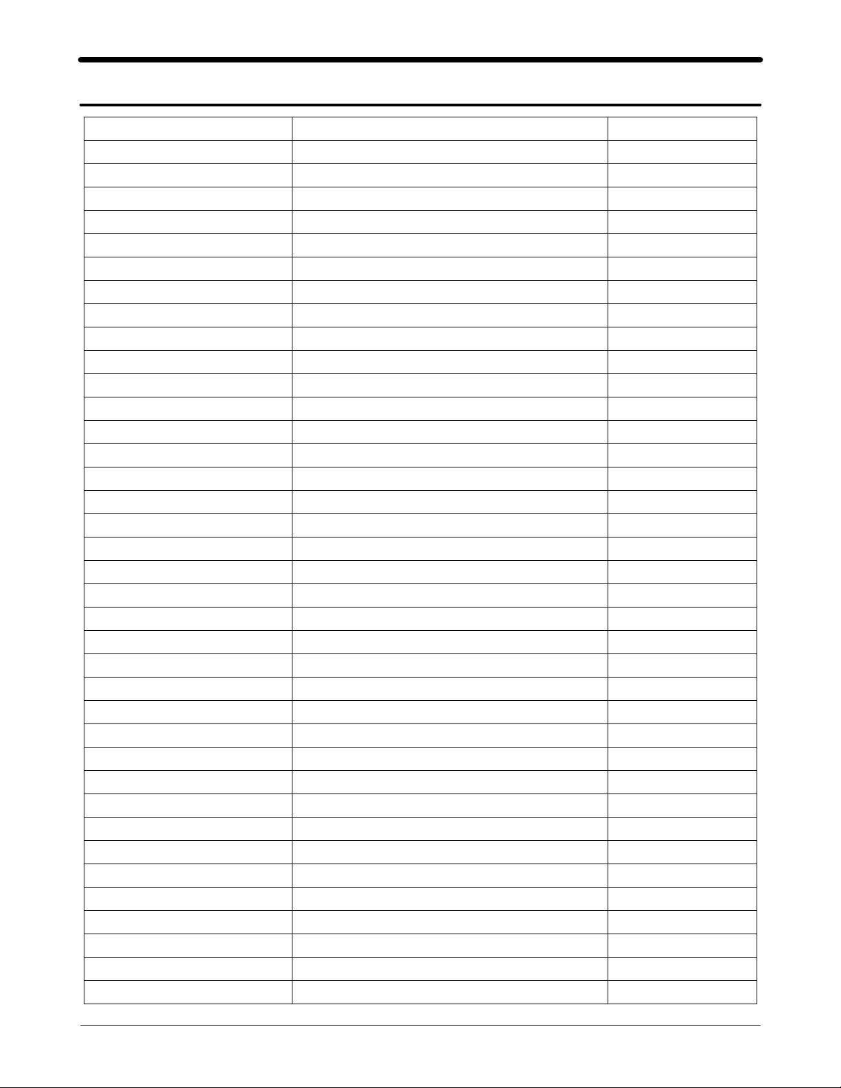
Design LOC Description SEC CODE
ANT601 ANTENNA NEW-ITEM005
BAT201 BATTERY 4302-001180
C101,C102,C103,C104 C-CERAMIC,CHIP 2203-005482
C105,C106,C107,C108 C-CERAMIC,CHIP 2203-005482
C111,C112,C113,C114 C-CERAMIC,CHIP 2203-005482
C115,C117,C119,C120 C-CERAMIC,CHIP 2203-005482
C118,C204,C224,C233 C-CERAMIC,CHIP 2203-006093
C121,C122,C123,C124 C-CERAMIC,CHIP 2203-005482
C125,C126,C127,C128 C-CERAMIC,CHIP 2203-005482
C132,C133,C134,C135 C-CERAMIC,CHIP 2203-005482
C136,C137,C138,C149 C-CERAMIC,CHIP 2203-005482
C141 C-CERAMIC,CHIP 2203-000489
C142,C143 C-CERAMIC,CHIP 2203-000628
C144,C245,C246,C406 C-CERAMIC,CHIP 2203-000812
C145,C148,C250,C254 C-CERAMIC,CHIP 2203-000254
C146,C208,C247,C301 C-CERAMIC,CHIP 2203-005061
C147 C-CERAMIC,CHIP 2203-005480
C151,C153,C154,C156 C-CERAMIC,CHIP 2203-005482
C152,C155 C-CERAMIC,CHIP 2203-006091
C201,C203 C-CERAMIC,CHIP 2203-005138
C202,C214,C216,C217 C-CERAMIC,CHIP 2203-006201
C205,C237,C238,C239 C-CERAMIC,CHIP 2203-005482
C206,C209,C211,C213 C-CERAMIC,CHIP 2203-000278
C207,C226,C228,C316 C-CERAMIC,CHIP 2203-000438
C210 C-CERAMIC,CHIP 2203-005065
C212,C219,C221,C225 C-CERAMIC,CHIP 2203-006208
C215,C220,C502,C504 C-CERAMIC,CHIP 2203-000278
C218,C222,C223,C601 C-CERAMIC,CHIP 2203-006201
C227,C234,C235,C236 C-CERAMIC,CHIP 2203-006208
C229,C230 C-CERAMIC,CHIP 2203-000425
C240,C241,C242,C243 C-CERAMIC,CHIP 2203-005482
C249,C253 C-TA,CHIP 2404-001339
C251,C252,C401,C402 C-CERAMIC,CHIP 2203-006208
C255,C256,C310 C-CERAMIC,CHIP 2203-006053
C302,C303,C307,C308 C-CERAMIC,CHIP 2203-005061
C304,C305,C613,C614 C-CERAMIC,CHIP 2203-000233
C306 C-TA,CHIP 2404-001377
4-1
SAMSUNG Proprietary-Contents may change without notice
This Document can not be used without Samsung's authorization

Electrical Part List
Design LOC Description SEC CODE
C309,C508,C510,C535 C-CERAMIC,CHIP 2203-005061
C311,C313,C315,C405 C-CERAMIC,CHIP 2203-005482
C318,C768 C-CERAMIC,CHIP 2203-000654
C319 C-TA,CHIP 2404-001386
C320 C-CERAMIC,CHIP 2203-006257
C321,C506,C533,C607 C-CERAMIC,CHIP 2203-006093
C327,C413,C769 C-TA,CHIP 2404-001305
C403,C404,C776,C777 C-CERAMIC,CHIP 2203-006208
C407,C411,C412,C627 C-CERAMIC,CHIP 2203-005482
C408,C409,C410,C414 C-CERAMIC,CHIP 2203-000812
C501,C505,C507,C511 C-CERAMIC,CHIP 2203-000854
C503,C514,C523,C538 C-CERAMIC,CHIP 2203-000812
C509,C522,C524,C540 C-CERAMIC,CHIP 2203-000278
C512,C788,C795 C-TA,CHIP 2404-001394
C513,C537 C-CERAMIC,CHIP 2203-005057
C516,C531,C534,C548 C-CERAMIC,CHIP 2203-000854
C520,C521,C545,C546 C-CERAMIC,CHIP 2203-000995
C543,C760,C762,C763 C-CERAMIC,CHIP 2203-005061
C602,C606 C-CERAMIC,CHIP 2203-006201
C603,C626,C632,C637 C-CERAMIC,CHIP 2203-000812
C610,C622,C644,C708 C-CERAMIC,CHIP 2203-000438
C611,C612,C617,C660 C-CERAMIC,CHIP 2203-000854
C615,C616,C621,C701 C-CERAMIC,CHIP 2203-000233
C618 C-CERAMIC,CHIP 2203-001385
C620 C-CERAMIC,CHIP 2203-000885
C623,C625,C635,C650 C-CERAMIC,CHIP 2203-006093
C624 C-CERAMIC,CHIP 2203-000278
C628,C759 C-TA,CHIP 2404-001274
C629,C718 C-CERAMIC,CHIP 2203-000995
C630,C631,C636,C642 C-CERAMIC,CHIP 2203-005482
C633 C-CERAMIC,CHIP 2203-000836
C634 C-TA,CHIP 2301-001512
C638,C739 C-CERAMIC,CHIP 2203-000254
C639 C-CERAMIC,CHIP 2203-000311
C640 C-TA,CHIP 2301-001197
C641 C-CERAMIC,CHIP 2203-000609
C643,C652,C655,C662 C-CERAMIC,CHIP 2203-000812
4-2
SAMSUNG Proprietary-Contents may change without notice
This Document can not be used without Samsung's authorization

Electrical Part List
Design LOC Description SEC CODE
C645 C-CERAMIC,CHIP 2203-005503
C646 C-CERAMIC,CHIP 2203-002443
C647 C-CERAMIC,CHIP 2203-005234
C648,C649,C653,C656 C-CERAMIC,CHIP 2203-005482
C651,C658,C753 C-CERAMIC,CHIP 2203-000386
C654,C661,C665,C761 C-CERAMIC,CHIP 2203-006093
C657,C659,C666,C704 C-CERAMIC,CHIP 2203-005482
C663,C664,C711,C736 C-CERAMIC,CHIP 2203-000812
C667,C668,C669,C670 C-CERAMIC,CHIP 2203-000359
C703,C707,C719,C723 C-CERAMIC,CHIP 2203-000233
C705,C710,C712,C717 C-CERAMIC,CHIP 2203-000330
C709 C-TA,CHIP 2404-001105
C715 C-CERAMIC,CHIP 2203-001383
C720,C724,C726,C730 C-CERAMIC,CHIP 2203-005482
C725,C727,C732,C735 C-CERAMIC,CHIP 2203-000233
C728,C733 C-CERAMIC,CHIP 2203-005288
C729,C749 C-CERAMIC,CHIP 2203-000438
C731,C734,C737,C740 C-CERAMIC,CHIP 2203-005482
C738,C741,C744,C757 C-CERAMIC,CHIP 2203-000233
C742 C-CERAMIC,CHIP 2203-000330
C743,C748,C752,C758 C-CERAMIC,CHIP 2203-005482
C746 C-CERAMIC,CHIP 2203-000812
C747,C796 C-CERAMIC,CHIP 2203-006324
C750 C-CERAMIC,CHIP 2203-000679
C751 C-TA,CHIP 2404-001086
C754 C-CERAMIC,CHIP 2203-001124
C755 C-CERAMIC,CHIP 2203-000585
C756 C-TA,CHIP 2301-001214
C764,C773,C778,C779 C-CERAMIC,CHIP 2203-006093
C766,C786,C787,C789 C-CERAMIC,CHIP 2203-005061
C767,C772 C-CERAMIC,CHIP 2203-005482
C774,C775 C-CERAMIC,CHIP 2203-006137
C780,C781,C784,C785 C-CERAMIC,CHIP 2203-006093
C782,C783 C-TA,CHIP 2404-001312
C790,C791,C792 C-CERAMIC,CHIP 2203-005061
C793 C-CERAMIC,CHIP 2203-006093
C794 C-CERAMIC,CHIP 2203-006208
4-3
SAMSUNG Proprietary-Contents may change without notice
This Document can not be used without Samsung's authorization
Electrical Part List
Design LOC Description SEC CODE
CA500,ZD401 DIODE-ZENER 0406-001208
CN200 CONNECTOR 3709-001357
CN301 CONNECTOR 3709-001344
CN401 CONNECTOR 3710-002120
CN402 CONNECTOR 3711-005782
CN403 CONNECTOR 3711-005605
D100,ZD201 DIODE-ZENER 0404-001110
EAR500 EAR CONNECTOR 3722-002082
F401,F402,F403,F404 FILTER 2901-001286
F405,F704,F705 FILTER 2901-001286
F601 FILTER 2904-001550
F602 FILTER NEW-ITEM006
F603 FILTER NEW-ITEM015
F701 FILTER 2904-001439
F702 DUPLEXER NEW-ITEM004
F703 FILTER 2904-001438
HEA401 CONNECTOR-HEADER NEW-ITEM016
IRDA301 HSDL-3208 0604-001261
L202,L203 INDUCTOR-SMD NEW-ITEM014
L501,L502,L503,L504 INDUCTOR-SMD 2703-001938
L602,L621,L622,L623 INDUCTOR-SMD 2703-002155
L604,L606 INDUCTOR-SMD 2703-002208
L605,L607 INDUCTOR-SMD 2703-002203
L608,L610 INDUCTOR-SMD 2703-002207
L609 INDUCTOR-SMD 2703-002268
L611,L615 INDUCTOR-SMD 2703-002198
L612,L614 INDUCTOR-SMD 2703-002176
L613 INDUCTOR-SMD 2703-002170
L616,L619,L620 INDUCTOR-SMD 3301-001342
L617,R106,R107,R108 R-CHIP 2007-000171
L618 INDUCTOR-SMD 2703-002369
L701,L708 INDUCTOR-SMD 2703-002314
L702 INDUCTOR-SMD 2703-001786
L703 INDUCTOR-SMD 2703-001751
L704 INDUCTOR-SMD 2703-001747
L705 INDUCTOR-SMD 2703-001733
L706 INDUCTOR-SMD 2703-001750
4-4
SAMSUNG Proprietary-Contents may change without notice
This Document can not be used without Samsung's authorization

Electrical Part List
Design LOC Description SEC CODE
L707,L711 INDUCTOR-SMD 2703-002155
L709,L710 INDUCTOR-SMD 2703-001729
L712,L713 INDUCTOR-SMD 3301-001756
OSC100 VCO 2802-001182
OSC601 RF-VCO NEW-ITEM009
OSC701 VC-TCXO 2809-001280
OSC702 VCO NEW-ITEM012
Q1 COMP-SMD NEW-ITEM003
R109,R110,R111 R-CHIP 2007-000171
R117,R121,R124,R125 R-CHIP 2007-000171
R119,R153,R154 R-CHIP 2007-000143
R126,R128,R136,R701 R-CHIP 2007-007314
R127,R143,R155,R203 R-CHIP 2007-000171
R129,R404,R405,R406 R-CHIP 2007-000140
R130,R516,R521,R534 R-CHIP 2007-000141
R133 R-CHIP 2007-007318
R135 R-CHIP 2007-007135
R145,R225,R506,R544 R-CHIP 2007-000162
R149,R152,R205,R231 R-CHIP 2007-000148
R150,R151 R-CHIP 2007-001339
R201,R204 R-CHIP 2007-003015
R202 R-CHIP 2007-000157
R208 R-CHIP 2007-001298
R209 R-CHIP 2007-007468
R211,R226,R227,R228 R-CHIP 2007-000171
R219 R-CHIP 2007-000153
R223 R-CHIP 2007-000151
R229,R230,R233,R301 R-CHIP 2007-000171
R302,R303,R309,R310 R-CHIP 2007-000171
R307,R519,R538,R749 R-CHIP 2007-000148
R312,R609,R610,R611 R-CHIP 2007-001325
R316,R742,R745,R746 R-CHIP 2007-000775
R319,R320 R-CHIP 2007-003022
R322,R323,R325,R402 R-CHIP 2007-000171
R326 R-CHIP 2007-000166
R401,R409,R410,R412 R-CHIP 2007-000173
R403,R631 R-CHIP 2007-000172
4-5
SAMSUNG Proprietary-Contents may change without notice
This Document can not be used without Samsung's authorization

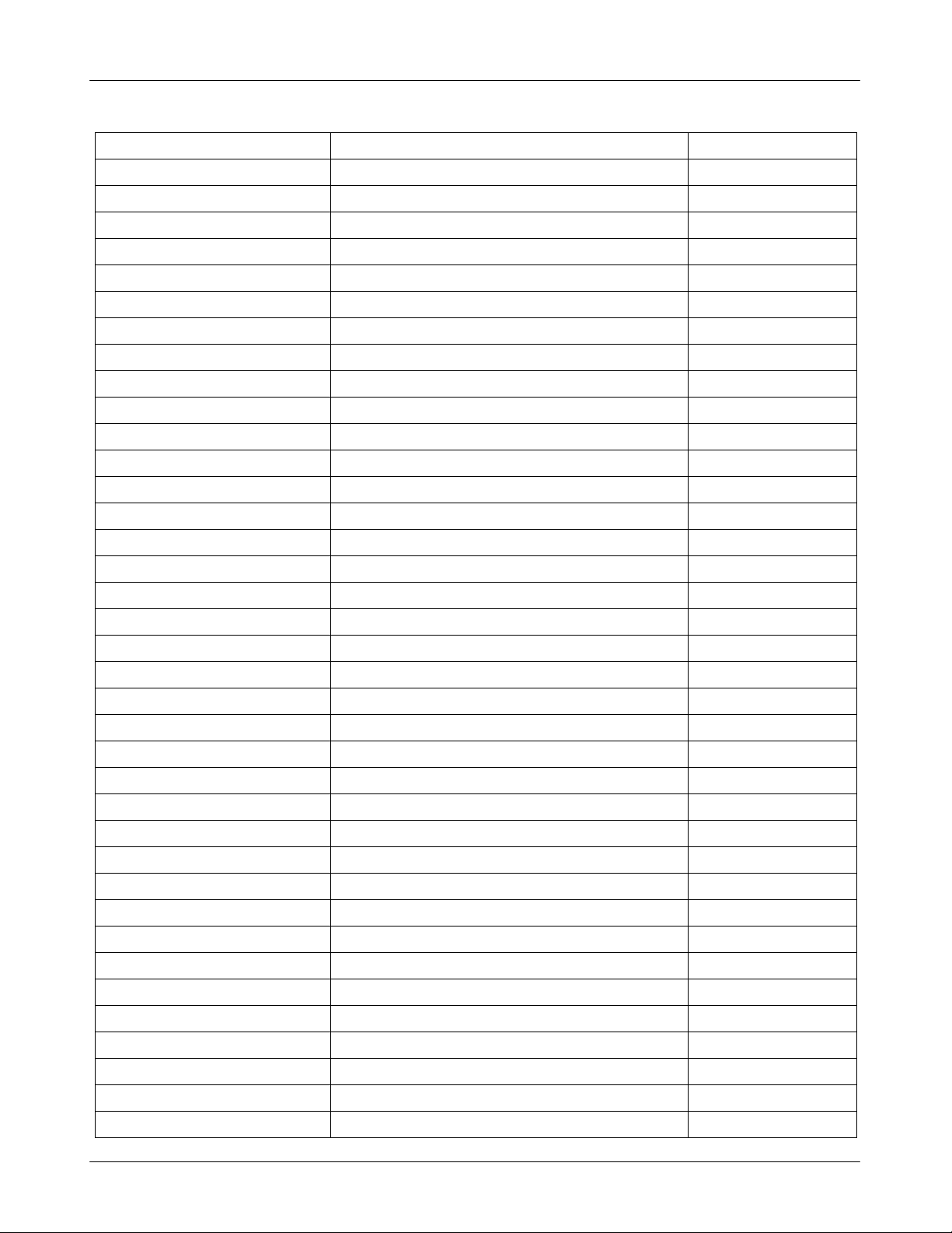
Electrical Part List
Design LOC Description SEC CODE
R407,R408,R612 R-CHIP 2007-000140
R414,R415,R702 R-CHIP 2007-000173
R416,R515,R517,R520 R-CHIP 2007-000171
R502,R734 R-CHIP 2007-000168
R503 R-CHIP 2007-003010
R507 R-CHIP 2007-000165
R510,R747,R748 R-CHIP 2007-000159
R522,R525,R528,R530 R-CHIP 2007-000171
R543,R705 R-CHIP 2007-000141
R601,R602,R603,R604 R-CHIP 2007-000171
R605,R606,R607,R608 R-CHIP 2007-000171
R613,R633,R634 R-CHIP 2007-001217
R614,R620 R-CHIP 2007-001290
R615,R616,R623,R624 R-CHIP 2007-000139
R617,R628,R630,R632 R-CHIP 2007-000138
R618 R-CHIP 2007-000145
R619 R-CHIP 2007-001325
R621 R-CHIP 2007-001306
R622 R-CHIP 2007-001301
R625 R-CHIP 2007-000147
R626 R-CHIP 2007-007142
R627,R717,R725,R728 R-CHIP 2007-000171
R629,R706 R-CHIP 2007-007491
R703,R707,R710 R-CHIP 2007-000138
R704 R-CHIP 2007-001156
R708 R-CHIP 2007-002965
R709 R-CHIP 2007-007306
R711,R716 R-CHIP 2007-001284
R713 R-CHIP 2007-007001
R714 R-CHIP 2007-000142
R715 R-CHIP 2007-000144
R720,R758,R765,R115 R-CHIP 2007-000162
R724,R726,R727,R730 R-CHIP 2007-000156
R729,R732,R733,R738 R-CHIP 2007-000171
R741,R743,R754,R755 R-CHIP 2007-000171
R757 R-CHIP 2007-001119
R759,R760,R761,R762 R-CHIP 2007-007021
4-6
SAMSUNG Proprietary-Contents may change without notice
This Document can not be used without Samsung's authorization
Electrical Part List
Design LOC Description SEC CODE
R763,R737 R-CHIP 2007-000148
R768,R769,R770 R-CHIP 2007-000171
RFSW601 RF CONNECTOR 3705-001355
TH100 NCP 1404-001224
U100 MSM 1205-002527
U201 POWER CHIP 1203-003335
U202 MIC2212-GMBML 1203-002969
U203 MIC2211-PSBML 1203-002860
U204 USBUF01W6 0407-001038
U301 FILTER NEW-ITEM013
U302 AUDIO CHIP 1204-002316
U501,U704 STG3699AQTR 1001-001306
U510 TC75S56FE 1202-001068
U600 ANTENNA SWITCH NEW-ITEM008
U601 BT Module NEW-ITEM001
U602 RTR6250 NEW-ITEM010
U603 GSM PAM 1201-002218
U701 WCDMA PAM 1201-002219
U702 RFL6200 1201-001984
U703 RFR 1205-002297
U705 STG3684QTR 1001-001248
U706 FSA4157L6X 1001-001265
U709 COMP-SMD NEW-ITEM002
U710 AMP NEW-ITEM011
U711 MIC5205-2.7BM5 1203-002565
U712 R1141Q181DTR 1203-003208
X200 CC7V-T1A-32.768K NEW-ITEM007
ZD402,ZD407,ZD409 DIODE-ZENER 0403-001387
ZD403,ZD404 DIODE-ZENER 0406-001190
ZD405,ZD406,ZD408 DIODE-ZENER 0406-001197
ZD410 DIODE-ZENER 0403-001387
ZD411 DIODE-ZENER 0406-001197
4-7
SAMSUNG Proprietary-Contents may change without notice
This Document can not be used without Samsung's authorization

Electrical Part List
4-8
SAMSUNG Proprietary-Contents may change without notice
This Document can not be used without Samsung's authorization
 Loading...