

Page 1
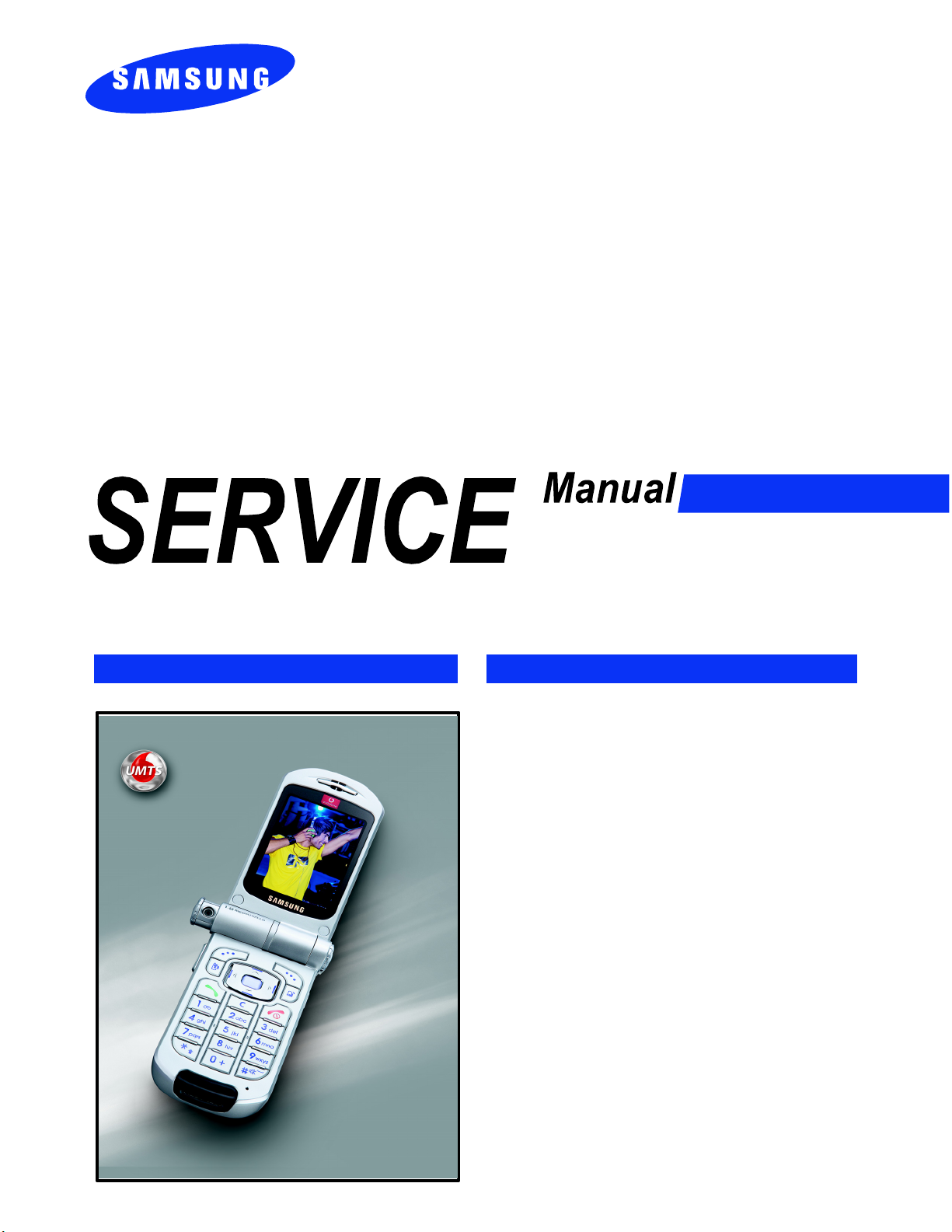
UMTS TELEPHONE
SGH-Z110V
UMTS TELEPHONE
CONTENTS
1. Specification
2. Circuit Description
3. Exploded Views and Parts List
4. Electrical Parts List
5. Block Diagrams
6. PCB Diagrams
7. Flow Chart of Troubleshooting
Page 2
This Service Manual is a property of Samsung Electronics Co.,Ltd.
Any unauthorized use of Manual can be punished under applicable
International and/or domestic law.
ⓒ
Samsung Electronics Co.,Ltd. Nov. 2004
Samsung Electronics Co.,Ltd. Nov. 2004
Printed in South Korea.
Printed in South Korea.
Code No.:
BASIC.
GH68-05795A
Page 3
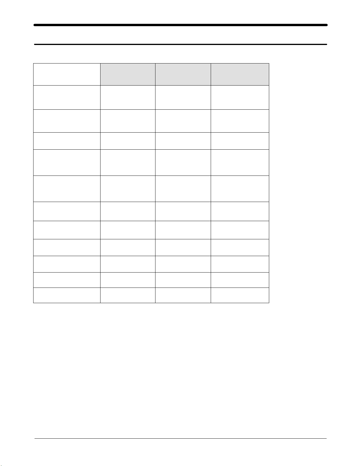
1. SGH-Z110V Specification
1. GSM General Specification
GSM900
Phase 1
Freq. Band[MHz]
Uplink/Downlink
ARFCN range 1~124
Tx/Rx spacing 45MHz 45MHz 95MHz
Mod. Bit rate/
Bit Period
Time Slot
Period/Frame
Period
Modulation 0.3GMSK 0.3GMSK 0.3GMSK
MS Power 33dBm~13dBm 33dBm~5dBm 30dBm~0dBm
890~915
935~960
270.833kbps
3.692us
576.9us
4.615ms
EGSM 900
Phase 2
880~915
925~960
0~124 &
975~1023
270.833kbps
3.692us
576.9us
4.615ms
DCS1800
Phase 1
1710~1785
1805~1880
512~885
270.833kbps
3.692us
576.9us
4.615ms
Power Class 5pcl ~ 15pcl 5pcl ~ 19pcl 0pcl ~ 15pcl
Sensitivity -102dBm -102dBm -100dBm
TDMA Mux 8 8 8
Cell Radius 35Km 35Km 2Km
1-1
SAMSUNG Proprietary-Contents may change without notice
This Document can not be used without Samsung's authorization
Page 4
Specification
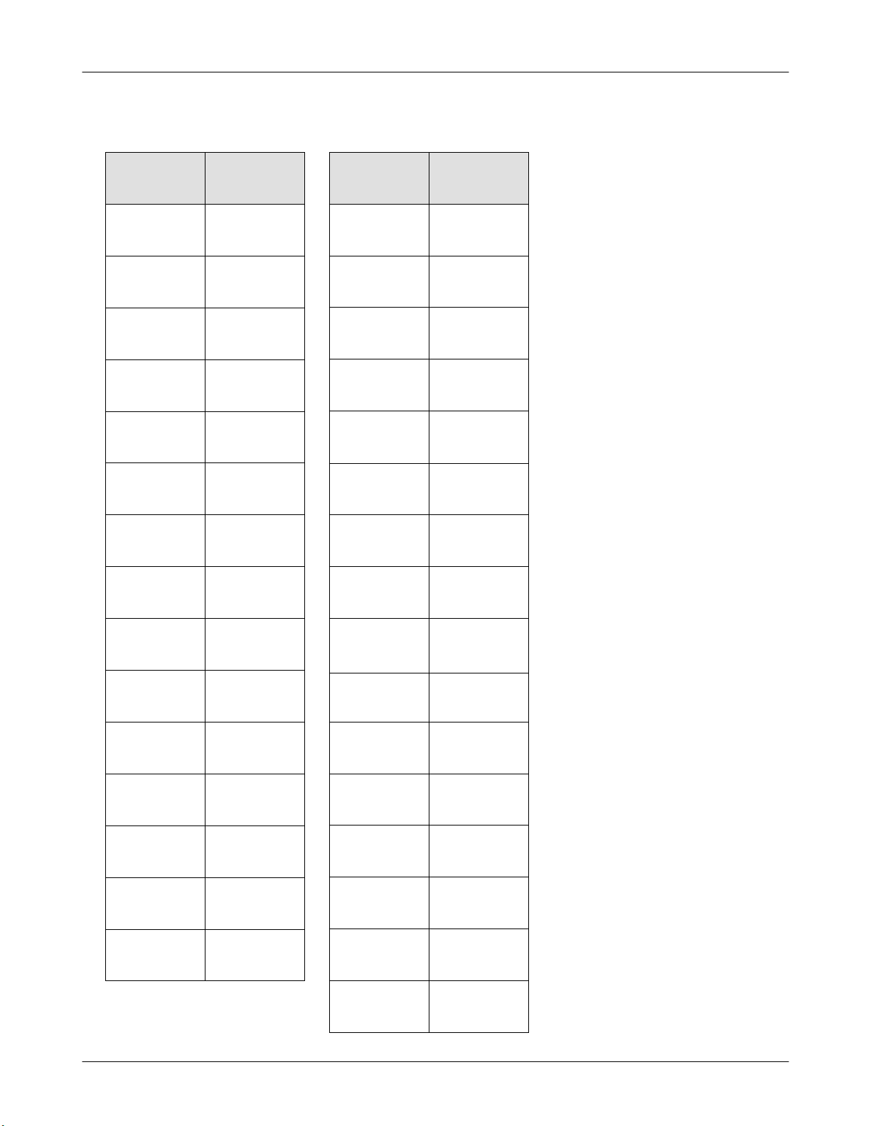
2. GSM TX power class
TX Pow er
control level
5 33±2 dBm
6 31±2 dBm
7 29±2 dBm
8 27±2 dBm
9 25±2 dBm
10 23±2 dBm
11 21±2 dBm
GSM900
TX Pow er
DCS1800
control level
0 30±3 dBm
1 28±3 dBm
2 26±3 dBm
3 24±3 dBm
4 22±3 dBm
5 20±3 dBm
6 18±3 dBm
12 19±2 dBm
13 17±2 dBm
14 15±2 dBm
15 13±2 dBm
16 11±3 dBm
17 9±3dBm
18 7±3 dBm
19 5±3 dBm
7 16±3 dBm
8 14±3 dBm
9 12±4 dBm
10 10±4 dBm
11 8±4dBm
12 6±4 dBm
13 4±4 dBm
14 2±5 dBm
15 0±5 dBm
1-2
SAMSUNG Proprietary-Contents may change without notice
This Document can not be used without Samsung's authorization
Page 5

2. SGH-Z110V Circuit Description
1. SGH-Z110V RF Circuit Description
1. Antenna Switch Module (U100)
The antenna switch module allows multiple operating bands and modes to share the same antenna. A common
antenna connects to one of five paths: 1) UMTS-2100 Rx/Tx, 2) EGSM-900 Rx, 3) EGSM-900 Tx, 4) DCS-1800 Rx,
and 5) DCS-1800 Tx. UMTS operation requires simultaneous reception and transmission.
2. Filter
To convert Electromagnetic Field Wave to Acoustic Wave and then pass the specific frequency band.
- GSM Rx FILTER (F100)→For filtering the frequency band between 925 ~ 960 MHz.
- DCS Rx FILTER (F101)→For filtering the frequency band 1805 and 1880 MHz.
- WCDMA Rx FILTER (F200)→For filtering the frequency band 2110 and 2170 MHz.
- WCDMA Tx FILTER (F201)→For filtering the frequency band 1920 and 1980 MHz.
3. VCTCXO (OSC200)
To generate the 19.2MHz reference clock to drive the logic and RF.
4. Duplexer (F202)
A duplexer splits a single operating band into receive and transmit paths.
5. WCDMA PAM (U201)
This is a key component in the transmitter chain and must complement the RTR6200 IC precisely; jointly they
dominate the UMTS transmitter performance characteristics. Parameters such as gain, output power level, ACLR,
harmonics, Rx-band noise, and power supply current are critical.
6. GSM/DCS PAM (U102)
The PAM is a key component in any transmitter chain and must complement the rest of the transmitter precisely.
For GSM and DCS operation, the closed-loop transmit power control functions add even more requirements relative
to the UMTS PA. In addition to gain control and switching requirements, the usual RF parameters such as gain,
output power level, several output spectrum requirements, and power supply current are critical.
7. GSM/DCS Dual Tx VCO (OSC100)
The dual Tx VCO outputs, one for EGSM and one for DCS, drive a resistive network that splits the active signal
into two signals: 1) the input to the active PAM – this is the low loss path, and 2) the OPLL feedback signal.
8. Dual VCO (OSC201)
The dual-band UHF VCO is a key component within its phase-locked loop; VCO performance directly impacts PLL
and transceiver performance. GSM/DCS Rx/Tx LO & UMTS Rx LO signal is generated from this dual VCO's output.
9. RFL6200 (U200)
The RFL6200 includes an LNA circuit optimized for UMTS-2100 operation. The LNA is separated from all other
receive functions contained within the RFR6200 receiver IC to improve mixer LO to RF isolation – a critical
parameter in the Zero-IF architecture.
2-1
SAMSUNG Proprietary-Contents may change without notice
This Document can not be used without Samsung's authorization
Page 6

Circuit Description
10. RFR6200 (U203)
The RFR6200 provides the Zero-IF receiver signal path, from RF to analog baseband, for UMTS-2100 applications.
The RFR6200 accepts its UMTS input signal from the handset RF front-end design. The UMTS input is configured
differentially to optimize second-order inter-modulation and common mode rejection performance, and implements
MSM-controlled gain adjustments to extend the receiver dynamic range.
11. RTR6200 (U101)
The RTR6200 supports multi-band, multi-mode phones with two receiver signal paths and three transmitter signal
paths:
1) Receiver paths
- EGSM-900
- DCS-1800
2) Transmitter paths
- EGSM-900 (using OPLL technique)
- DCS-1800 (using OPLL technique)
- UMTS-2100
Numerous secondary functions are integrated on-chip as well:
3) Phase-locked loop circuits
- PLL#1 and an on-chip VCO supports UMTS Tx
- PLL#2 and an external VCO supports EGSM Rx and Tx, DCS Rx and Tx, and UMTS Rx
4) Transceiver LO generation and distribution circuits
- EGSM-900 Rx and Tx
- DCS-1800 Rx and Tx
- UMTS-2100 Tx
2-2
SAMSUNG Proprietary-Contents may change without notice
This Document can not be used without Samsung's authorization
Page 7

Circuit Description
2. Baseband Circuit description of SGH-Z110V
1. PM6050
1.1. Power Management
Ten low-dropout regulators designed specifically for GSM applications power the terminal and help ensure optimal
system performance and long battery life. It provides seven LDO support for 2.6V, 2.8V while a self-resetting,
electronically fused switch supplies power to external accessories. Ancillary support functions, such as RTC module
and RTC charger, Clock Buffer, aid in reducing both board area and system complexity.
SBI BUS serial interface provides access to control and configuration registers. This interface gives full control of
the MSM6200 and enables system designers to maximize both standby and talk times.
Supervisory functions. including a reset generator, an input voltage monitor, and a ADC support reliable system
design. These functions work together to ensure proper system behavior during start-up or in the event of a fault
condition(low microprocessor voltage, insufficient battery energy, or excessive die temperature).
1.2 TCXO Controller and Buffers
The PM6050 IC includes circuits for controlling the TCXO warm-up and buffering its signal for distribution throughout
the handset. Performance specifications are presented below.
2. Connector
2-1. LCD Connector
LCD is consisted of main LCD(color 262K TFT LCD) and small LCD(color 65K TFT LCD). Chip select signals in the
MA55141(U501), SLCD_CS can enable small LCD and DEN for main LCD. I2C buses in MSM6200 (U301) control
white-LED of LCDs.
"SLCD_RESET, MLCD_RESET" signals initiate the Reset process of LCDs.
8-bit data lines(RGB[10:17]) transfers data and commands to Small LCD through bypass capacitor. Data and
commands use "SCLD_RS" signal. If this signal is high, Inputs to Small LCD are commands. If it is low, Inputs to
Small LCD are data. The signal which informs the input or output state to Small LCD, is required.
Main LCD interface is 18bit data lines(RGB[0:17]) CPU Interface.
"RGB_VSYNC","RGB_HSYNC","RGB_DE",and,"RGB_CLK" are the signal for transferring data.
Power signals for LCD are "2.8VDV" and "VBATT". "SPKR_P","SPKL_P", "SPKR_N" and "SPKL_N" from U602 are
used for dual audio speaker.
2-2. Key
This is consisted of key interface pins among U301, KEY_0~3 and SCAN_0~6. These signals compose the matrix.
Result of the matrix informs the key status to key interface in U301. Power on/off key is seperated from the matrix.
So power on/off signal is connected with U301 to enable U400. Eighteen key LED use the "VCC_BK" supply voltage
from U304. "HALL_SW" informs the status of folder (open or closed) to modem. This uses the hall effect IC,EM1681.
A magnet under main LCD enables EM1681. It has additional two hall-effect ICs, that are needed for camera
sensing.
One senses the rotation of Z110V camera, and the other senses the Push-pull of the camera.
2-3
SAMSUNG Proprietary-Contents may change without notice
This Document can not be used without Samsung's authorization
Page 8

Circuit Description
2-3. EMI ESD Filter
This system uses the EMI ESD filter, GMF05LC to protect ESD and Noise from IF CONNECTOR part, LCD,
Camra, and KEY PCB.
2-4. IF connetor
It is 24-pin connector. They are designed to use VBATT, VF, Q_TXD0, Q_RXD0, JIG_ON, M_RXD0, M_TXD0, USB
signal(D+,D-,USB_VCC) and GND. They connected to power supply IC, microprocessor and signal processor IC.
3. Audio
RCV_P and RCV_N from U601 are connected to the main receiver. EAR10P and EAR10N are connected to the
Earphone receiver. MIC1P and MIC1N are connected to the main MIC. And MIC2P and MIC2N are connected to
the Earphone.
YMU769 has a virtual speaker image function, so that it is the most suitable LSI as a sound source output device
which is used in mobile phones for high functional game sounds or high quality ringing melodies, and so on.
Synthesizer section in YMU769 adopts the “Stereophonic Hybrid Synthesizer System” that is given the advantages
of both FM Synthesizers and Wave Table Synthesizers, makes it possible to generate up to 32 FM voices and 32
wave table voices simultaneously.
YMU769 is a LSI for portable telephone that is capable of playing high quality music by utilizing FM synthesizer and
ADPCM decoder that are included in this device.
As a synthesis, YMU769 is equipped 32 voices with different tones. Since the device is capable of simultaneously
generating up to synchronous with the play of the FM synthesizer, various sampled voices can be used as sound
effects. Since the play data of YMU769 is interpreted at anytime through data bus, the length of the data(playing
period) is not limited, so the device can flexibly support application such as incoming call melody music distribution
service.
The hardware sequence built in this device allows playing of the complex music without giving excessive load to the
CPU of the portable telephones. Moreover, the registers of the FM synthesizer can be operated directly for real time
sound generation, allowing, for example, utilization of various sound effects when using the game software installed
in the portable telephone.
YMU769 includes a speaker amplifier with high ripple removal rate whose maximum output is 550mW (SPVDD=3.6V).
For the headphone, it is provided with a stereophonic output terminal.
4. Memory
The signals in the MSM6200 enable two memories. They use only one volt supply voltage, VDD_LP from the
PM6050. This system uses SPANSION's memory, S99PL129JCOBAWUC. It is consisted of 128M bits flash NOR
memory and 32M bits SRAM memory. It has 16 bit data line, AD[0~15] which is connected to MSM6200. It has 22
bit address lines, A[1~22]. ROM_CS and RAM_CS signals is chip select.
In the multi-media processor, it has two type of memories. One is 1GMbit NAND Flash memory and the other is
512Mbit SDRAM memory. Multi-media processor doesn't have a NAND memory interface. But we make a software
algorithm use for NAND memory.
2-4
SAMSUNG Proprietary-Contents may change without notice
This Document can not be used without Samsung's authorization
Page 9

Circuit Description
5. Multi-media processor MA55141
MA55141 is an LSI, which is designed on 3GPP 3G-324M Standard for a video telephone system.
Since protocol software is external, MA55141 can run with another protocol like H.323 by changing its software.
MA55141 has ARM9 CPU, so supports more various application.
Feature
- Based on 3GPP 3G-324M standard
- Video MPEG-4 (simple profile level1) or H263 (baseline)
- Audio AMR, G723.1, MP3 or AAC (program downloadable)
- Multiplexing H.223 (Level 0, 1, 2, processed by CPU with assistant hardware)
- Control H.245 (Processed all by CPU)
- Built-in 32bit RISC CPU(ARM926EJ) for control. (Max 133MHz, I-cache 16KB, D-cache 8KB, MMU and JAVA
accelerator (Jazelle) included.)
- Built-in 16bit DSP for audio CODEC
- Built-in SD/MMC/Memory Stick I/F
- Video input Rec601/656 YUV = 4:2:2, 8 bit I/F
- Video output Rec601 YUV = 4:2:2(8bit) / RGB 18bit
Built-in Picture-In-Picture Image Displaying Functions
Built-in On Screen Display(OSD) Functions with alpha blending
- Video CODEC
Encoding and decoding : QCIF 40fps, CIF 10fps
Encoding only : QCIF 68fps, CIF 17fps
Decoding only : QCIF 96fps, CIF 24fps
Deblocking filter is built-in.
Max output image size : 2032×2032
- Program on SDRAM is executable without ROM (optional).
- Power supply
VDDI1=1.425V to 1.65V (For internal circuit. Please power off during stand-by)
VDDI2=VDDI1 (For internal circuit. Please provide during stand-by)
VDDP0, VDDP1=1.425V to 1.65V (For internal PLL0 and PLL1)
VDDO, VDDOD=2.7V to 3.0V (For I/O)
- Max operating frequency CPU clock = 133MHz
DSP clock = 100MHz
SDRAM clock = 100MHz
Video clock = SDRAM clock/2
6. MIC2211 (U604/U605)
This LDO is the voltage source of Multimedia part. The MIC2211 is a dual-output LDO regulator.
The one of dual is capable of sourcing 150mA, while the another one can supply up to 300mA.
Ideal for battery operated applications, the MIC2211 offers 1% accuracy, extremely low dropout voltage (80mV @
100mA), and extremely low ground current (only 48mA total). Equipped with TTL logic compatible enable pins, the
MIC2211 can be put into a zero-off-mode current state, drawing no current when disabled. Separate enable pins
allow individual control of each output voltage.
2-5
SAMSUNG Proprietary-Contents may change without notice
This Document can not be used without Samsung's authorization
Page 10

Circuit Description
7. Camera (HV7151SP)
The HV7151SP is a highly integrated single chip CMOS color image sensor implemented by proprietary
Hynix 0.35um COMS sensor process realizing high sensitivity and wide dynamic range.
Total pixel array size is 1170 x 880 pixels are active. So, It can supports the picture below 1Mega-pixel snap shot.
Each active pixel composed of 4 transistors has a micro-lens to enhance sensitivity, and converts photon energy to
analog pixel voltage. On-chip 10bit Analog to Digital Converter(ADC) ditgitizes analog pixel voltage, and on-chip
Correlated Double Sampling(CDS) scheme reduces Fixed Pattern Noise(FPN) dramatically. The integration of sensor
function and image processing functions make HV7151SP especially very suitable for mobile imaging systems such
as IMT-2000.
8. Irda
This system uses IRDA module, HSDL_3208, Agilent's. This has signals, Input data and output data.
These signals are connected to MSN6200.
2-6
SAMSUNG Proprietary-Contents may change without notice
This Document can not be used without Samsung's authorization
Page 11
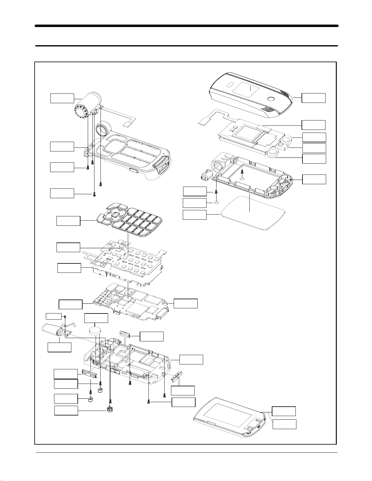
3. SGH-Z110V Exploded View and its Parts list
1. Cellular phone Exploded View
QCA01
QFR01
QCR42
QCR12
QKP01
QME01
QSH02
QFU01
QLC01
QSP02
QSP01
QSP03
QFL01
QCR20
QSC14
QMW01
QCR05
QAN01
QVO01
QCR26
QSC13
QRF01
QMP01
QMI01
QMO01
QVO02
QRE01
QIF01
QCR07
QBA32
QBA33
3-1
SAMSUNG Proprietary-Contents may change without notice
This Document can not be used without Samsung's authorization
Page 12
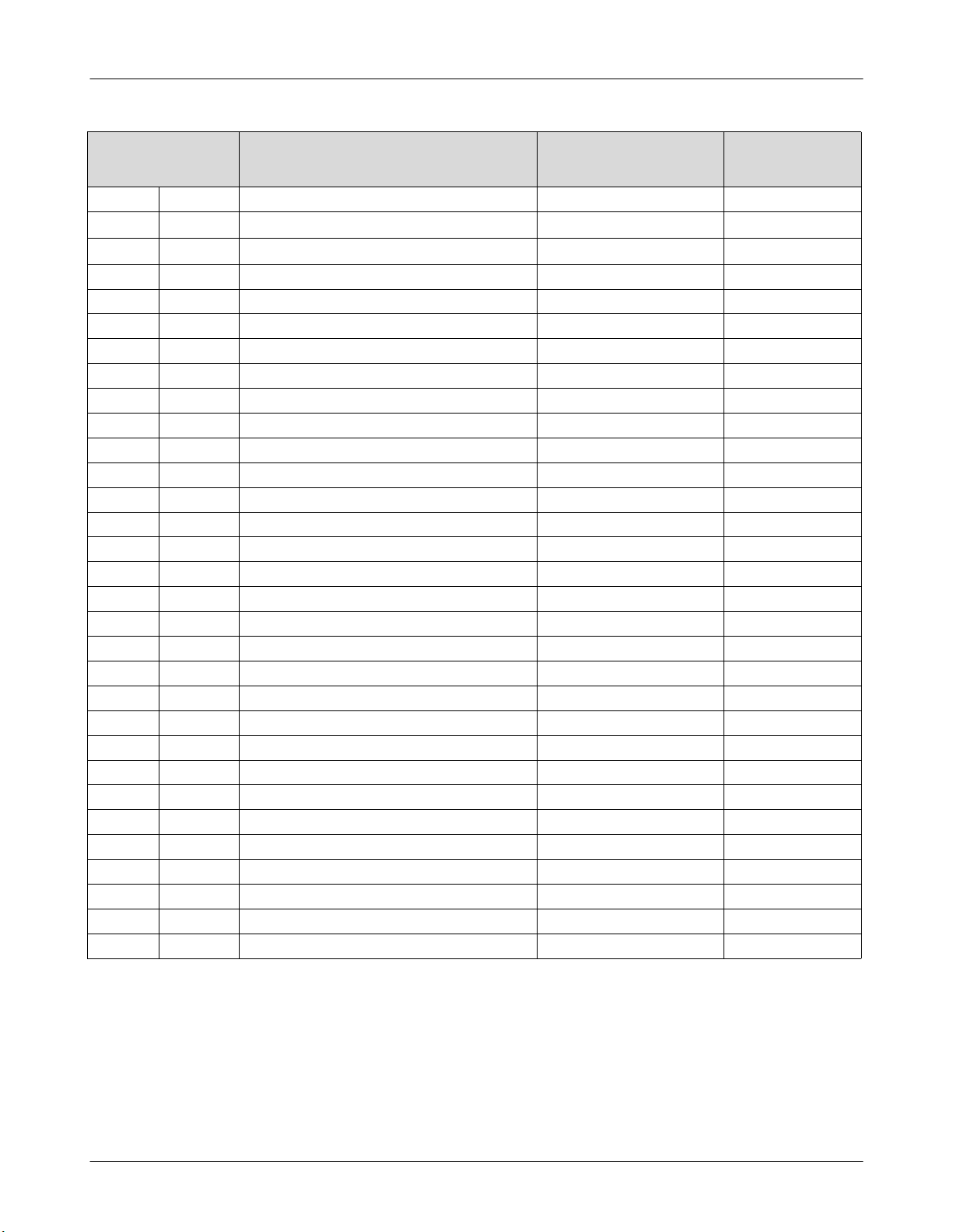
Exploded view and its Part list
2. Cellular phone Parts list
Location
NO.
QFU01 FOLDER UPPER GH75-05245A
QLC01 LCD GH07-00614A
QSP01 SPEAKER 3001-001540
QSP02 SPEAKER 3001-001622
QSP03 SPEAKER 3001-001623
QFL01 FOLDER LOWER GH75-05246A
QCR20 SCREW 6001-001429
QSC14 FOLDER SCREW SHEET GH74-10909A
QMW01 MAIN WINDOW LCD GH72-16368A
QFR01 FRONT COVER GH75-05243A
QCA01 CAMERA GH59-01767A
QCR12 SCREW 6001-001530
QKP01 KEYPAD GH75-05247A
QME01 UNIT KEYPAD GH59-01768A
QSH02 SHIELD COVER GH71-04036A
QMP01 MAIN PBA GH92-01730A
QMI01 MICROPHONE ASSY GH30-00143A
QCR05 SCREW 6001-001478
QMO01 MOTOR 3101-001415
QVO02 KEY REJECT GH72-15405A
QVO01 KEY VOL GH72-15407A
QAN01 ANTENNA GH42-00488A
QRE01 REAR COVER GH75-05244A
QSC13 REAR SCREW CAP GH72-17726A
QRF01 RF COVER GH72-15400A
QIF01 IF COVER GH72-15401A
QCR07 SCREW 6001-001691
QCR26 SCREW 6001-001850
QCR42 SCREW 6001-001300
QBA32 BATTERY-860MAH GH43-01529A
QBA33 BATTERY-1360MAH GH43-01530A
Description SEC CODE Remark
3-2
SAMSUNG Proprietary-Contents may change without notice
This Document can not be used without Samsung's authorization
Page 13
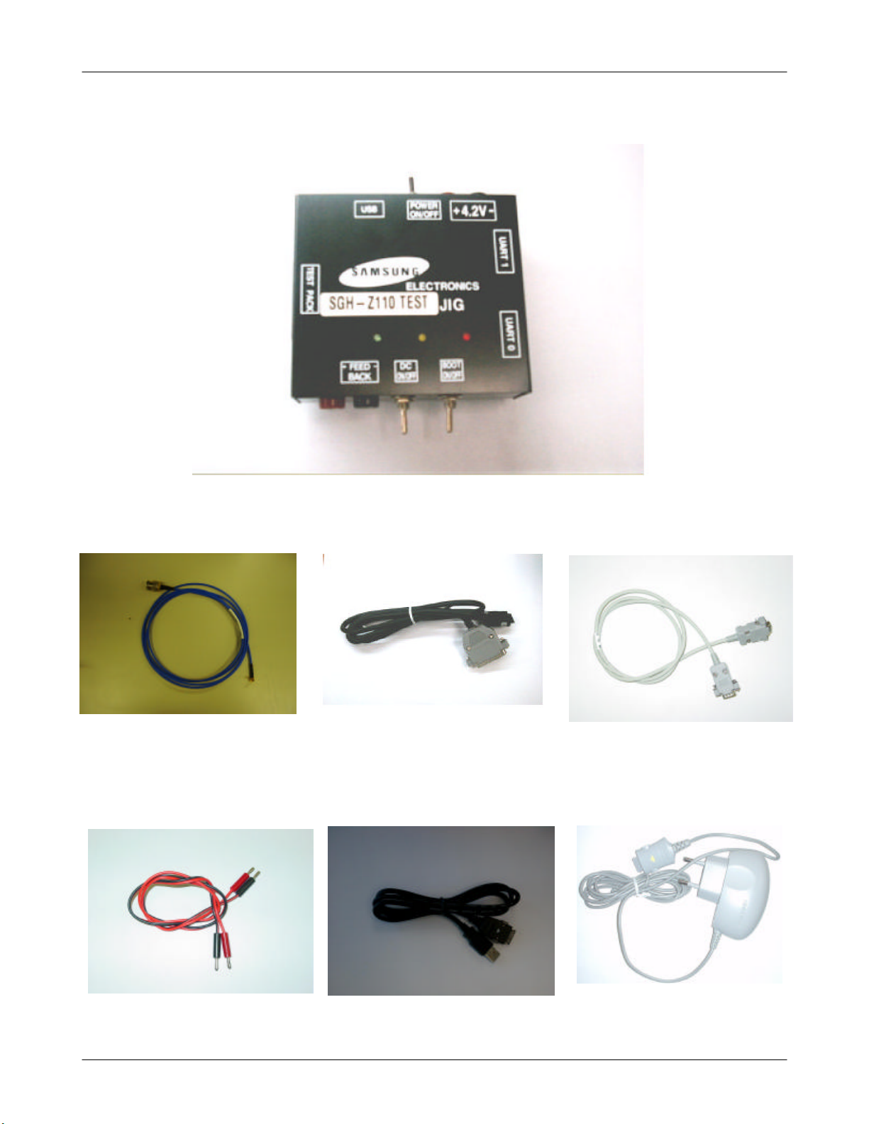
3. Test Jig (GH80-03308A)
Exploded view and its Part list
3-1. RF Test Cable
(GH39-00105A)
3-4. Power Supply Cable
3-2. Test Cable
(GH39-00337E)
3-5. DATA CABLE
(GH39-00326A)
3-3. Serial Cable
3-6. TC
(GH44-00701A)
3-3
SAMSUNG Proprietary-Contents may change without notice
This Document can not be used without Samsung's authorization
Page 14
4. SGH-V110V MAIN Electrical Parts List
SEC Code Design LOC
0403-001387 ZD303
0403-001427 ZD304
0404-001153 ZD401
0404-001167 ZD308
0406-001178 ZD307
0406-001197 ZD300
0406-001197 ZD301
0406-001197 ZD302
0406-001197 ZD305
0406-001197 ZD400
0406-001197 ZD403
0406-001197 ZD404
0406-001197 ZD700
0406-001197 ZD701
0406-001197 ZD702
0406-001197 ZD703
0406-001197 ZD704
0406-001197 ZD705
0406-001197 ZD706
0406-001197 ZD707
0406-001197 ZD708
0406-001197 ZD709
0406-001197 ZD710
0406-001197 ZD711
0406-001197 ZD712
0406-001197 ZD713
0406-001197 ZD714
0406-001197 ZD715
0406-001197 ZD716
0406-001197 ZD717
0407-001002 ZD306
0407-001002 ZD402
0407-001038 U307
0504-001060 U202
0504-001113 Q201
0505-001423 U303
0505-001423 U305
0505-001423 U313
0505-001423 U608
SEC Code Design LOC
0505-001464 Q200
0505-001464 Q300
0604-001261 LED700
1001-001231 U205
1001-001231 U312
1001-001231 U402
1001-001288 U100
1001-001296 U306
1001-001296 U503
1001-001296 U601
1001-001306 U404
1109-001302 U300
1109-001317 U500
1201-001984 U200
1201-002174 U102
1201-002196 U201
1203-003007 U400
1203-003105 U302
1203-003105 U304
1203-003137 U403
1203-003275 U605
1203-003322 U604
1203-003359 U607
1203-003501 U401
1203-003563 U310
1203-003585 U700
1203-003591 U204
1204-002316 U602
1204-002354 U501
1205-002295 U301
1205-002297 U203
1205-002300 U101
1205-002530 U606
1205-002592 U308
1404-001224 TH300
1405-001082 V602
1405-001082 V603
2007-000138 R123
2007-000138 R202
4-1
SAMSUNG Proprietary-Contents may change without notice
This Document can not be used without Samsung's authorization
Page 15
Electrical Parts List
SEC Code Design LOC
2007-000138 R209
2007-000140 R351
2007-000147 R125
2007-000148 R105
2007-000148 R111
2007-000148 R331
2007-000149 R352
2007-000160 R631
2007-000168 R321
2007-000171 R204
2007-000171 R205
2007-000171 R220
2007-000171 R628
2007-000171 R633
2007-000172 R112
2007-000173 R201
2007-000174 R733
2007-000242 R348
2007-000775 R408
2007-001119 R353
2007-001217 R113
2007-001217 R127
2007-001217 R128
2007-001284 R212
2007-001291 R114
2007-001291 R115
2007-001291 R224
2007-001291 R225
2007-001295 R116
2007-001298 R210
2007-001298 R211
2007-001301 R122
2007-001305 R121
2007-001307 R117
2007-001307 R118
2007-001307 R119
2007-001307 R120
2007-001313 R316
2007-001325 R109
SEC Code Design LOC
2007-001325 R607
2007-001339 R320
2007-001339 R322
2007-002796 R410
2007-002796 R514
2007-003006 R420
2007-003022 R731
2007-003022 R732
2007-007107 R219
2007-007107 R412
2007-007135 R334
2007-007137 R218
2007-007142 R126
2007-007314 R200
2007-007314 R206
2007-007314 R208
2007-007314 R333
2007-007318 R330
2007-007318 R615
2007-007318 R616
2007-007491 R110
2007-007491 R207
2007-007538 R327
2007-007698 R216
2007-007981 R421
2007-008045 R107
2007-008045 R124
2007-008045 R129
2007-008045 R306
2007-008045 R307
2007-008045 R308
2007-008045 R309
2007-008045 R700
2007-008045 R701
2007-008045 R702
2007-008045 R703
2007-008045 R704
2007-008045 R705
2007-008045 R706
4-2
SAMSUNG Proprietary-Contents may change without notice
This Document can not be used without Samsung's authorization
Page 16
Electrical Parts List
SEC Code Design LOC
2007-008045 R707
2007-008045 R708
2007-008045 R709
2007-008045 R710
2007-008045 R711
2007-008045 R712
2007-008045 R713
2007-008045 R714
2007-008045 R715
2007-008045 R716
2007-008045 R717
2007-008045 R718
2007-008045 R719
2007-008045 R720
2007-008045 R721
2007-008045 R722
2007-008045 R723
2007-008045 R724
2007-008045 R725
2007-008055 R405
2007-008055 R415
2007-008055 R618
2007-008055 R621
2007-008055 R622
2007-008055 R626
2007-008055 R727
2007-008117 R215
2007-008117 R612
2007-008117 R613
2007-008213 R510
2007-008213 R511
2007-008401 R419
2007-008419 R100
2007-008419 R103
2007-008419 R106
2007-008419 R108
2007-008419 R214
2007-008419 R217
2007-008419 R305
SEC Code Design LOC
2007-008419 R328
2007-008419 R350
2007-008419 R400
2007-008419 R404
2007-008419 R413
2007-008419 R417
2007-008419 R629
2007-008419 R630
2007-008483 R213
2007-008483 R301
2007-008483 R302
2007-008483 R346
2007-008483 R347
2007-008483 R349
2007-008483 R358
2007-008483 R502
2007-008483 R728
2007-008483 R729
2007-008483 R730
2007-008516 R300
2007-008516 R317
2007-008516 R318
2007-008516 R354
2007-008516 R356
2007-008516 R406
2007-008516 R418
2007-008516 R517
2007-008516 R518
2007-008516 R519
2007-008531 R101
2007-008542 R221
2007-008542 R303
2007-008542 R304
2007-008542 R310
2007-008542 R311
2007-008542 R312
2007-008542 R313
2007-008542 R314
2007-008542 R315
4-3
SAMSUNG Proprietary-Contents may change without notice
This Document can not be used without Samsung's authorization
Page 17
Electrical Parts List
SEC Code Design LOC
2007-008542 R323
2007-008542 R324
2007-008542 R326
2007-008542 R332
2007-008542 R335
2007-008542 R336
2007-008542 R337
2007-008542 R340
2007-008542 R341
2007-008542 R345
2007-008542 R355
2007-008542 R357
2007-008542 R360
2007-008542 R409
2007-008542 R500
2007-008542 R504
2007-008542 R507
2007-008542 R508
2007-008542 R509
2007-008542 R512
2007-008542 R513
2007-008542 R601
2007-008542 R603
2007-008542 R606
2007-008542 R608
2007-008542 R609
2007-008542 R610
2007-008542 R625
2007-008542 R632
2007-008542 R739
2007-008548 R401
2007-008548 R403
2007-008548 R414
2007-008548 R416
2007-008648 R407
2007-008648 R619
2007-008648 R620
2007-008648 R623
2007-008648 R624
SEC Code Design LOC
2007-009081 R223
2007-009122 R222
2203-000138 C162
2203-000233 C200
2203-000233 C209
2203-000233 C228
2203-000233 C653
2203-000254 C101
2203-000254 C348
2203-000254 C350
2203-000254 C426
2203-000254 C620
2203-000254 C621
2203-000254 C638
2203-000254 C659
2203-000311 C163
2203-000330 C208
2203-000330 C210
2203-000330 C214
2203-000330 C242
2203-000359 C107
2203-000359 C109
2203-000359 C112
2203-000359 C113
2203-000386 C104
2203-000386 C327
2203-000386 C329
2203-000438 C103
2203-000438 C135
2203-000438 C160
2203-000438 C231
2203-000438 C448
2203-000489 C325
2203-000530 C141
2203-000628 C472
2203-000654 C148
2203-000679 C341
2203-000696 C146
2203-000696 C151
4-4
SAMSUNG Proprietary-Contents may change without notice
This Document can not be used without Samsung's authorization
Page 18
Electrical Parts List
SEC Code Design LOC
2203-000812 C102
2203-000812 C108
2203-000812 C150
2203-000812 C213
2203-000812 C248
2203-000854 C117
2203-000854 C122
2203-000854 C123
2203-000854 C134
2203-000885 C205
2203-000995 C211
2203-001124 C250
2203-001178 C212
2203-001259 C249
2203-001383 C221
2203-001405 C660
2203-002443 C172
2203-002677 C147
2203-005050 C256
2203-005050 C257
2203-005050 C410
2203-005234 C173
2203-005234 C178
2203-005288 C230
2203-005288 C236
2203-005393 C317
2203-005393 C318
2203-005480 C647
2203-005482 C100
2203-005482 C118
2203-005496 C658
2203-005503 C171
2203-005682 C114
2203-005682 C120
2203-005682 C124
2203-005682 C125
2203-005682 C126
2203-005682 C129
2203-005682 C130
SEC Code Design LOC
2203-005682 C138
2203-005682 C139
2203-005682 C140
2203-005682 C142
2203-005682 C144
2203-005682 C153
2203-005682 C169
2203-005682 C353
2203-005682 C354
2203-005682 C465
2203-005682 C478
2203-005682 C480
2203-005682 C666
2203-005682 C667
2203-005682 C668
2203-005682 C669
2203-005682 C670
2203-005682 C671
2203-005682 C672
2203-005682 C701
2203-005682 C708
2203-005682 C719
2203-005682 C720
2203-005682 C721
2203-005682 C722
2203-005717 C131
2203-005717 C132
2203-005717 C206
2203-005717 C485
2203-005717 C487
2203-005717 C488
2203-005717 C489
2203-005717 C491
2203-005717 C492
2203-005717 C494
2203-005717 C495
2203-005717 C498
2203-005717 C499
2203-005717 C700
4-5
SAMSUNG Proprietary-Contents may change without notice
This Document can not be used without Samsung's authorization
Page 19
Electrical Parts List
SEC Code Design LOC
2203-005717 C709
2203-005729 C158
2203-005729 C170
2203-005729 C175
2203-005729 C247
2203-005729 C258
2203-005729 C401
2203-005729 C403
2203-005729 C413
2203-005729 C415
2203-005729 C417
2203-005729 C450
2203-005729 C451
2203-005729 C453
2203-005729 C455
2203-005729 C458
2203-005729 C462
2203-005729 C467
2203-005729 C469
2203-005729 C477
2203-005729 C479
2203-005729 C481
2203-005729 C483
2203-005729 C603
2203-005729 C606
2203-005729 C609
2203-005736 C133
2203-005736 C176
2203-005736 C201
2203-005736 C223
2203-005736 C227
2203-005736 C238
2203-005736 C241
2203-005736 C244
2203-005736 C335
2203-005736 C344
2203-005736 C345
2203-005736 C346
2203-005736 C442
SEC Code Design LOC
2203-005736 C627
2203-005736 C628
2203-005736 C631
2203-005736 C635
2203-005779 C326
2203-005779 C328
2203-005779 C400
2203-005779 C405
2203-005779 C412
2203-005779 C414
2203-005779 C416
2203-005779 C452
2203-005779 C454
2203-005779 C459
2203-005779 C463
2203-005779 C468
2203-005779 C470
2203-005779 C476
2203-005779 C482
2203-005779 C604
2203-005779 C607
2203-005779 C611
2203-005806 C116
2203-005806 C119
2203-005806 C143
2203-005806 C155
2203-005806 C168
2203-005806 C174
2203-005806 C235
2203-005806 C253
2203-005806 C306
2203-005806 C314
2203-005806 C614
2203-006053 C342
2203-006053 C347
2203-006090 C474
2203-006090 C640
2203-006090 C652
2203-006093 C305
4-6
SAMSUNG Proprietary-Contents may change without notice
This Document can not be used without Samsung's authorization
Page 20
Electrical Parts List
SEC Code Design LOC
2203-006093 C310
2203-006093 C313
2203-006093 C331
2203-006093 C339
2203-006093 C427
2203-006093 C428
2203-006093 C432
2203-006093 C435
2203-006093 C456
2203-006093 C629
2203-006093 C630
2203-006093 C641
2203-006093 C651
2203-006093 C656
2203-006093 C703
2203-006120 C251
2203-006137 C167
2203-006190 C625
2203-006190 C626
2203-006194 C128
2203-006194 C137
2203-006194 C156
2203-006194 C159
2203-006194 C161
2203-006194 C177
2203-006194 C229
2203-006194 C233
2203-006194 C319
2203-006194 C321
2203-006194 C334
2203-006194 C338
2203-006201 C340
2203-006201 C352
2203-006201 C420
2203-006201 C433
2203-006201 C446
2203-006201 C457
2203-006201 C718
2203-006208 C154
2203-006208 C239
SEC Code Design LOC
2203-006208 C245
2203-006208 C254
2203-006208 C255
2203-006208 C351
2203-006208 C421
2203-006208 C422
2203-006208 C439
2203-006208 C473
2203-006208 C707
2203-006208 C713
2203-006208 C717
2203-006257 C706
2203-006305 C105
2203-006305 C203
2203-006305 C225
2203-006305 C304
2203-006305 C309
2203-006305 C312
2203-006305 C337
2203-006305 C423
2203-006305 C424
2203-006305 C425
2203-006305 C431
2203-006305 C434
2203-006305 C436
2203-006305 C440
2203-006305 C441
2203-006305 C447
2203-006305 C497
2203-006324 C207
2203-006379 C106
2203-006423 C115
2203-006423 C121
2203-006423 C127
2203-006423 C136
2203-006423 C145
2203-006423 C157
2203-006423 C165
2203-006423 C202
4-7
SAMSUNG Proprietary-Contents may change without notice
This Document can not be used without Samsung's authorization
Page 21
Electrical Parts List
SEC Code Design LOC
2203-006423 C224
2203-006423 C226
2203-006423 C232
2203-006423 C234
2203-006423 C237
2203-006423 C240
2203-006423 C243
2203-006423 C246
2203-006423 C300
2203-006423 C301
2203-006423 C302
2203-006423 C303
2203-006423 C307
2203-006423 C308
2203-006423 C311
2203-006423 C316
2203-006423 C320
2203-006423 C322
2203-006423 C323
2203-006423 C324
2203-006423 C330
2203-006423 C333
2203-006423 C336
2203-006423 C343
2203-006423 C349
2203-006423 C406
2203-006423 C407
2203-006423 C411
2203-006423 C419
2203-006423 C429
2203-006423 C430
2203-006423 C438
2203-006423 C445
2203-006423 C461
2203-006423 C466
2203-006423 C484
2203-006423 C486
2203-006423 C490
2203-006423 C500
SEC Code Design LOC
2203-006423 C501
2203-006423 C502
2203-006423 C503
2203-006423 C504
2203-006423 C505
2203-006423 C506
2203-006423 C507
2203-006423 C510
2203-006423 C515
2203-006423 C516
2203-006423 C517
2203-006423 C518
2203-006423 C519
2203-006423 C520
2203-006423 C523
2203-006423 C612
2203-006423 C615
2203-006423 C616
2203-006423 C618
2203-006423 C632
2203-006423 C633
2203-006423 C634
2203-006423 C636
2203-006423 C639
2203-006423 C642
2203-006423 C643
2203-006423 C644
2203-006423 C645
2203-006423 C646
2203-006423 C648
2203-006423 C654
2203-006423 C655
2203-006423 C657
2203-006423 C661
2203-006423 C704
2203-006423 C705
2203-006423 C710
2203-006423 C712
2203-006423 C714
4-8
SAMSUNG Proprietary-Contents may change without notice
This Document can not be used without Samsung's authorization
Page 22
Electrical Parts List
SEC Code Design LOC
2203-006423 C715
2203-006423 C716
2203-006556 C166
2203-006556 C508
2203-006556 C509
2203-006556 C511
2203-006556 C512
2203-006556 C513
2203-006556 C514
2203-006556 C702
2203-006556 C711
2301-001214 C252
2404-001105 C149
2404-001268 C332
2404-001274 C315
2404-001281 C404
2404-001281 C418
2404-001281 C437
2404-001305 C402
2404-001305 C622
2404-001333 C460
2404-001348 C164
2404-001348 C471
2404-001348 C475
2404-001348 C637
2404-001348 C649
2404-001348 C650
2404-001348 C664
2404-001348 C665
2703-001750 L205
2703-002170 L116
2703-002198 L104
2703-002198 L107
2703-002198 L112
2703-002198 L201
2703-002200 L106
2703-002201 L102
2703-002203 L117
2703-002205 L202
SEC Code Design LOC
2703-002207 L101
2703-002208 L109
2703-002208 L111
2703-002267 L105
2703-002267 L203
2703-002267 L211
2703-002268 L115
2703-002268 L204
2703-002281 L110
2703-002285 L406
2703-002314 L200
2703-002368 L207
2703-002368 L208
2703-002782 L602
2801-004339 OSC400
2802-001182 OSC300
2804-001610 U502
2806-001315 OSC201
2806-001329 OSC100
2809-001291 OSC200
2901-001256 F300
2901-001311 F700
2901-001311 F701
2901-001311 F702
2901-001311 F703
2901-001311 F704
2901-001311 F705
2901-001311 F706
2901-001311 F707
2901-001311 F708
2901-001311 F709
2901-001311 F710
2901-001311 F711
2901-001311 F712
2904-001438 F201
2904-001439 F200
2904-001549 F101
2904-001550 F100
2909-001261 F202
4-9
SAMSUNG Proprietary-Contents may change without notice
This Document can not be used without Samsung's authorization
Page 23
SEC Code Design LOC
3301-001341 L300
3301-001341 L301
3301-001438 L400
3301-001438 L401
3301-001438 L402
3301-001438 L403
3301-001756 L100
3301-001756 L113
3301-001756 L114
3301-001756 L206
3301-001756 L209
3301-001756 L210
3301-001756 L404
3301-001756 L405
3301-001756 L407
3301-001756 L500
3301-001756 L501
3301-001756 L502
3301-001756 L503
3301-001756 L601
3301-001756 L700
3301-001756 L701
3301-001756 L702
3301-001756 L703
3705-001255 CN100
3709-001298 U311
3709-001352 CN703
3710-001105 CN301
3710-002177 CN300
3711-005212 CN701
3711-005296 CN702
3711-005296 CN704
3722-002010 CN400
4302-001177 BAT400
GH41-00695A
Electrical Parts List
4-10
SAMSUNG Proprietary-Contents may change without notice
This Document can not be used without Samsung's authorization
Page 24
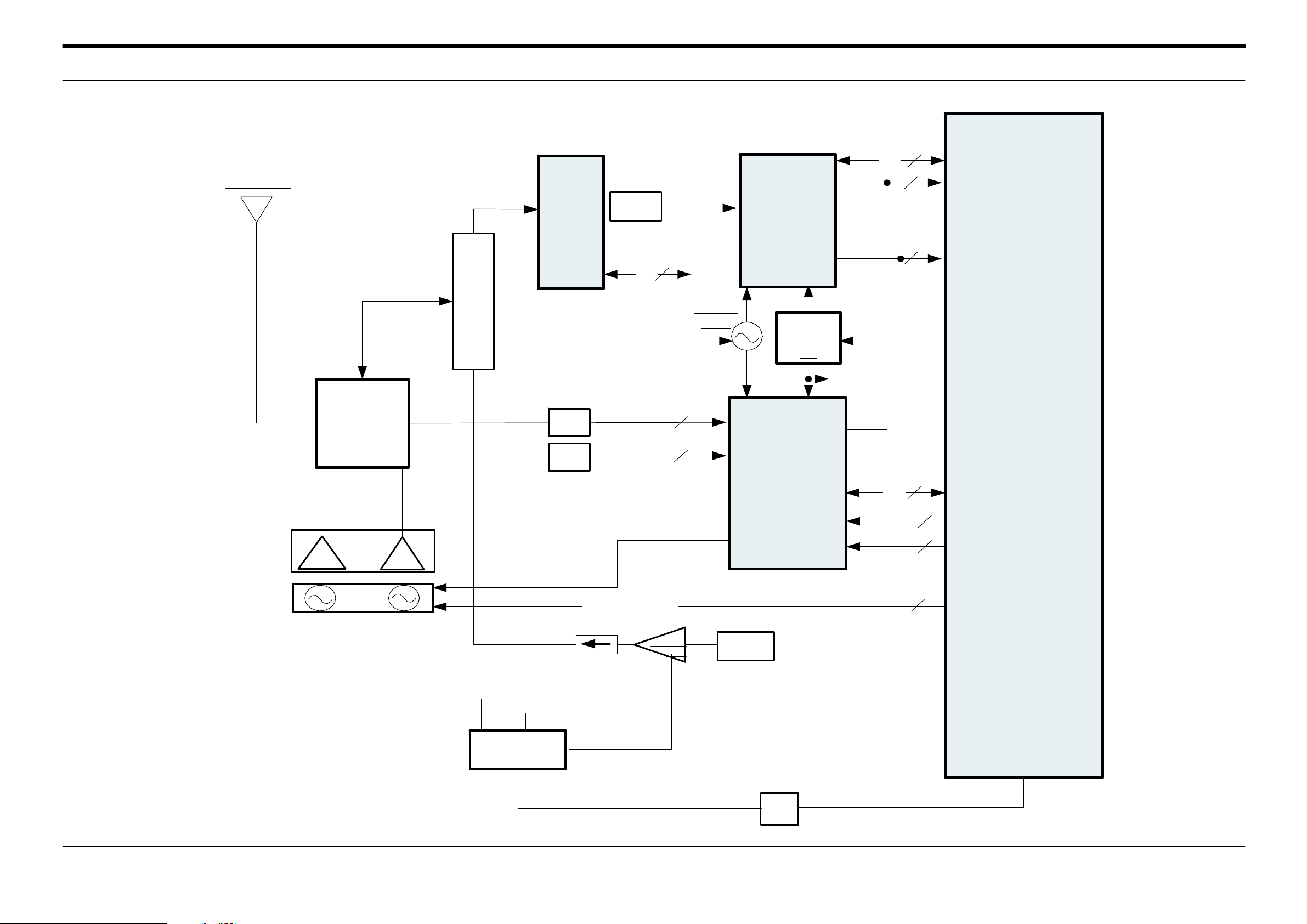
5. SGH-Z110V Block Diagrams
1. RF Solution Block Diagram
ANTENNA
D
U
P
L
E
X
E
R
RFL
6200
WCDMA
SAW
UMTS_RXP
UMTS_RXM
3
SBI
VCO_ BAND_SEL
(MSM_GPIO_INT41)
UCVA-
VCO
RFR620 0
TCXO
19.2M
Hz
RX_QP
RX_QM
RX_IP
RX_IM
TCXO
3
SBI
2
Q_IP/ Q_IM
2
I_IP/ I_I M
TRK_LO_AD J
GN060 11
(Switch
plexer)
RF5146
DUAL PAM
MQW-
DUAL VCO
DCSGSM
WPAM_ON(MSM)
VBATT
GSM
SAW
DCS
SAW
GSM_RXP
GSM_RXM
DCS_RXP
DCS_RXM
MOD_CP
DCS_VCO_EN/
GSM_VCO_EN
WCDMA
PAM
2
2
RTR6200
W_TX
SAW
VBATT_DCDC
RX_QP
RX_QM
RX_IP
RX_IM
TX_IP
TX_IM
TX_QP
TX_QM
SBI
MSM6200
3
2
I_OUT/ I_OU T_N
2
Q_OUT/ Q_OU T_N
2
GPIO_IN T22/ GPIO_I NT29
DC-
DC_Converter
5-1
SAMSUNG Proprietary-Contents may change without notice
This Document can not be used without Samsung's authorization
FDG
-
PA_R0
PA_RA NGE0
Page 25
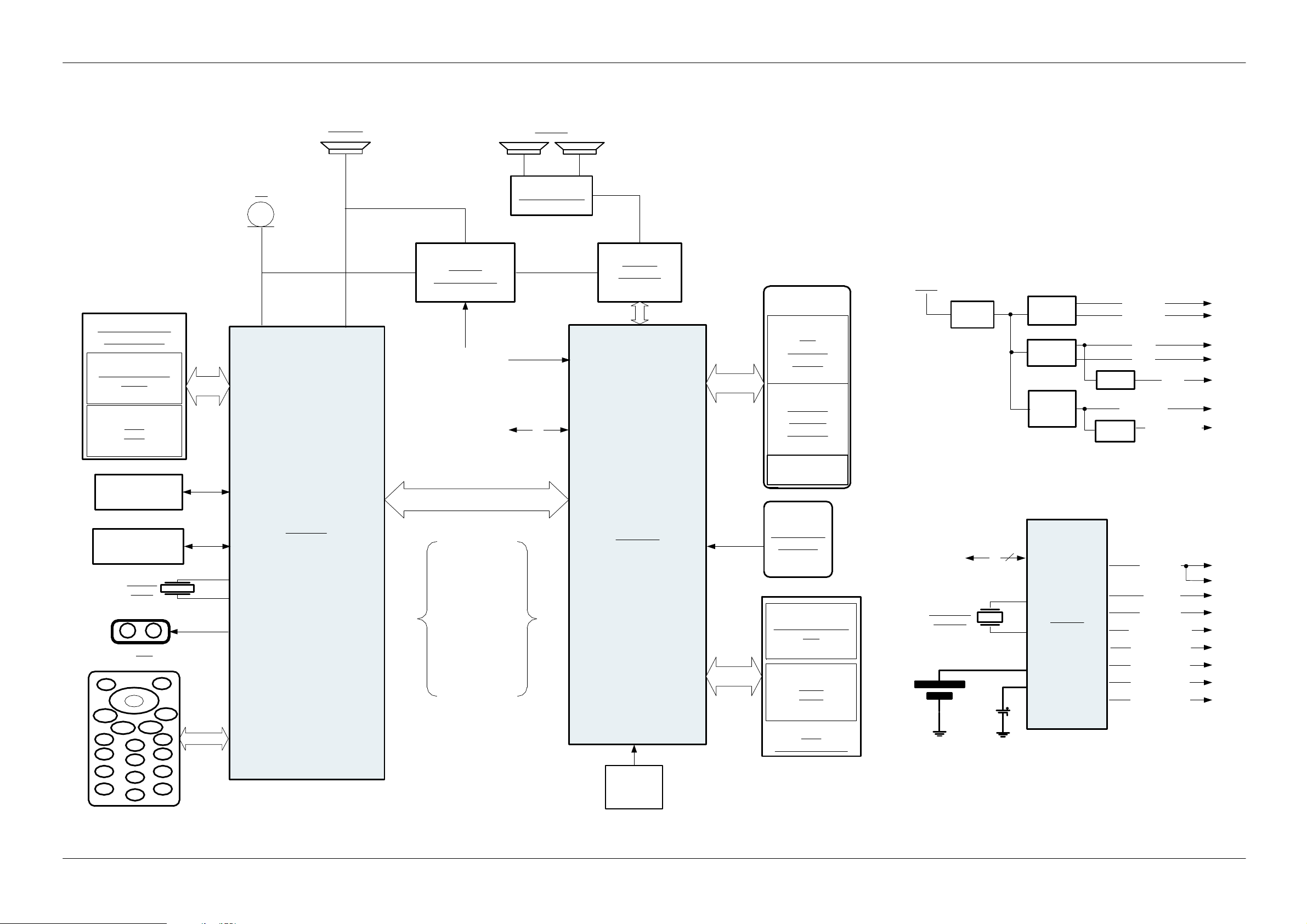
2. Base Band Solution Block Diagram
Block Diagrams
MCP(SPANSION)
(NOR+SRAM )
NOR FLASH MEMORY
128 Mbit
SRAM
32Mbit
MIC
RECEIVER
AK2442
Audio CODEC
I2C_SCL
I2C_CLK
SPEAKER
Audio Switchs
SBI
YMU769
Melody IC
(64 poly)
LCD
MODULE
Sub
TFT LCD
(96x96)
Main 2.2"
TFT LCD
(176x220)
VBATT
DC/DC
LDO
LDO2
LDO3
CAM(1.8VDV)
CAM(2.5VDV)
2.8VDV
2.8MLV
SW 2.8SLV
Maga(1.65VDV)
SW
Maga(1.65VDV_S)
...
TAL
1
4
7
*
USIM CARD
USB
USB CLK
48MHZ
IRDA
^
^
^
OK
^
CLR
MC
2
5
8
0
...
END
3
6
9
#
USB_XTAL_IN
USB_XTAL_OUT
MSM6200
EXT_INT_A
SLAVE
ASIC_STOP
EMG_A
AP_PWDN
HOST_IN_A
HCS
WR_N
RD_N
MSM --- AD(0:15)---Maga
HAD(0:15)
MSM---A(1:16)---Maga
HA(1:16)
MA55141
OSC
(19.2MHz)
CAMERA FLASH
1 Mega-pixel
CAMERA
NAND FLASH MEMORY
1Gbit
SDRAM
512Mbit
MCP
(NAND+SDRAM )
SLEEP XTAL
32.768kHz
MAIN
Battery
SBI
Backup
Battery
3
XTAR_IN
PM6050
XTAR_OUT
VCHARGER
COIN_CELL
VDD_P(2.8V)
VDD_LP(2.8V)
VDD_C(2.8)
VDD_A(2.6V)
VREG_BLUET(2.8V)
VREG_TCXO(2.8V)
VREG_SYNT(2.8V)
VREG_RFTX(2.8V)
VREG_RFRX(2.8V)
5-2
SAMSUNG Proprietary-Contents may change without notice
This Document can not be used without Samsung's authorization
Page 26
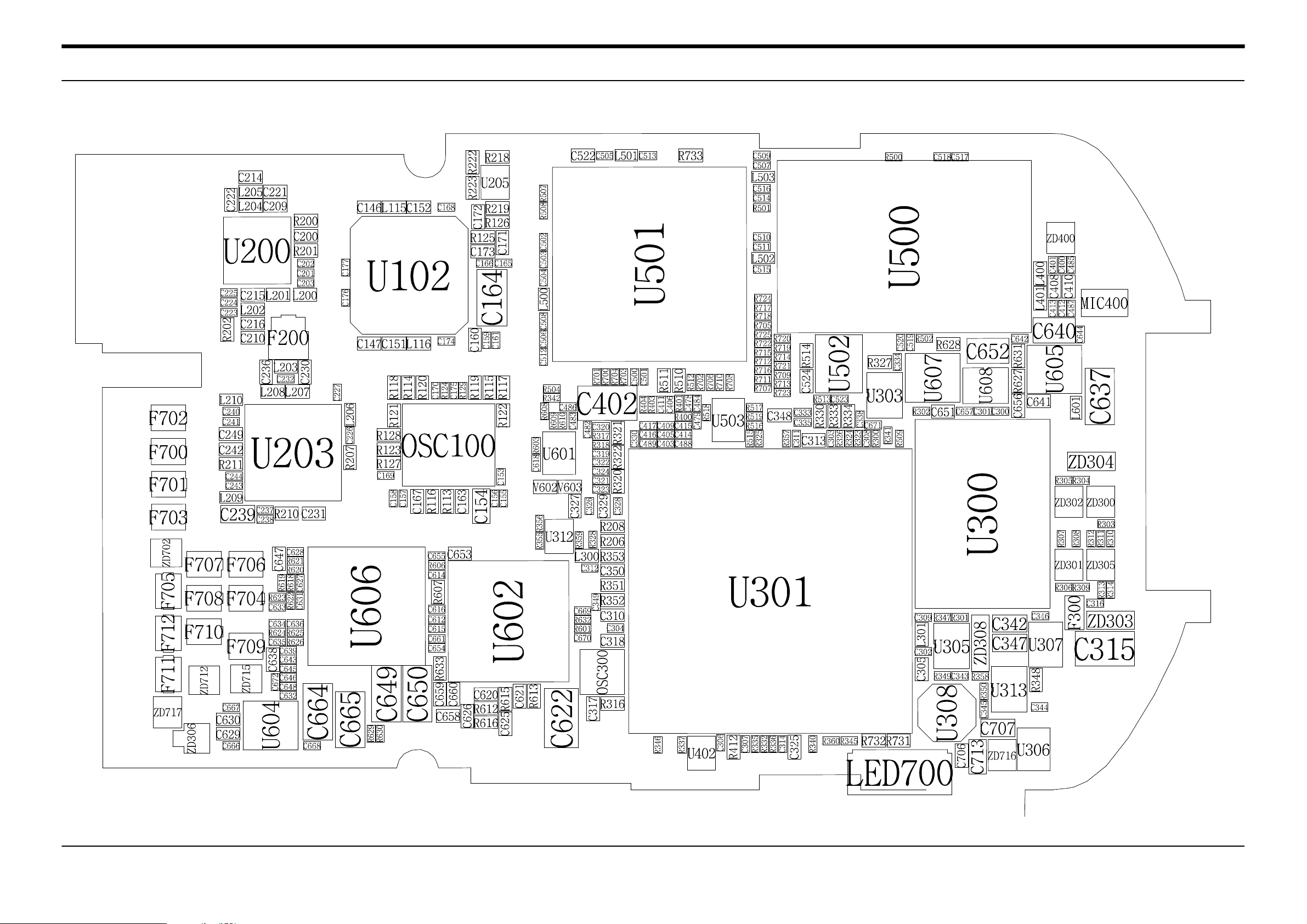
6. SGH-Z110V PCB Diagrams
1. Main PCB Top Diagram
6-1
SAMSUNG Proprietary-Contents may change without notice
This Document can not be used without Samsung's authorization
Page 27
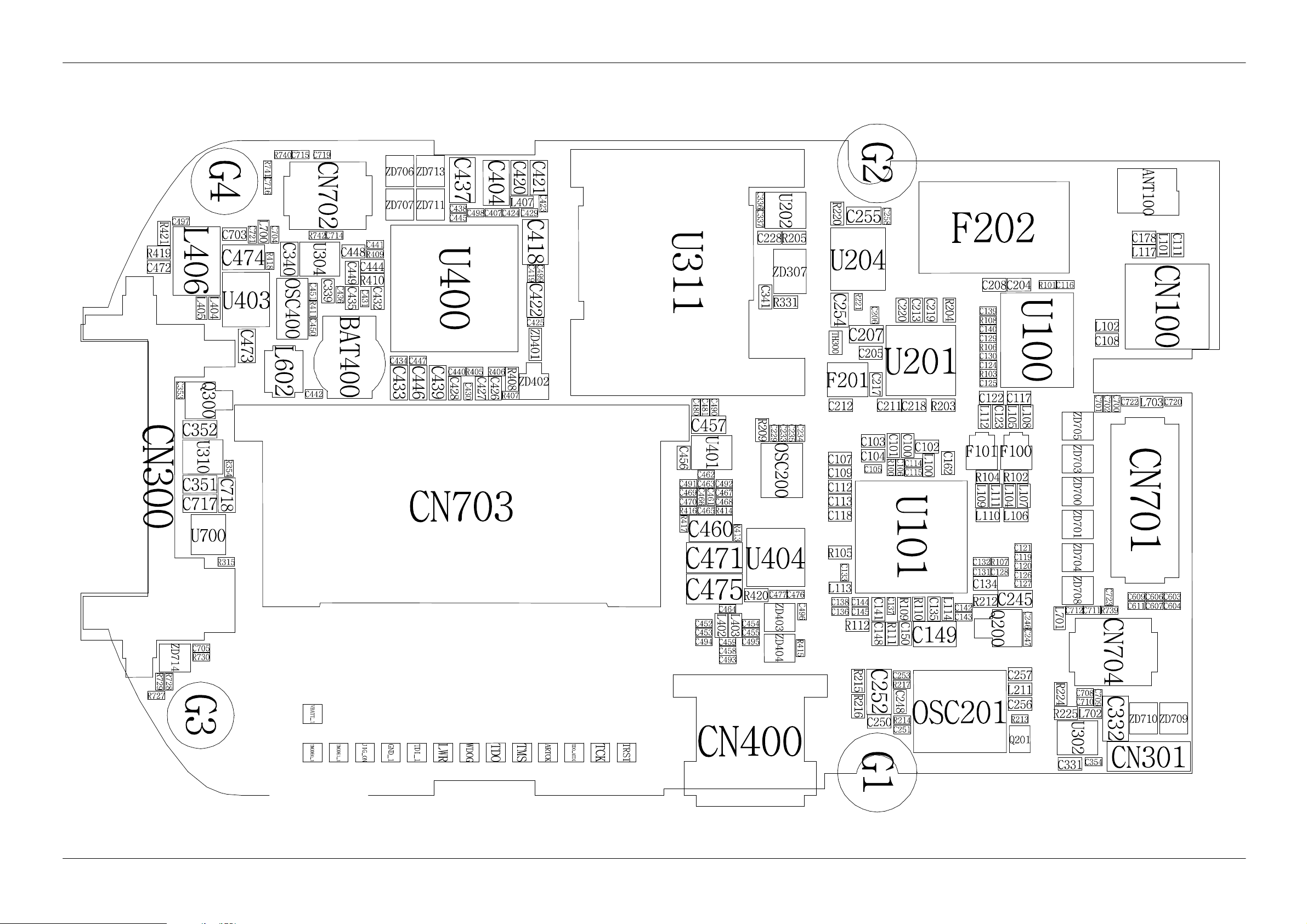
2. Main PCB Bottom Diagram
PCB Diagrams
6-2
SAMSUNG Proprietary-Contents may change without notice
This Document can not be used without Samsung's authorization
Page 28
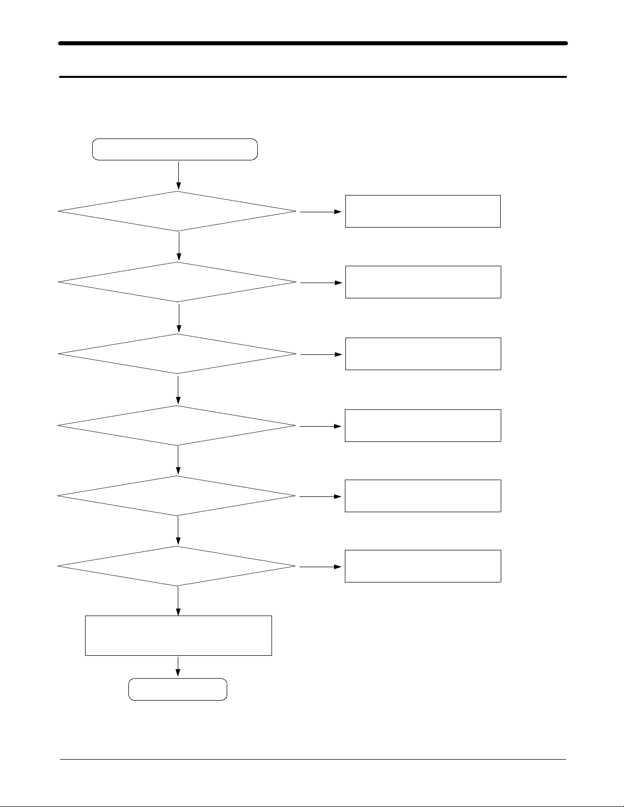
7. SGH-Z110V Flow Chart of Troubleshooting
1. Power On
' Power On ' does not work
Yes
Check the Battery Voltage
is more than 3.4V
Yes
U400PIN27(PS_HOLD)
= 2.8V?
Yes
Check the Clock at
R411=32.768KHZ
Yes
C421(VDD_C) = 2.8V? Check the PMIC
Yes
C420(VDD_P) 2.8V&
C425(VDD_A) = 2.6V?
No
Change the Battery
No
Check the PMIC related to PS_HOLD
No
Resolder OSC400
No
No
Check the PMIC
Yes
Check for the clock at
C448= 19.2MHz
Yes
Check the initial operation
Yes
END
SAMSUNG Proprietary-Contents may change without notice
This Document can not be used without Samsung's authorization
No
7-1
Check the clock generation circuit
(related to OSC200)
Page 29
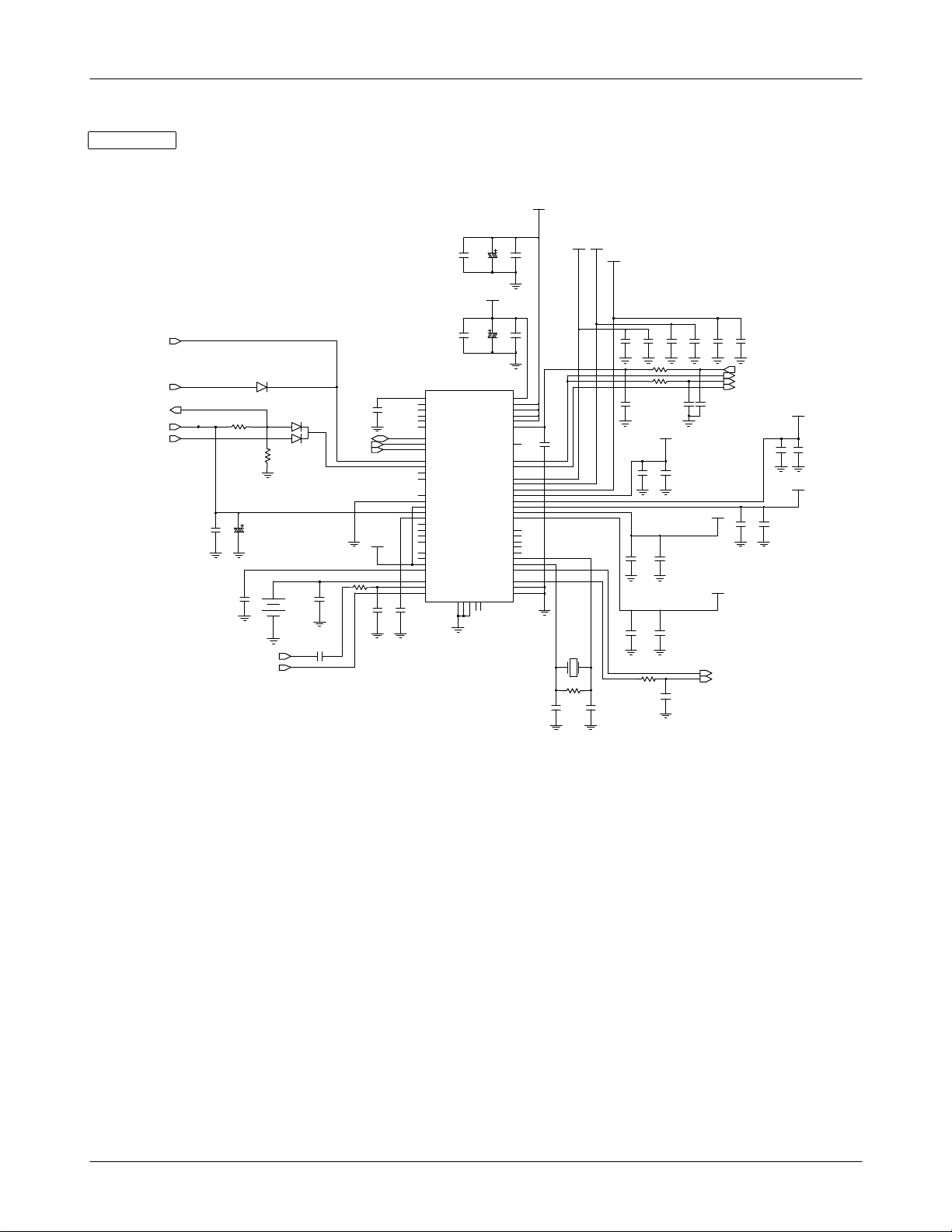
Flow Chart of Troubleshooting
VBATT
Power On
ON_SW
ZD401
ON_SW_SENSE_N
JIG_ON1
JIG_ON
PS_HOLD
JIG_ON
100nF
C438
SDB310 Q
22K R407
2
1
R408
33 K
C437
22UF
6.3V
BAT400
ML-414RM/F9HE
S
PO
TCXO
TCXO_EN
1
2
G
NE
C441
10pF
ZD402
DAN222TL
100PF
VDD_C
OSC400
C450
15pF
C430
100nF
VDD_P
VDD_A
C420
C421
C424
2.2UF
4.7UF
10pF
6.3V
6.3V
R405 100K
10K
R406
C426
C428
10NF
1UF
VREG_BT
C433
C434
2.2UF
10pF
6.3V
C439
C440
4.7UF
10pF
6.3V
C446
C447
2.2UF
10pF
6.3V
2
1
510 R410
R411
NC
C451
15pF
C449
NC
C423
10pF
C427
1UF
VREG_RFTX
VREG_RFRX
C422
4.7UF
6.3V
SLEEP_XTAL_I N
TCXO_OUT
C425
10pF
PMIC2_REF
RESET_F
RESET_N
PM_INT_N
C435
1UF
6.3V
10pF
C431
C436
10pF
VREG_SYNT
VREG_TCXO
6.3V
1U F
C43 2
C404
C498
22UF
27pF
6.3V
VBATT_PMI C
C418
C499
22UF
27pF
U400
PM6050-56BCCP-2C
43
ADC_BYP
40
PON_RESET/HKADC9
C429
41
HKADC8
100nF
42
HKADC7
44
HKADC6
45
100nF
HKADC5
31
SBDT
30
SBCK
29
SBST
32
KBDPWR_ON
27
PS_HOL D
33
CBLPWRON1
34
CBLPWRON0
56
CHG_CNTB
15
CHARGER_SEL
47
VDEF
1
VCHARGER
53
SPKR_BYP
50
SPKR_OUT/RINGER_OUT
52
SPKR_OUTB
48
SPKR_IN/RINGER_TONE
49
SPKR_INB
54
ICHARGEOUT
55
ICHARGE
2
VBAT
3
BAT_FETB
12
COIN_CELL
4
TCXO_I N
6
TCXO_EN
C445
NC
GND
GND
GND
61
62
58
59
60
3
SBDT
SBCK
SBST
VBATT
R409 0
C442
C444
NC
C448
1NF
6.3V
VDD_MSM
VDD_BT
VDD_RF
VDD_MAI N
VDD_DRV
REF_BYP
VBACKUP
PON_RESETB
MSM_INTERUPTB
VREG_MSM P
VREG_MSM C
VREG_MSMA
VREG_BLUET
VREG_SYNT
VREG_TCXO
VREG_RFTX
VREG_RFRX
KEYBD_DRV
GP2_DRV
GP1_DRV
LCD_DRV
VIBRATOR_DRV
XTAL_OUT
XTAL_I N
SLEEP_CLK
TCXO_OUT
REF_GND
NC
100nF
C407
100nF
C419
36
19
21
8
51
25
10
26
28
38
37
35
18
9
7
22
20
17
23
16
24
39
13
14
11
5
46
57
GND
FC-135 (0.032768MHz )
7-2
SAMSUNG Proprietary-Contents may change without notice
This Document can not be used without Samsung's authorization
Page 30
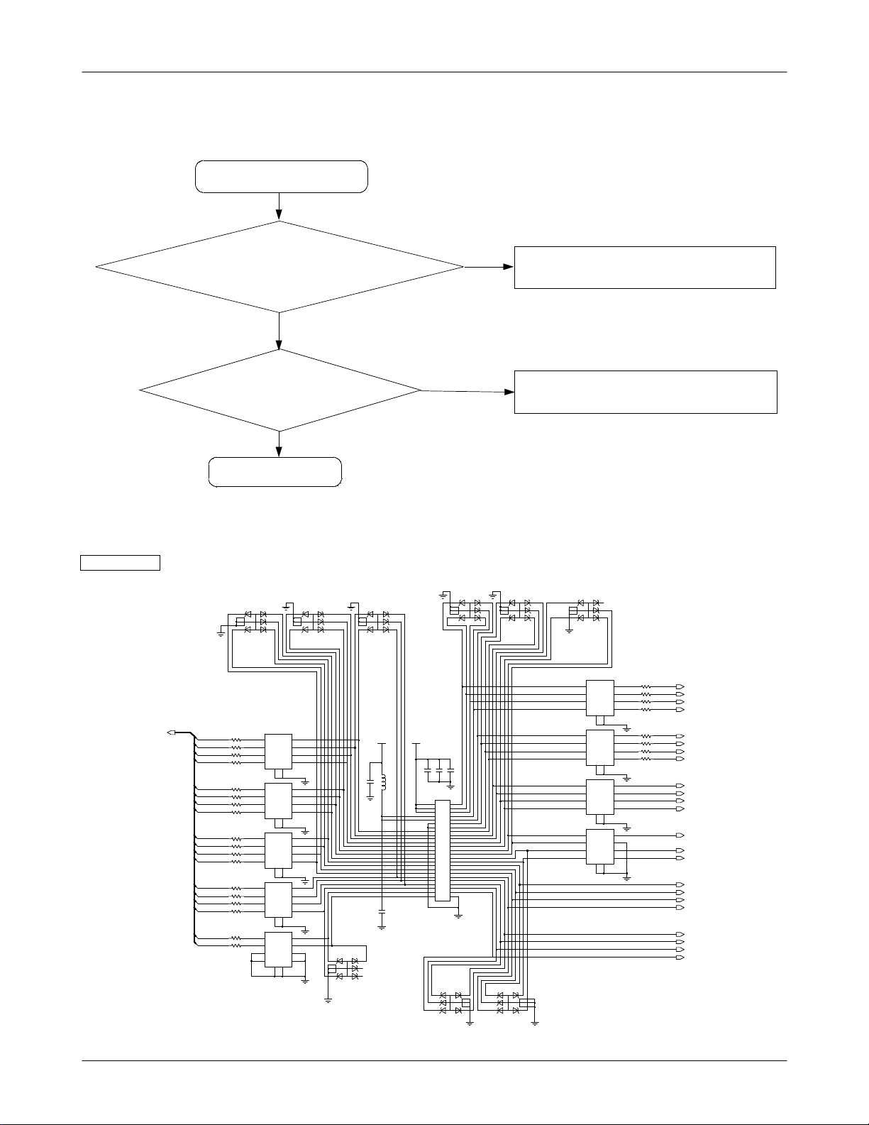
2. Initial
Flow Chart of Troubleshooting
Initial Failure
Yes
Initial
U400 (RESET_N) ="H"?
Yes
Is CN701 pin 46
(MLCD_RESET) OK?
Yes
END
ZD704
GMF05LC-HS3
1
7
2
8
3
ZD703
GMF05LC-HS3
6
5
4
6
1
7
5
2
8
4
3
1
7
2
8
3
ZD705
GMF05LC-HS3
No
Check the PMIC
No
Check the LCD RESET Circuit
ZD700
GMF05LC-HS 3
1
7
6
5
4
2
8
3
ZD701
6
5
4
6
1
7
2
5
8
4
3
ZD702
GMF05LC-HS3 GMF05LC-HS3
6
1
7
2
5
8
4
3
RGB(0:17)
RGB(17)
RGB(16)
RGB(15)
RGB(14)
RGB(13)
RGB(12)
RGB(11)
RGB(10)
RGB(9)
RGB(8)
RGB(7)
RGB(6)
RGB(5)
RGB(4)
RGB(3)
RGB(2)
RGB(1)
RGB(0)
F702
R705
R707 100
R711
R712 100
R715 100
R717 100
R718 100
R719 100
R720 100
R721
R722
R723
R725 100
OUT
100
IN
5
1
OUT
IN
6
2
OUT
IN
100 R709
100
100 R713
100 R714
100 R716
100
100
100
100 R724
7
3
IN
OUT
8
4
GG
9
10
F704
OUT
IN
5
1
OUT
IN
6
2
OUT
IN
7
3
OUT
IN
8
4
G
G
10
9
F706
OUT
IN
5
1
OUT
IN
6
2
OUT
IN
7
3
IN
OUT
8
4
GG
10
9
F707
OUT
IN
5
1
OUT
IN
6
2
OUT
IN
7
3
OUT
IN
8
4
G
G
91 0
F708
OUT
IN
5
1
OUT
IN
6
2
OUT
IN
7
3
IN
OUT
8
4
GG
9
10
1
7
2
8
3
GMF05LC-HS3
2.8VDV
VBATT
C701
C700
C702
33PF
47PF
27pF
C720
33PF
L703
BLM15HG102SN1D
CN701
50
1
50
1
49
2
49
2
48
3
48
3
47
4
47
4
46
5
46
5
45
6
45
6
44
7
44
7
43
8
43
8
42
9
42
9
41
10
41
10
40
11
40
11
39
12
39
12
38
13
38
13
37
14
37
14
36
15
15
36
35
16
35
16
34
17
34
17
33
18
33
18
32
19
32
19
31
20
31
20
30
21
30
21
29
22
29
22
28
23
28
23
27
24
27
24
26
25
26
25
C722
33PF
ZD708
6
5
4
14-5602-050-000-829
ZD71 0
GMF05LC-HS3
6
5
4
ZD709
GMF05LC-HS3
6
1
7
2
8
3
1
7
2
5
8
4
3
7-3
SAMSUNG Proprietary-Contents may change without notice
This Document can not be used without Samsung's authorization
F700
OUT
IN
5
OUT
6
OUT
7
OUT
8
F701
OUT
5
OUT
6
OUT
7
OUT
8
F703
OUT
5
OUT
6
OUT
7
OUT
8
F705
OUT
5
OUT
6
OUT
7
OUT
8
R700 100
1
IN
2
IN
3
IN
R703 100
4
G G
9
10
IN
1
IN
R706 100
2
IN
R708 100
3
IN
R710
4
G
G
9 10
IN
1
IN
2
IN
3
IN
4
G G
9
10
IN
1
IN
2
IN
3
IN
4
G
G
9 10
DCL K
100 R701
DSERI
100 R702
RGB_CLK
DEN
100 R704
MLCD_RESET
RGB_HSYNC
RGB_VSYNC
100
RGB_DE
SLCD_RS
SLCD_CS
SLCD_W R
SLCD_RESET
7_COLOR_EN
I2C_SCL
I2C_SDA
SPKL_P
SPKL_N
SPKR_P
SPKR_N
RCV_P
RCV_N
CAM_FLASH_EN0
CAM_FLASH_EN1
Page 31
Flow Chart of Troubleshooting
3. Sim Part
Phone can't access SIM Card
U311 pin 1,5 = "H"?
Yes
No
Check the SIM POWER
Yes
After Power ON,
Check USIM_CLK Signal on
U311 pin3 in a few second
Yes
After SIM card insert,
U311 pin 2 = "H(USIM_RESET)"?
Yes
Check the SIM Card
Yes
END
No
Check the 32k OSC
No
Replace PBA
7-4
SAMSUNG Proprietary-Contents may change without notice
This Document can not be used without Samsung's authorization
Page 32
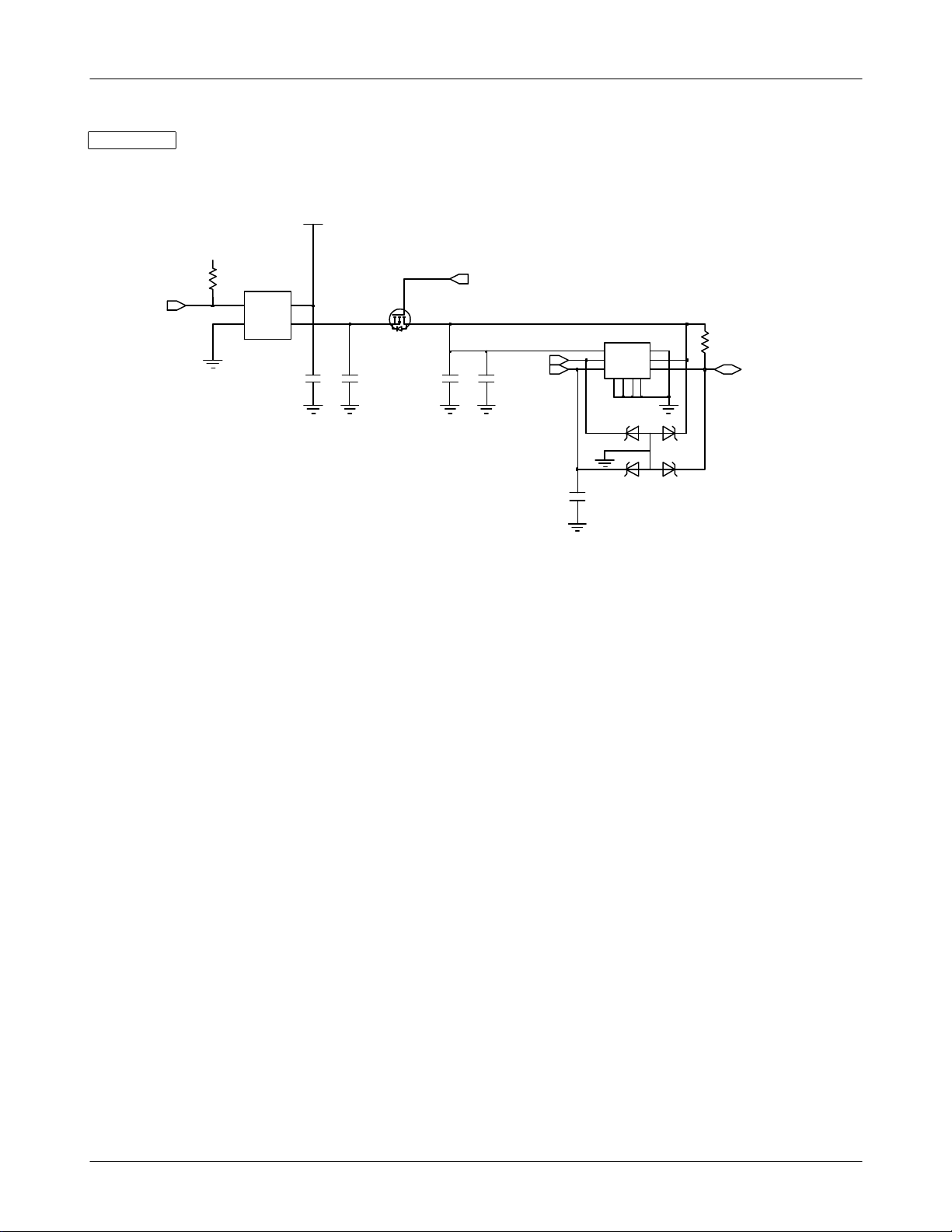
SIM
Flow Chart of Troubleshooting
VBATT
PS_HOLD
R354
10K
U310
1
CE
2
GND
R1180Q301B
VDD
VOUT
4
3
C351
4.7UF
C352
2.2UF
Q300
SI1305DL
2S
USIM_VCC_EN
1G
3D
USIM_RESET
C336
100nF
C337
10pF
USIM_CLK USIM_DATA
C341
27PF
1
2
3
U311
PC-D6-A3-H3.0- S
1
66
5
2
4
3
G G
G
7 G 8
9 10
ZD307
1
2
3
ESDALC6V1W5
R331
5
4
10K
5
4
7-5
SAMSUNG Proprietary-Contents may change without notice
This Document can not be used without Samsung's authorization
Page 33
Flow Chart of Troubleshooting
4. Speaker Part (Melody)
Speaker does not work
U602 pin6,28 = 2.8V?
Yes
No
Resolder or replace U605
Yes
Check the Clock signal at
Pin 2 of U602
(19.2MHz)
Yes
U602 pin 3 ≒ 2.8V?
(When U501 operate)
Yes
U602 pin 23
≒ Battery Volt ?
Yes
Is Speaker working?
No
Check the clock generation circuit
(related to U502 and U602)
No
Resolder U501
No
Check the circuit related to
"AMP1_IN/AMP2_IN" signal
No
Change the Speaker
Yes
END
7-6
SAMSUNG Proprietary-Contents may change without notice
This Document can not be used without Samsung's authorization
Page 34
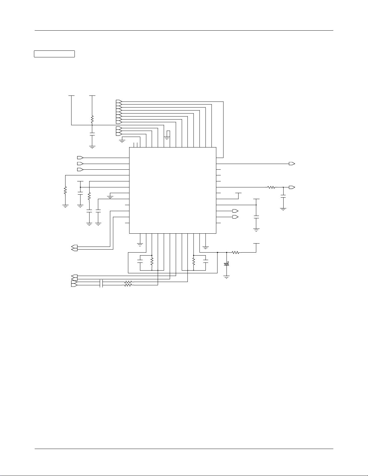
Speaker
Flow Chart of Troubleshooting
MEL_VCC
MEM_OE
LSI_CLK
MELODY_RESET
R606
0
SPKL_P
SPKL_N
MEL_R
MEL_L
AMP2_IN
AMP1_IN
C612
100nF
MEL_VCC
C614
1N F
C670
33PF
R601
0
2.8VD V
C615
100nF
R607
3.3K
MEMD(7)
MEMD(6)
MEMD(5)
MEMD(4)
MEMD(3)
MEMD(2)
MEMD(1)
MEMD(0)
MEMA(0)
MELODY_CS
MEM_WE
220NF C625
220NF C626
51
NC
1
_RD
2
CLKI
3
_RST
4
TESTI
5
PLLC
6
VDD
7
VSS
8
VREF
9
NC
10
SPOUT2-L
11
SPOUT1-L
12
NC
C620
10NF
R615 1K,1%
R616 1K,1%
13
50
NC
48
49
GND
L
SPVSS-
14
47
R
_W
L
SPVDD-
15
R612
46
45
D
A0
_CS
IOVD
U602
YMU769
L
L
EQ2-
EQ3-
17
16
2.7K
43
44
D0 D1
VSS
L
HPOUT-L/MONO
HPOUT-R
EQ1-
20
18
19
42
R
EQ1-
21
41 40
D2
R
EQ2-
22
R613
D3 D4
R
EQ3-
23
38
39
SPOUT2-R
SPOUT1-R
R
SPVDD-
24
2.7K
37
D5 D6
D7
_IRQ
PIO 0
PIO 1
PIO 2
LED
MT R
IOVDD
VDD
R
NC
SPVSS-
C621
10NF
36
35
34
MELODY_IRQ
33
32
31
MEL_VCC
30
29
MEL_VCC
R632
0
C669
33PF
MELODY_LED
28
27
26
25
C622
33U F
6.3V
SPKR_P
SPKR_N
0 R633
VBATT
C616
100nF
7-7
SAMSUNG Proprietary-Contents may change without notice
This Document can not be used without Samsung's authorization
Page 35
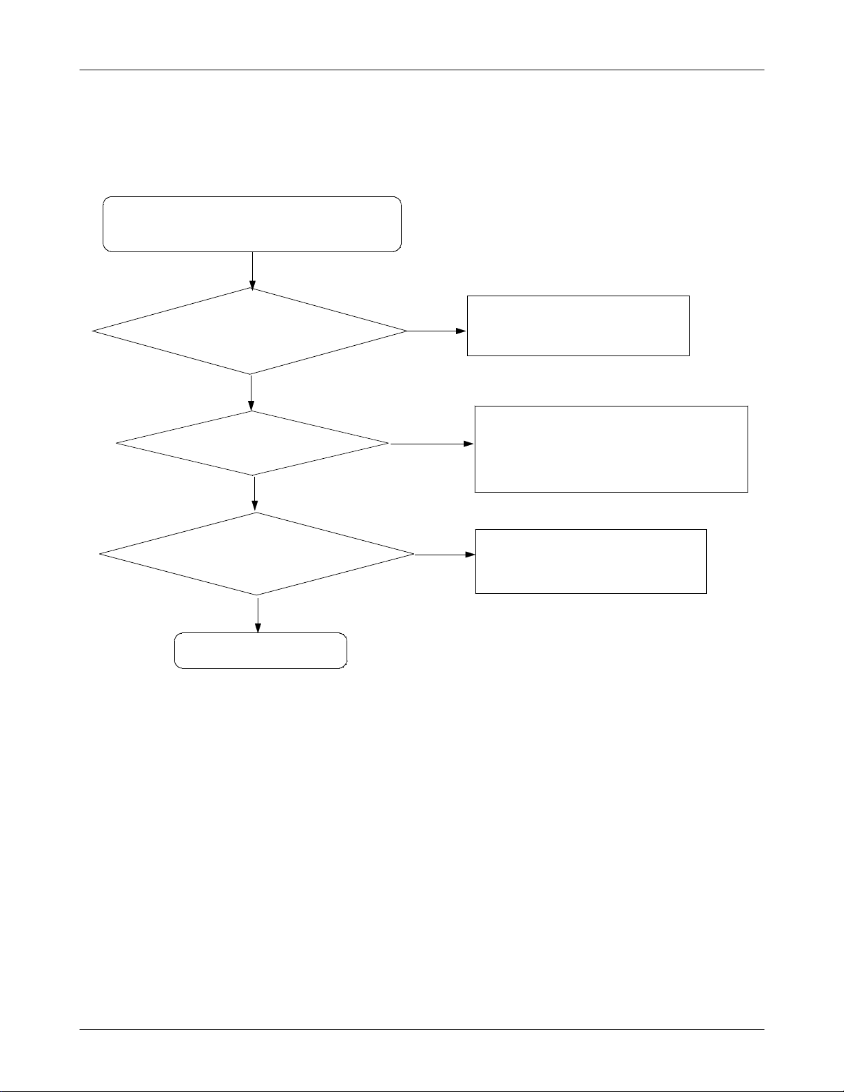
Flow Chart of Troubleshooting
5. Microphone part
Microphone does not work
Check the connection
from MIC
Yes
No
Resolder MIC
Yes
No
Check the circuit
from U301 to MIC
Yes
Check the MIC
Yes
END
Resolder the R400, R401, R403, R404,
L400, L401, C406, C411
No
Replace the MIC
7-8
SAMSUNG Proprietary-Contents may change without notice
This Document can not be used without Samsung's authorization
Page 36
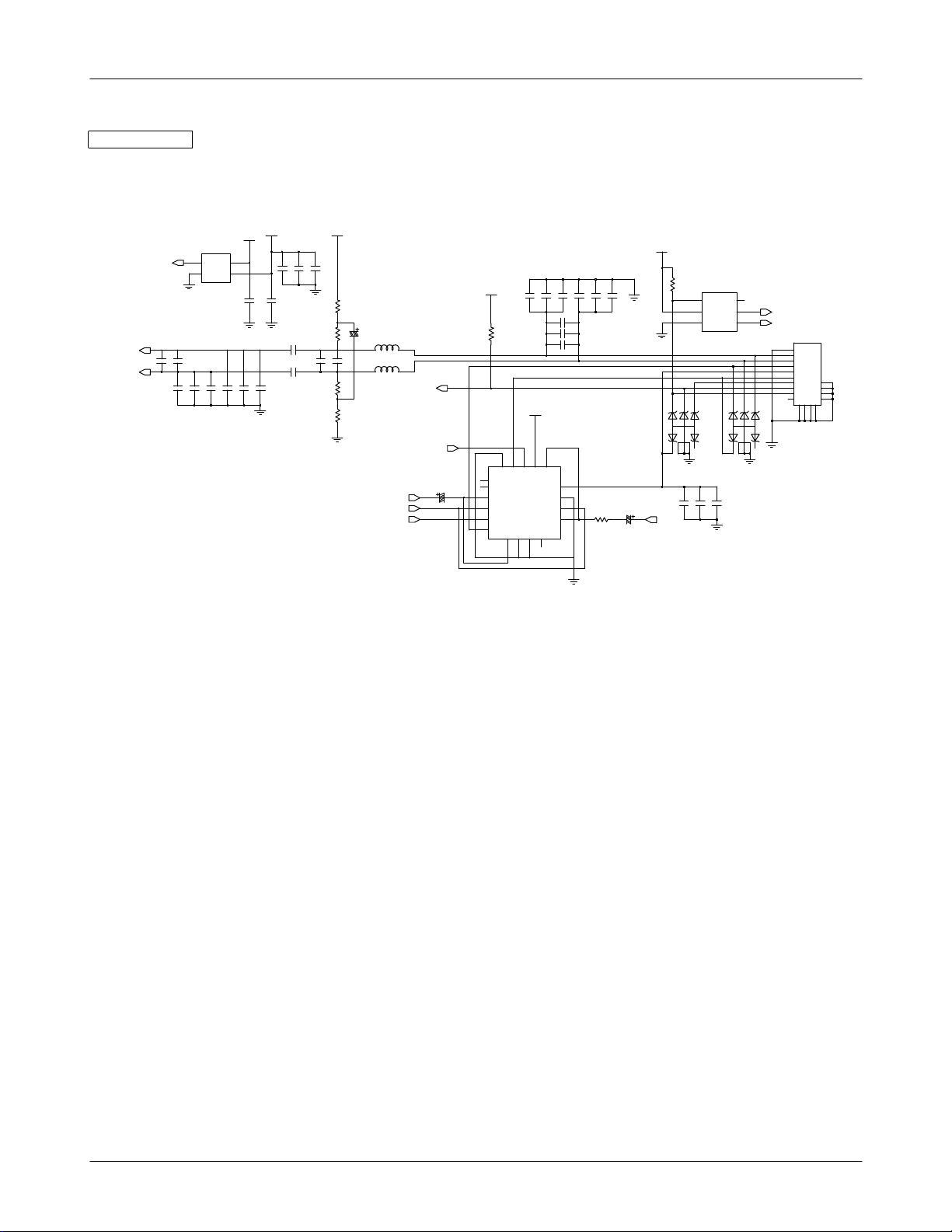
Microphone
Flow Chart of Troubleshooting
MIC2P
MIC2N
MIC_BIAS_ON
C462
15pF
100nF
100nF
MIC_BIAS
C481
C490
15pF
100nF
C455
C454
C453
C452
C494
9pF
27pF 27pF
EAR_L
C471
100UF
VDD_L P
R415
100K
VBATT
14
13 16
17
15
V+
D1
1S1
GND
21
NC
22
6.3V
NC
1
1S2
U404
STG3699AQTR
2
1-2I N
3
2S1
4
D2
GND
2S2
3S1
8
6
5
7
R413
1K
C460
R414
1.2K
C461
C465
33PF
C466
C464
NC
R416
1.2K
R417
1K
L402
33UF
BLM10B750SBPT
4V
L403
VOICE_AUDIO_MODE
BLM10B750SBPT
EAR1OP
JACK_I N
C458 15pF
C459 9pF
C493
4S2
D4
4S1
3-4I N
3S2
D3
15pF
9pF
15pF
NC
12
11
10
R420
16
9
VDD_LP
C495
C475
100UF
6.3V
EAR1ON EAR_R
R412
100K,1%
1
7
2
ZD403
GMF05LC-HS3
C476
9pF
U402
DG2011
1
6
IN
NO
5
2
COM
V+
3
GND
4 5 6
3
8
GMF05LC-HS3
C477
C496
15pF
NC
SCAN_5
4
NC
KEY_3
CN400
0-1674432- 1
1 1
22
3 3
44
5 5
66
15
7
7
G
16
88
G
17
9 9
G
10 10
18
G
G
GG
4 5 6
7
1
2
8
3
ZD404
G
11 12
13 14
MIC_BIAS
VBATT
U40 1
R1180Q181B-TR
1
CE
VDD
2
GND
VOUT
C463
9p F
C46 9
C467
C470
C491
27pF
15pF
15pF
9pF
C480
33PF
4
3
C45 6
C457
1UF
2.2UF
C468
C492
27pF
9pF
7-9
SAMSUNG Proprietary-Contents may change without notice
This Document can not be used without Samsung's authorization
Page 37
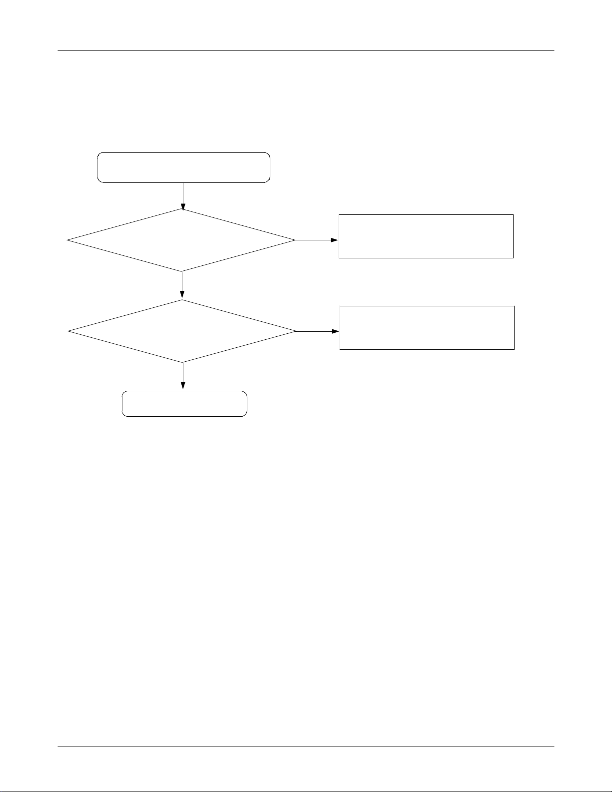
Flow Chart of Troubleshooting
6. Key Data Input
Check Initial Operation
Yes
When one of the keys is
When one of the keys is
pushed,
is it displayed on LCD?
Yes
pushed,
KEY_IO signal is OK?
Yes
END
No
Check the Dome sheet & Key Pad
No
Replace the PBA
7-10
SAMSUNG Proprietary-Contents may change without notice
This Document can not be used without Samsung's authorization
Page 38
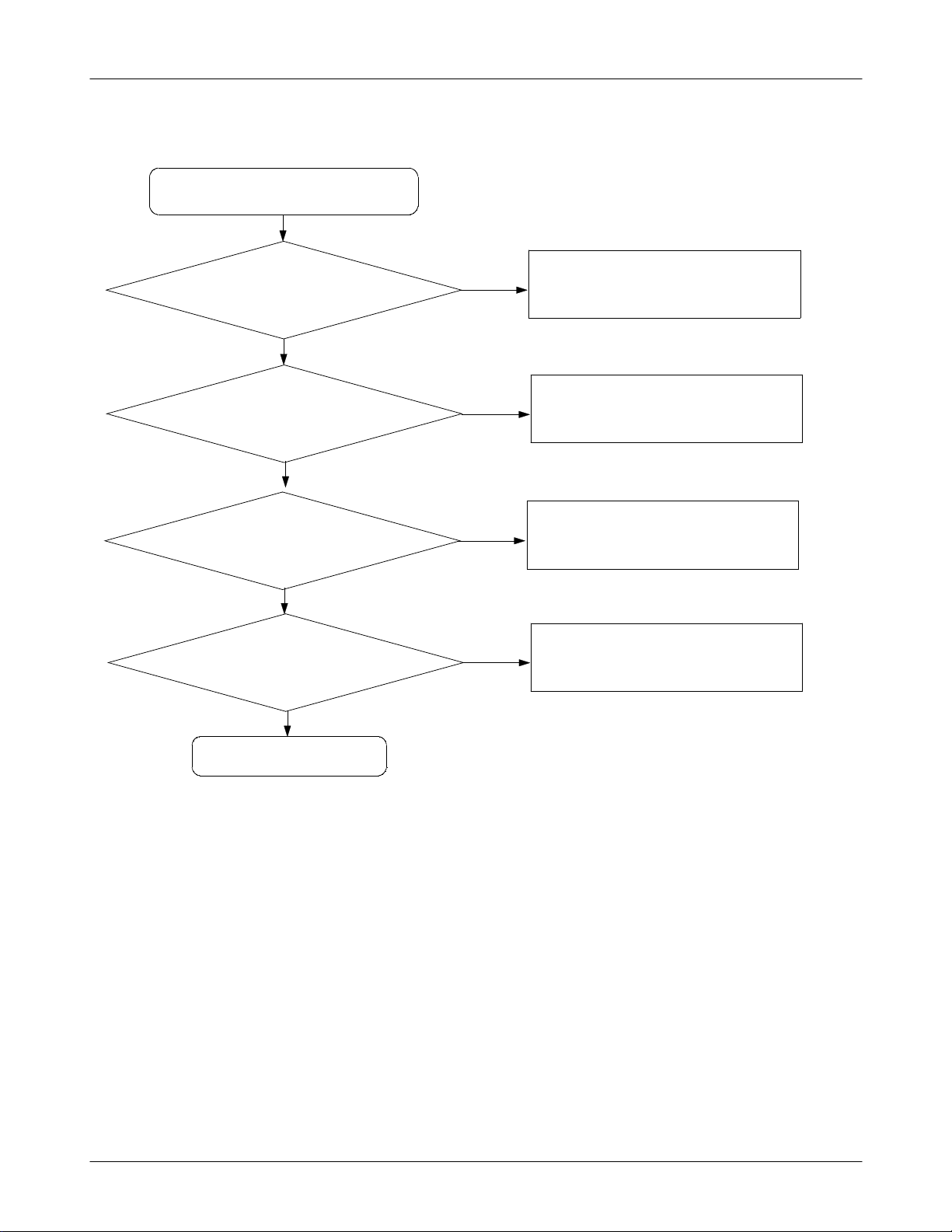
7. Receiver Part
Receiver does not work
U404 pin 2,10 = 2.8V?
C471, C475 = 1.2V?
Flow Chart of Troubleshooting
Yes
No
Resolder or replace U404
Yes
No
Resolder or replace C471, C475
Yes
Check the soldering of the
spaeaker wire
Yes
Is Receiver working?
Yes
END
No
Modufy the speaker wire soldering
No
Replace the Receiver
7-11
SAMSUNG Proprietary-Contents may change without notice
This Document can not be used without Samsung's authorization
Page 39
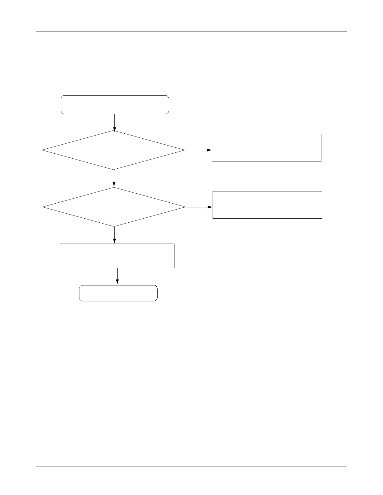
Flow Chart of Troubleshooting
8. Back Light (for Color Main LCD)
Backlight does not work
Yes
Is BACKLIGHT set
Always ON in the Menu?
Yes
When the volume key press,
Signal at R332, R335?
No
Set BACKLIGHT on AlwaysON
No
Replace or Resolder R332,R335
Yes
Replace the LCD Module
Yes
END
7-12
SAMSUNG Proprietary-Contents may change without notice
This Document can not be used without Samsung's authorization
Page 40
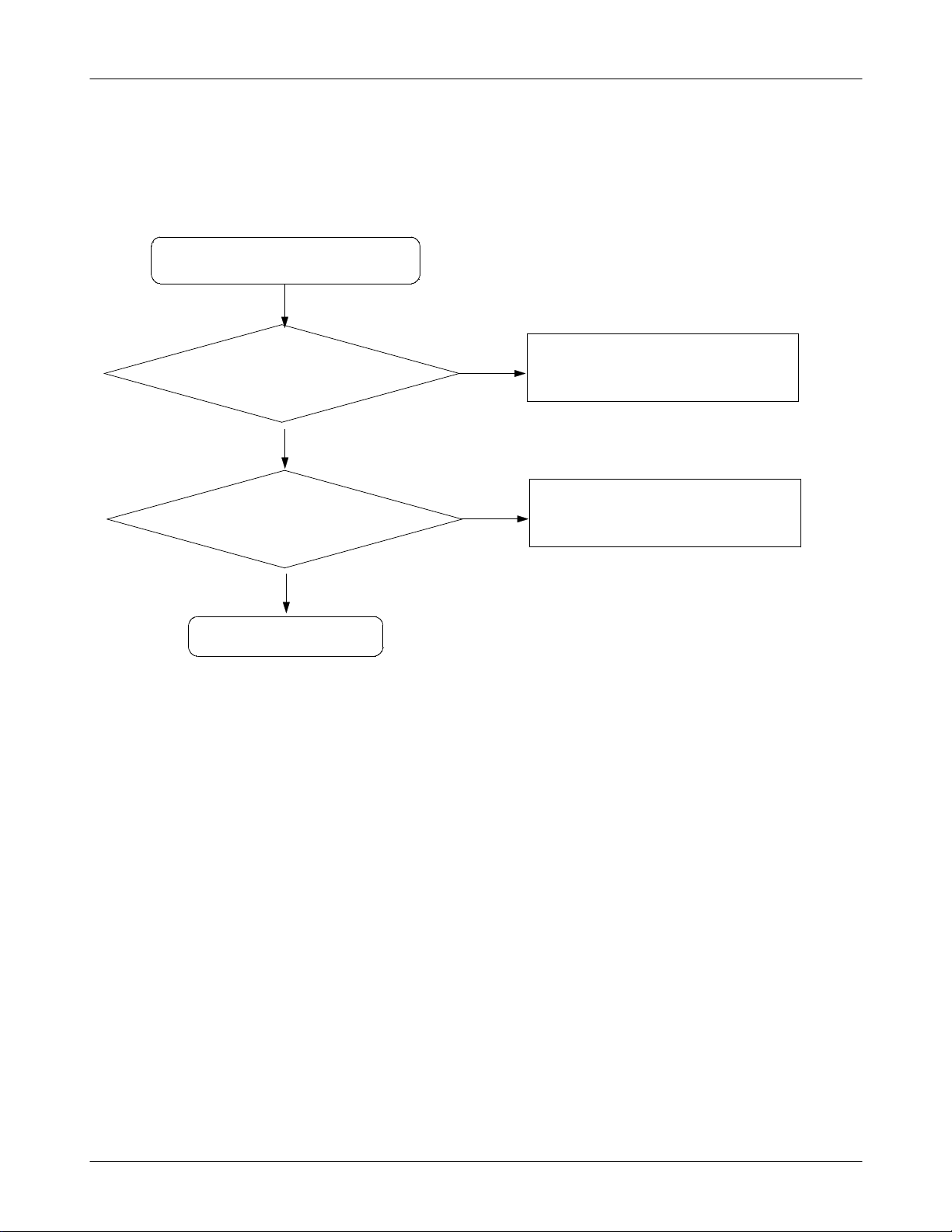
9. Key Back Light
Key Backlight does not work
Is BACKLIGHT set Always
ON in the Menu?
U304 pin 3 = "H"?
CN702 pin 15,17 = 3.3V?
Flow Chart of Troubleshooting
Yes
No
Set BACKLIGHT on AlwaysON
Yes
No
Resolder U302 / CN702 pin 30
or replace KeyPCB Module
END
Yes
7-13
SAMSUNG Proprietary-Contents may change without notice
This Document can not be used without Samsung's authorization
Page 41
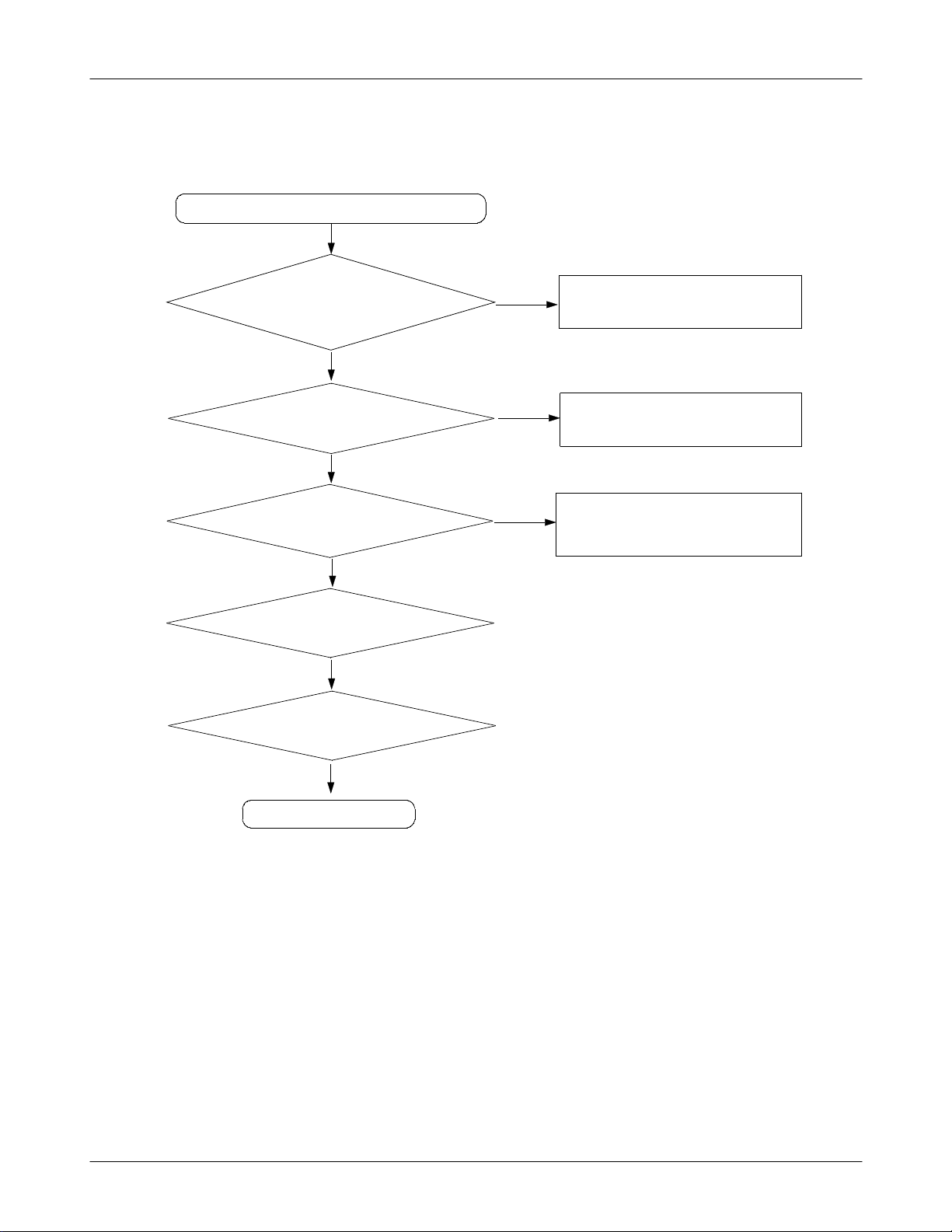
Flow Chart of Troubleshooting
10. Camera part
"Camera" function does not work
Yes
Check the Camera
connector on LCD module
Yes
CN704 pin 11,21 = 2.5V
pin 2, 20 = 1.8V
Yes
R733 = 34MHz?
Yes
Is there another problem?
Yes
Replace the camera
module
No
Connect the camera module
No
Replace or Resolder CN704
No
Replace or Resolder R733
END
7-14
SAMSUNG Proprietary-Contents may change without notice
This Document can not be used without Samsung's authorization
Page 42
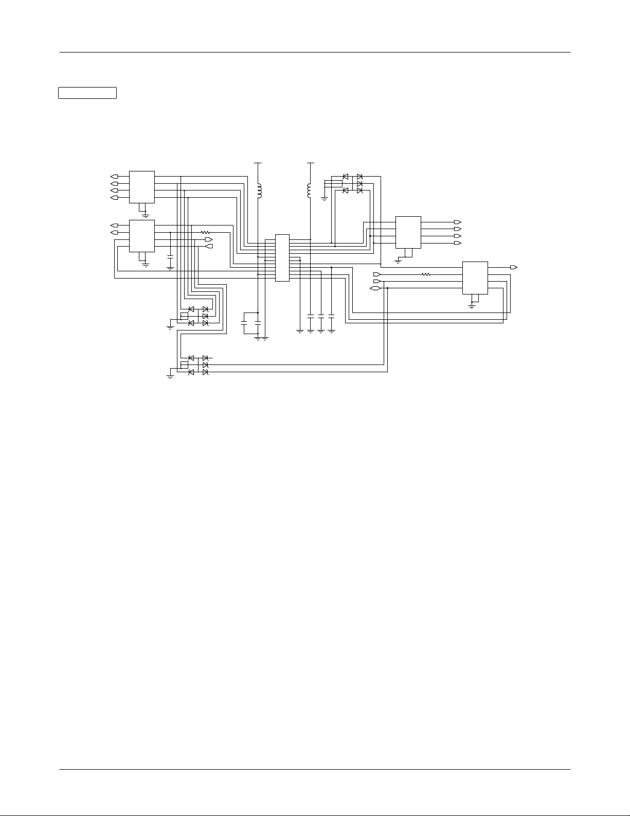
Camera
Flow Chart of Troubleshooting
CAM_DATA(7)
CAM_DATA(5)
CAM_DATA(3)
CAM_DATA(1)
CAM_VSYNC
CAM_PCLK
F709
OUT
IN
5
1
OUT
IN
6
2
OUT
IN
7
3
OUT
IN
8
4
G
G
9 10
F711
OUT
IN
5
1
OUT
IN
6
2
OUT
IN
7
3
OUT
IN
8
4
G G
9
10
C723
NC
R739 0
ZD715
GMF05LC-HS3
1
7
2
8
3
ZD717
GMF05LC-HS3
1
7
2
8
3
*R739-Close to connecto r
M_I2C_SCL
CAM_SLEEP
6
5
4
6
5
4
2.5VDV
L701
BLM15HG102SN1D
14-5602-024-000-829
1
3
5
7
9
11
13
15
17
19
21
23
C711
C712
47PF
100nF
1.8VDV
L702
BLM15HG102SN1D
CN704
22
1
4
3
4
6
5
6
8
7
8
10
9
10
12
11
12
13
14 14
16
15
16
18
17
18
20
19
20
22
21
22
24 24
23
C710
100nF
ZD712
GMF05LC-HS3
6
1
7
2
5
8
4
3
F710
OUT
IN
5
1
OUT
IN
6
2
OUT
IN
7
3
IN
OUT
8
4
GG
9
10
CAM_CLK
CAM_RESET
M_I2C_SDA
C708
C709
33PF
27pF
*R733-Close to Megachi p
CAM_DATA(6)
CAM_DATA(4)
CAM_DATA(2)
CAM_DATA(0)
F712
OUT
IN
5
1
47 R733
OUT
IN
2
OUT
IN
3
OUT
IN
4
G
G
91 0
CAM_HSYNC
6
7
8
7-15
SAMSUNG Proprietary-Contents may change without notice
This Document can not be used without Samsung's authorization
Page 43
11. GSM Receiver
Flow Chart of Troubleshooting
RF input : CH center freq : 442.6MHz
RX ON
Amp : -50dBm
Yes
C117
>= -60dBm
Yes
L106
>= -65dBm
Yes
Resolder U101
END
No
Resolder U100
No
Resolder F100
7-16
SAMSUNG Proprietary-Contents may change without notice
This Document can not be used without Samsung's authorization
Page 44
Flow Chart of Troubleshooting
12. GSM Transmitter
TX ON (5Level)
Yes
OSC100 pin10
<= 3.5V
Yes
OSC100 pin1
>= 2dBm
Yes
L115
>= 30dBm
Yes
C108
>= 30dBm
No
Check U100
No
No
No
Resolder U101
Resolder OSC100
Resolder U102
END
7-17
SAMSUNG Proprietary-Contents may change without notice
This Document can not be used without Samsung's authorization
Page 45
13. DCS Receiver
Flow Chart of Troubleshooting
RF input : CH center freq : 1842.8MHz
RX ON
Amp : -50dBm
Yes
C122
>= -60dBm
Yes
L110
>= -65dBm
Yes
Resolder U101
Yes
END
No
Resolder U100
No
Resolder F101
7-18
SAMSUNG Proprietary-Contents may change without notice
This Document can not be used without Samsung's authorization
Page 46
Flow Chart of Troubleshooting
14. DCS Transmitter
TX ON (0Level)
YES
OSC100 pin10
<= 3.5V
Yes
OSC100 pin5
>= 2dBm
Yes
C151
>= 25dBm
Yes
C108
>= 25dBm
No
Check U100
No
No
No
Check U101
Check OSC100
Check U102
END
7-19
SAMSUNG Proprietary-Contents may change without notice
This Document can not be used without Samsung's authorization
Page 47
15. WCDMA Receiver
Flow Chart of Troubleshooting
RF input : CH center : 10700 ch
RX ON
Amp : -50dBm
Yes
C208
>= -55dBm
Yes
C214
>= -60dBm
Yes
L202
>= -70dBm
Yes
C203
>= -75dBm
No
No
No
No
Check & Resolder U100
Resolder F202
Check & Resolder U200
Resolder F200
Yes
C231
19.2MHz
Yes
L206,L209,L210
=2.8V?
Yes
Check U203
Yes
END
No
No
Check & Resolder OSC200
Check U400
7-20
SAMSUNG Proprietary-Contents may change without notice
This Document can not be used without Samsung's authorization
Page 48
Flow Chart of Troubleshooting
16. WCDMA Transmitter
TX ON (PDM for 23dBm)
Yes
C212
>= -5dBm
Yes
C211
>= -5Bm
Yes
C213
>= 20dBm
Yes
C208
>= 20dBm
Yes
C108
>= 20dBm
No
No
No
No
Check & Resolder U101
Check & Resolder F201
Resolder U201
Check & Resolder F202
No
Check U100
END
7-21
SAMSUNG Proprietary-Contents may change without notice
This Document can not be used without Samsung's authorization
Page 49
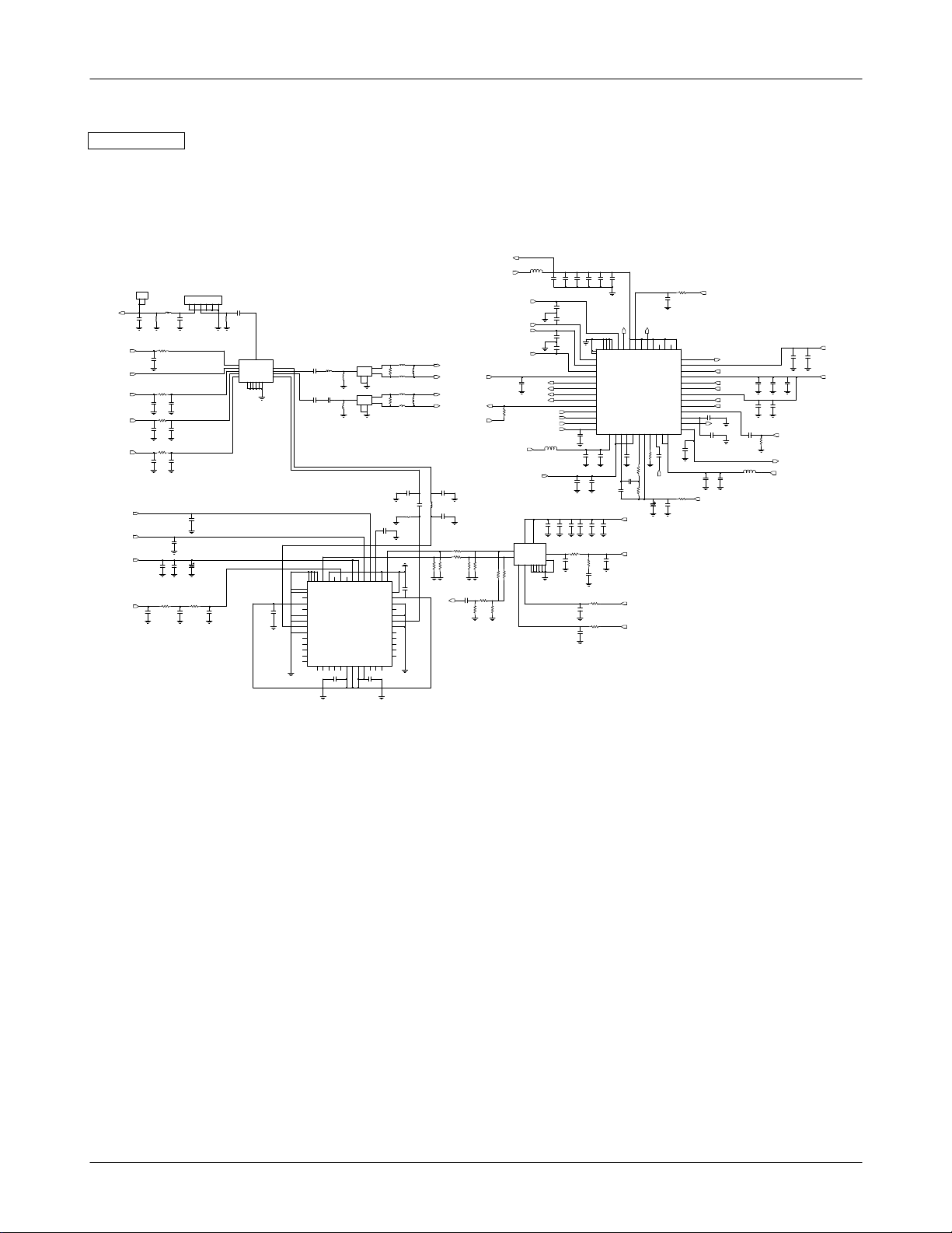
Transmitter
ANT100
-
1
2
1
2
AN T
L117
C178
1.2PF
15nH
R101 10
VREG_RFRX
C116
1NF
UMTS_ANT
R103
GSM_BAN D
1K
C124
33PF
R106
1K
C129
33PF
R108
1K
C139
33PF
VBATT
C165
100nF
R126
10K,1%
C172
330PF
GSM_ANT_SEL2_N
GSM_ANT_SEL1_N
GSM_ANT_SEL0_N
GSM_PA_PWR_SV
GSM_PA_PWR_CTL
Flow Chart of Troubleshooting
VREG_RTR
L100
BLM15HG102SN1D
VREG_RFTX
CN100
KMS-158
G
G G
A C
G
4 5
6
2
3
1
L101
3.3nH
C111
NC
C125
33PF
C130
33PF
C140
33PF
C159
10nF
C161
10nF
C166
47PF
C171
180PF
C108
33PF
L102
33nH
U100
GN06011L01SA
3
ANT
VD D
6
GSM-TX
UMTS
9
16
GSM-RX
IN_A
15
IN_B
DCS-RX
14
IN_C
DCS-TX
GG
G
G
GG
10 12
24
78
C164
100UF
6.3V
R125
8.2K
C173
1.2PF
C174
1NF
C117
L105
39PF
1
5
11
13
9
11
52
53
54
1
3
4
5
6
7
8
10
12
51
GND
GN D
GN D
NC
2
VCC2GSM
NC
GN D
GN D
GSM850/900OUT
GN D
NC
NC
NC
NC
NC
4.7nH
L108
NC
C123
C122
39PF
39PF
L112
10nH
46
45
48
47
44
49
50
M
M
NC
GND GND
GND
VRAMP
VCC1GS
GND1GS
GSM850/900IN
U102
RF5146
M
VCC3GS
NC
NC
NC
NC
NC
19
14
15
16
17 22
13
100PF C176
L104
10nH
F100
B7837
3
OUT
1
R102
IN
4
NC
GG
OUT
2
5
F101
B7844
3
OUT
1
R104
IN
4
NC
GG
OUT
2
5
C160
1NF
37
41
39
40
42 43
38
T
T
NC
VBAT
VBAT
36
BANDSEL
TXENABLE
NC
DCS/PCSIN
VCC1DCS/PCS
35
VCC2DCS/PCS
34
GN D
33
NC
32
GN D
31
DCS/PCSOUT
30
GN D
29
NC
28
NC
27
NC
26
NC
25
NC
VCC3DCS/PCS
VCCOUT
VCCOUT
NC NC
NC
21 18
20
24
23
C177
10nF
GSM_RXP
L106
L107
18nH
10nH
GSM_RXM
L109
2.2nH
L110
L111
5.6nH
2.2nH
C147
0.75PF
C151
2PF
L116
6.8nH
C168
1N F
VREG_RTR
DCS_RXP
DCS_RXM
SYNTH_LOCK
C146
2PF
L115
8.2nH
C152
NC
R114 30
R115
30
R117
R118
R119
180
180
180
C169
33PF
TXVCO
TX_Q P
TX_Q M
TX_I P
TX_IM
C118
100NF
R105
10K
VDD_P
VDD_ P
OSC100
MQW510C869M
12
2
VB
5
OUT1
1
OUT2
SW 1S W2
R120
2
4
180
R122
R121
68
120
R123
100
R127
R128
82
82
VREG_BT
3 G 6
8
GG
1
VB
7
RX_Q P
RX_Q M
RX_I P
RX_I M
RF_ON_TX_ON
BLM15HG102SN1D
VC
G
G
G
G
11 9
13
C102
C103
C101
C100
100N F
C107
150PF
C109
150PF
C112
150PF
C113
150PF
SBCK
SBD T
SBST
L113
C153
C157
33PF
100nF
10
14
C105
C104
33PF
1N F
10NF
10pF
15PF
R100
1K
TX_AGC_AD J
C106
4.7nF
F
UMTS_TXRF
DAC_RE
49
48
50 51
47
P
GND
GND
GND
GND
TX_Q
VDDM
VDDA
CP1
14
15 18 22
16
C148
270PF
C156
10nF
C162
1.5NF
45
46
F
A
VDD
DAC_RE
U101
RTR6200-48BCCP
VDDA VDDA
CP_HOLD1
19
17
C137
10nF
R109
3.3K
C141
2.7N F
R111
10K
VREG_RFTX
MOD_CP
DCS_VCO_EN_N
GSM_VCO_EN_N
L
VCONTRO
38
40
42 44
43
39
41
A
A
A
A
C
C
DN
DN
VDD
VDD
VDD
VDD
37
TX_MOD_CP
UMTS_OUT
VDD A
TX_VCO_I N
VDD A
DCS_INP
DCS_INN
VDD A
EGSM_INP
EGSM_INN
PLL2_VCO_I N
CP_HOLD2
FAQ 2
VDDA
VDDA
R_BIAS
TCXO
FAQ1
20
23
24
21
C135
1NF
R110
11.3K,1%
TCXO
C149
C150
10UF
33PF
6.3V
MOD_CP
36
35
TXVCO
34
33
32
31
30
29
28
27
10nF C128
26
FAQ2
25
C131
CP2
27pF
C134
39PF
C142
C143
33P F
1N F
R112
10
VREG_BT
DCS_RXP
DCS_RXM
GSM_RXP
GSM_RXM
C120
33PF
C126
33PF
C132
27p F
L114
BLM15HG102SN1D
C119
100nF
1N F
C127
100nF
R107
100
VREG_SYN T
C121
RX_VCO
CP2
VREG_RTR
C114
C115
33P F
100nF
VREG_RTR
52
53
NC
54
NC
1
TX_Q N
2
TX_IP
3
TX_IN
4
VDDA
5
RX_Q P
6
RX_Q N
7
RX_I P
8
RX_I N
9
LOCK
10
SBCK
11
SBD T
12
SBST
13
RF_O N
C133
100PF
C136
C138
100nF
33PF
C144
C145
33PF
100nF
C154
C155
C158
4.7UF
1N F
15pF
R113
82
C163
120PF
R116
39
C167
22NF
R124
100
C170
15pF
R129
100
C175
15pF
7-22
SAMSUNG Proprietary-Contents may change without notice
This Document can not be used without Samsung's authorization
 Loading...