

SAMSUNG Z510 Service Manual
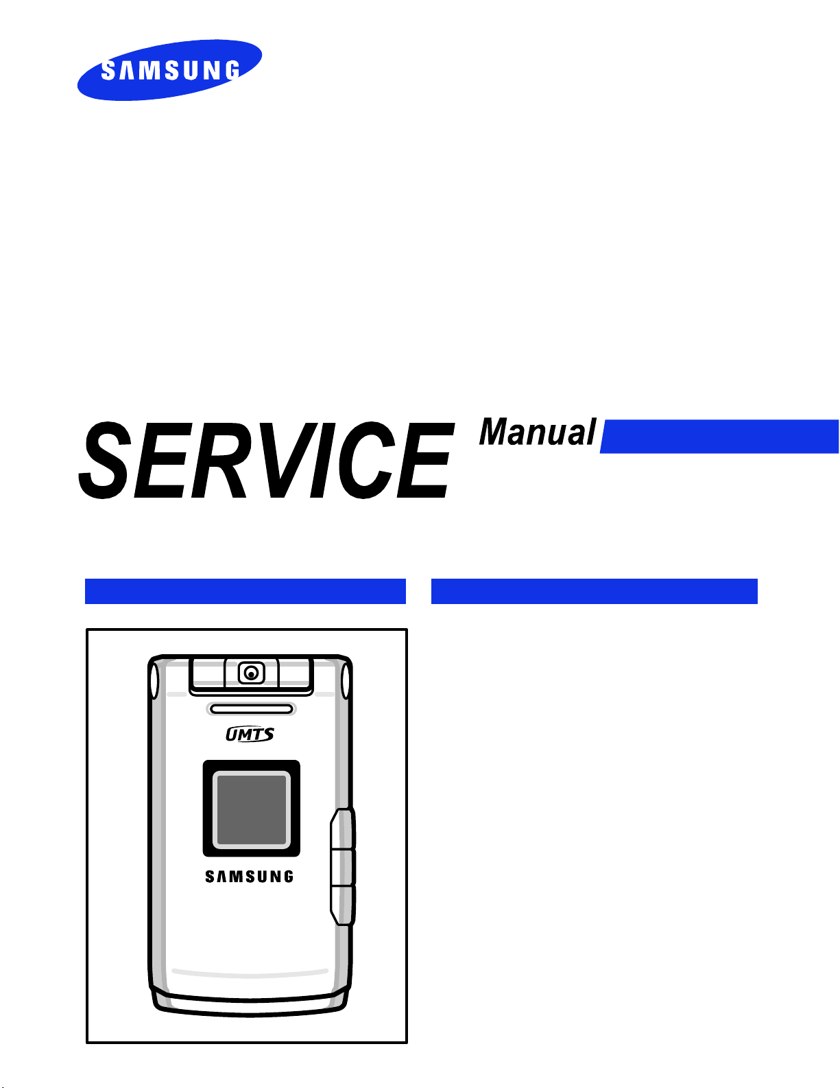
UMTS TELEPHONE
SGH-Z510
UMTS TELEPHONE
CONTENTS
1. Specification
2. Flow Chart of Troubleshooting
3. Exploded Views and Parts List
4. Electrical Parts List
5. PCB Diagrams
6. Block Diagrams

1. SGH-Z510 Specification
1-1. UMTS General Specification
GSM900
Phase 1
Freq. Band[MHz]
Uplink/Downlink
ARFCN range 1~124
Tx/Rx spacing 45MHz 45MHz 95MHz 80MHz 190MHz
Mod. Bit rate/
Bit Period
Time Slot
Period/Frame
Period
Modulation 0.3GMSK 0.3GMSK 0.3GMSK 0.3GMSK QPSK
MS Power 33dBm~13dBm 33dBm~5dBm 30dBm~0dBm 30dBm~0dBm
890~915
935~960
270.833kbps
3.692us
576.9us
4.615ms
EGSM 900
Phase 2
880~915
925~960
0~124 &
975~1023
270.833kbps
3.692us
576.9us
4.615ms
DCS1800
Phase 1
1710~1785
1805~1880
512~885 512~810
270.833kbps
3.692us
576.9us
4.615ms
PCS1900
1850~1910
1930~1990
270.833kbps
3.692us
576.9us
4.615ms
WCDMA
2100
1920~1980
2110~2170
9612~988
10562~10838
4.096Mcps
10ms
24dBm ~
-50dBm
Power C l a s s 5pcl ~ 15pcl 5pcl ~ 19pcl 0pcl ~ 15pcl 0pcl ~ 15pcl Power C l a s s 3
Sensitivity -102dBm -102dBm - 100dBm -100dBm -106.7dBm
TDMA Mux 8 8 8 8 -
Cell Radius 35Km 35Km 2Km - -
1
1-
SGH-Z510 Speclflcation
1-2. GSM Tx Power Class
TX Power
control level
5 33±2 dBm
6 31±2 dBm
7 29±2 dBm
8 27±2 dBm
9 25±2 dBm
10 23±2 dBm
11 21±2 dBm
12 19±2 dBm
13 17±2 dBm
14 15±2 dBm
15 13±2 dBm
16 11±3 dBm
17 9±3dBm
18 7±3 dBm
19 5±3 dBm
GSM900
TX Power
control level
0 30±3 dBm
1 28±3 dBm
2 26±3 dBm
3 24±3 dBm
4 22±3 dBm
5 20±3 dBm
6 18±3 dBm
7 16±3 dBm
8 14±3 dBm
9 12±4 dBm
10 10±4 dBm
11 8±4dBm
12 6±4 dBm
13 4±4 dBm
14 2±5 dBm
DCS1800
TX Power
control level
0 30±3 dBm
1 28±3 dBm
2 26±3 dBm
3 24±3 dBm
4 22±3 dBm
5 20±3 dBm
6 18±3 dBm
7 16±3 dBm
8 14±3 dBm
9 12±4 dBm
10 10±4 dBm
11 8±4dBm
12 6±4 dBm
13 4±4 dBm
14 2±5 dBm
PCS1900
15 0±5 dBm
2
1-
15 0±5 dBm

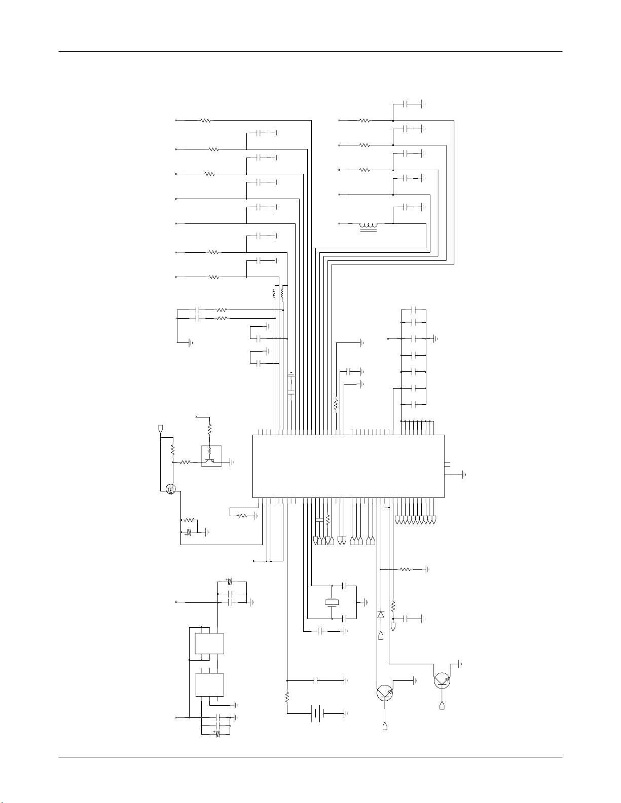
2. SGH-Z510 Flow Chart of Troubleshooting and Circuit Diagrams
2-1.Baseband
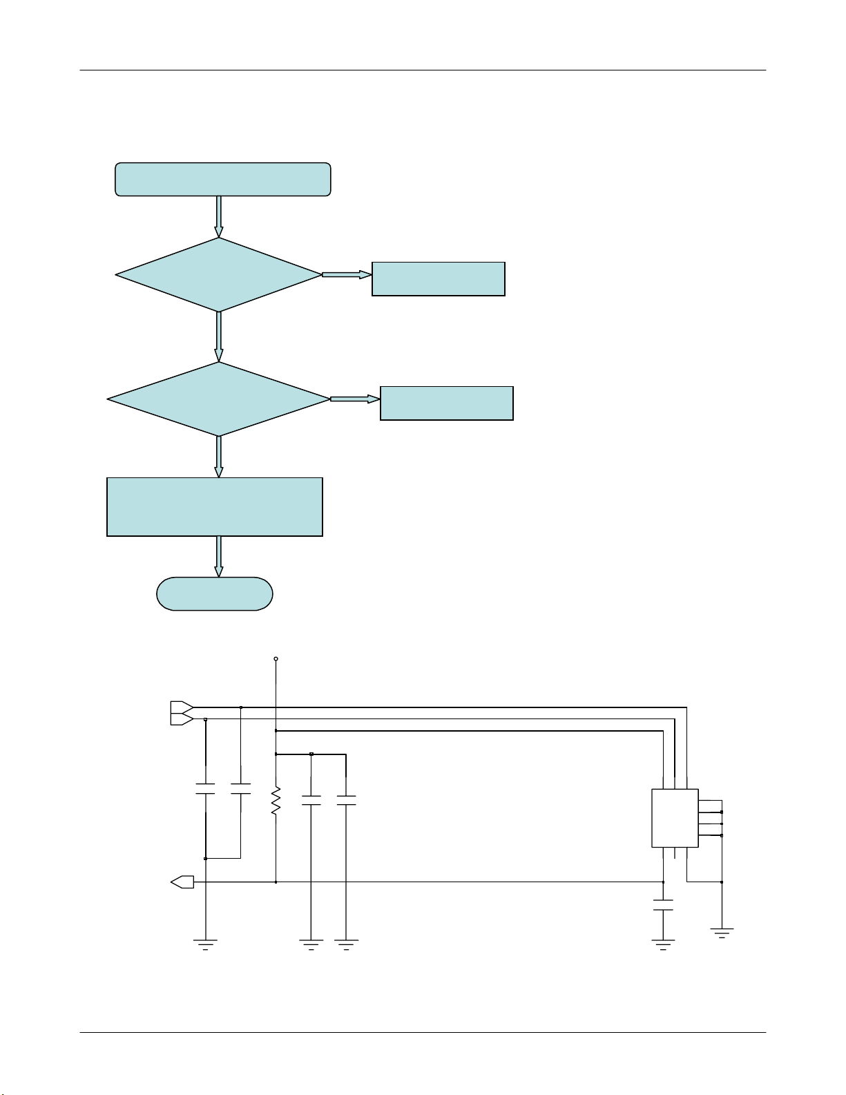
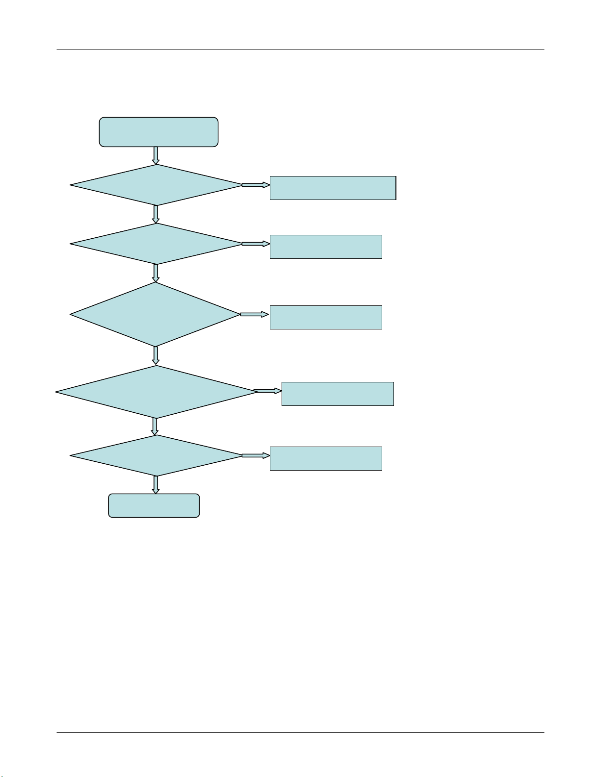
2-1-1. Power ON
Power On does not work
YES
Current Consumption
100mA ?
YES
Check the Battery Voltage
3.3 ?
YES
D501(PS_HOLD)
is High ?
YES
Check U500(PMIC)
Pin #32(VREG_MSMC ) ≒1.25V
Pin #36(VREG_MSME ) ≒1.8V
Pin #50,56(VREG_MSMP,A ) ≒2.6V
Pin #84(VREG_TCXO ) ≒2.85V
pin #3 ,5 (ISNS_M,P) 3.3V
NO
NO
NO
Download Again
Charge the Battery
Check the D501
NO
Check the U500
YES
The pin 53 of U500
19.2MHZ
Vp-p 500mV?
YES
Check the LCD Module
END
SAMSUNG Proprietary-Contents may change without notice
This Document can not be used without Samsung's authorization
NO
Check the TCX300
2-1
SGH-Z510 Flow Chart of Troubleshooting and Circuit Diagrams
3
0
5
T
B
_
V
A
6
.
2
_
V
P
6
.
2
_
V
M
I
S
U
5
8
.
2
_
V
C
I
M
_
V
E
8
.
1
_
V
C
5
2
.
1
_
V
C
C
V
_
B
S
U
0
0
5
1
R
T
2
S
N
I
_
V
T
A
B
V
R
9
0
5
1
R
0
5
5
0
5
R
9
0
5
R
8
0
5
R
7
1
0
0
5
5
R
C
6
0
0
0
5
5
R
C
E
8
.
1
_
V
4
0
5
R
1
1
0
5
R
2
0
5
R
G
3
D
0
0
5
R
0
0
5
A
T
1
0
5
U
0
0
5
U
2
3
1
0
5
R
T
V
0
5
V
0
1
5
4
6
D
S
D
G
D
D
3
2
1
5
4
6
C
E
C
N
T
N
A
G
G
D
A
N
L
N
I
G
F
2
3
1
3
0
5
C
0
V
1
1
0
2
V
0
5
C
1
0
5
A
T
C
8
0
5
C
3
1
5
C
2
1
5
C
1
1
5
C
0
1
5
C
1
0
0
0
5
5
L
L
6
0
5
C
7
0
5
C
5
1
5
C
7
1
8
4
2
7
2
1
1
2
V
A
A
V
5
5
P
P
_
_
_
_
G
G
W
W
E
E
S
S
R
V
R
V
V
V
2
0
5
U
S
U
B
P
M
V
_
_
G
_
S
S
H
B
N
N
S
C
S
S
V
I
I
U
2
6
3
5
1
1
1
5
R
N
I
_
V
2
0
5
A
T
5
0
C
5
4
0
5
C
0
0
6
2
2
9
3
3
5
1
3
4
3
3
B
E
P
E
C
C
C
M
I
S
M
M
M
M
M
M
U
U
S
S
S
S
S
M
R
_
_
M
M
M
M
M
_
G
_
_
_
_
_
G
G
E
G
G
E
G
W
W
E
R
E
E
E
R
S
S
R
V
R
R
R
V
V
V
V
V
V
V
N
N
N
_
_
_
P
L
P
L
T
T
U
Y
T
E
C
K
B
C
F
N
_
I
_
_
T
C
_
G
O
C
B
A
T
A
H
S
C
B
A
D
B
C
V
V
B
A
V
U
6
4
0
7
1
8
5
6
4
1
2
1
5
R
S
P
O
O
X
C
T
5
8
.
2
_
V
C
S
O
5
8
.
2
_
V
X
T
5
8
.
2
_
V
X
R
5
8
.
2
_
V
1
X
R
5
8
.
2
_
V
4
1
5
R
4
1
3
6
7
9
1
3
4
8
8
7
5
6
6
6
6
6
2
1
T
T
P
X
A
N
O
X
X
E
T
N
Y
A
X
M
F
S
L
R
R
Y
S
M
_
G
E
R
V
N
I
_
L
A
T
X
4
4
B
C
I
_
F
F
R
S
_
T
W
F
_
_
R
R
_
F
_
E
_
_
G
G
E
G
G
R
E
G
G
E
R
E
E
E
E
R
R
R
R
V
R
R
V
V
V
V
V
K
T
T
T
L
2
1
U
U
N
U
C
N
N
N
O
I
I
O
I
E
_
O
_
_
_
_
_
_
P
_
X
X
X
O
O
O
L
E
U
U
U
X
X
X
A
E
M
T
M
M
L
C
C
C
T
T
A
T
X
A
A
S
8
6
2
5
2
0
5
3
5
4
8
5
7
7
4
5
7
1
5
3
C
1
5
R
F
T
T
N
O
N
I
V
U
U
E
X
_
_
O
O
C
L
_
_
O
T
A
X
X
T
O
U
X
C
X
_
T
C
M
P
T
A
E
E
L
S
0
0
5
C
S
O
8
1
5
C
6
1
5
C
1
0
5
T
A
B
G
E
N
1
7
5
1
6
5
1
5
5
5
0
L
2
1
2
5
C
6
5
3
2
2
1
8
7
2
2
2
6
2
P
N
N
N
N
N
D
_
_
_
_
_
_
N
V
V
V
N
V
V
I
G
R
R
R
R
R
_
_
D
D
D
D
D
R
F
_
_
_
_
_
K
E
1
B
H
D
D
P
I
R
P
S
P
C
S
V
L
L
G
K
F
N
T
_
T
0
P
M
E
U
_
_
A
E
D
D
S
D
D
I
O
O
_
_
_
_
_
_
_
F
B
B
B
B
B
B
S
E
S
S
S
S
S
U
R
U
U
U
U
U
0
8
0
9
7
1
3
8
1
2
1
1
1
1
-
+
F
N
O
O
D
D
_
E
P
M
E
R
V
V
_
_
O
_
3
_
B
B
C
B
S
I
S
S
U
U
M
U
P
0
2
5
C
9
1
5
C
2
0
5
R
T
6
2
5
C
R
5
2
5
C
R
4
2
5
C
R
3
2
5
C
2
2
5
C
4
3
5
C
3
3
5
C
N
I
_
1
V
3
5
C
0
3
5
C
9
2
5
C
8
2
5
C
7
2
5
C
5
9
4
8
7
7
7
7
P
P
M
M
_
Y
_
_
T
B
T
N
I
_
U
U
_
R
O
O
R
_
K
_
K
P
R
R
P
S
K
K
S
P
P
S
S
N
N
N
_
_
_
R
R
D
R
L
W
W
W
O
P
P
P
1
0
H
L
L
D
_
B
B
P
S
C
C
K
P
6
8
4
7
6
6
2
5
1
0
5
D
D
L
O
H
_
S
P
3
1
W
S
_
N
O
4
1
7
9
2
5
3
5
4
7
2
5
3
3
A
A
E
R
C
M
M
I
P
N
K
S
M
M
U
_
A
P
S
S
M
R
_
D
S
_
M
M
_
_
D
D
_
D
_
D
V
D
D
D
D
D
D
V
D
V
D
D
V
V
V
V
N
_
T
K
T
L
S
O
E
T
C
I
R
K
S
_
_
_
L
S
E
O
I
C
R
M
M
M
R
_
_
_
_
_
_
_
T
M
M
M
M
M
M
I
I
I
I
I
I
N
D
U
U
U
U
U
U
B
O
R
R
R
R
R
S
R
P
6
8
3
4
0
7
0
9
2
3
4
4
3
4
3
T
T
K
A
A
K
L
L
T
E
T
E
C
A
S
A
S
C
_
_
E
E
D
D
_
_
M
R
M
R
I
_
_
_
M
M
S
I
_
M
M
M
U
S
I
I
_
M
S
S
U
I
M
U
S
U
I
S
U
U
9
1
5
R
8
1
5
R
2
3
5
C
N
I
_
T
E
S
E
R
2
2-2
SAMSUNG Proprietary-Contents may change without notice
This Document can not be used without Samsung's authorization
3
5
1
8
6
7
F
N
N
I
R
A
A
_
L
M
D
W
_
D
_
D
V
D
D
D
V
V
C
N
8
7
C
N
8
6
D
N
G
8
5
N
_
T
N
I
_
K
T
M
S
C
S
B
B
M
S
S
9
1
9
5
5
4
T
T
K
N
S
_
D
C
T
B
B
B
S
N
S
S
I
_
_
_
_
M
M
M
M
P
P
P
P
3
2
3
0
5
R
T
1
N
O
_
G
I
J
SGH-Z510 Flow Chart of Troubleshooting and Circuit Diagrams
2-3
SAMSUNG Proprietary-Contents may change without notice
This Document can not be used without Samsung's authorization
SGH-Z510 Flow Chart of Troubleshooting and Circuit Diagrams
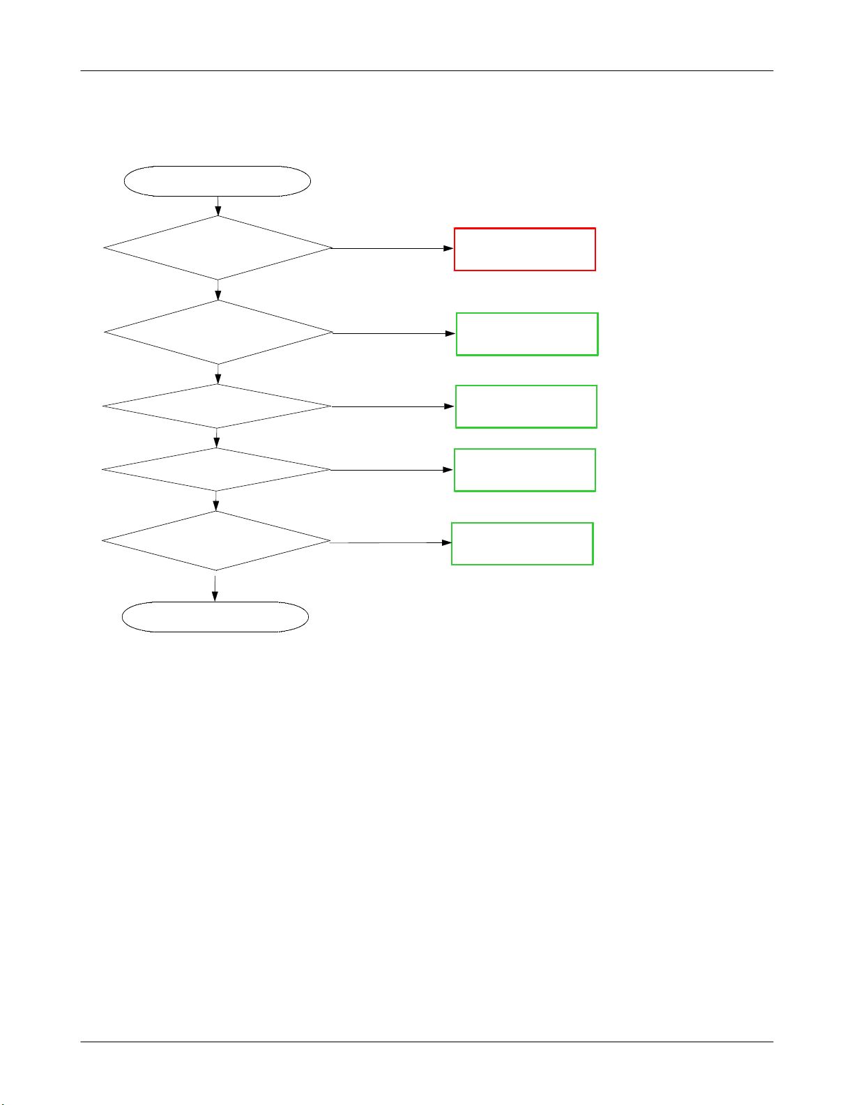
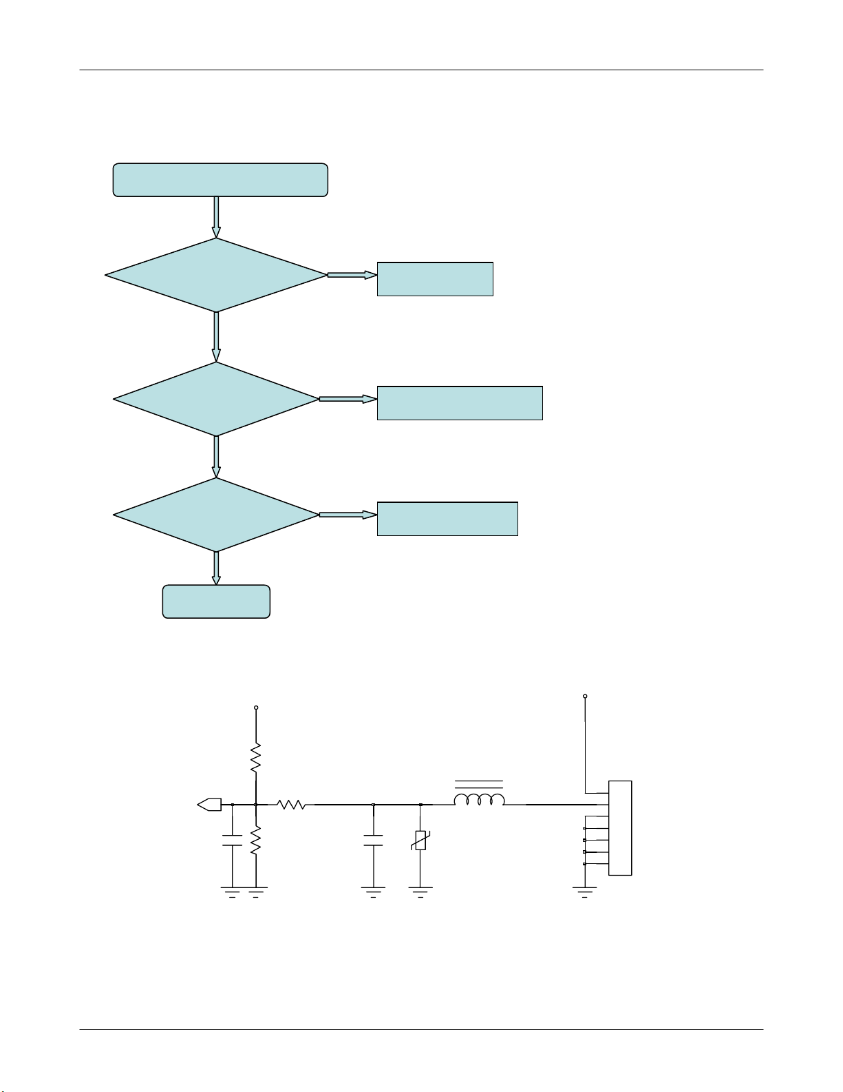
2-1-2. Initial
Initial Failure
Check the
pin 9 of
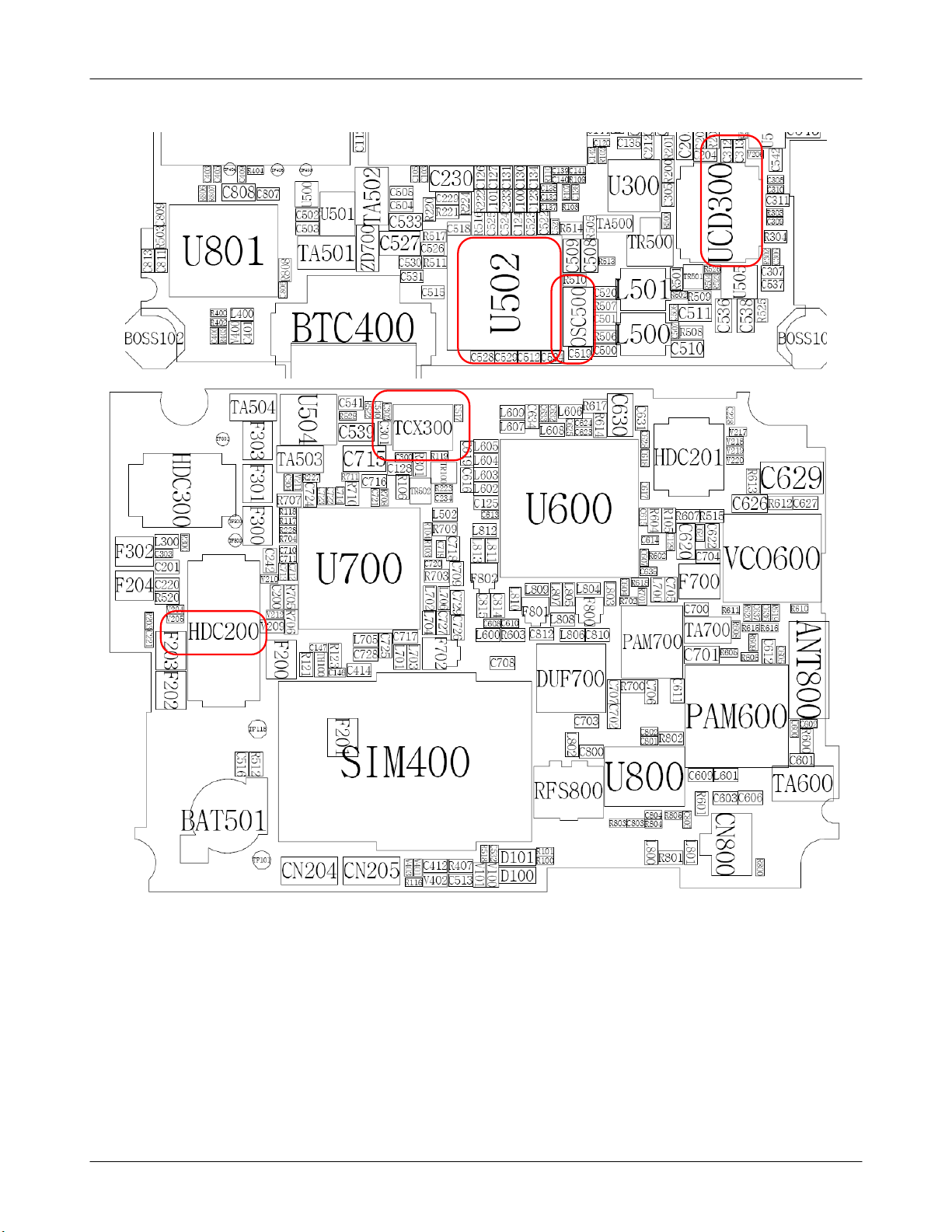
U502 is "High"
YES
Check the Sleep X-
tal signal's at C519
YES
Check the clock
signal's at R513
YES
LCD Display OK ?
YES
Sound operation OK
END
NO
NO
NO
NO
NO
Check U502
Check the OSC500
Check the
Check the HDC200 part
Check the UCD300 part
U502 and
TCX300
2-4
SAMSUNG Proprietary-Contents may change without notice
This Document can not be used without Samsung's authorization
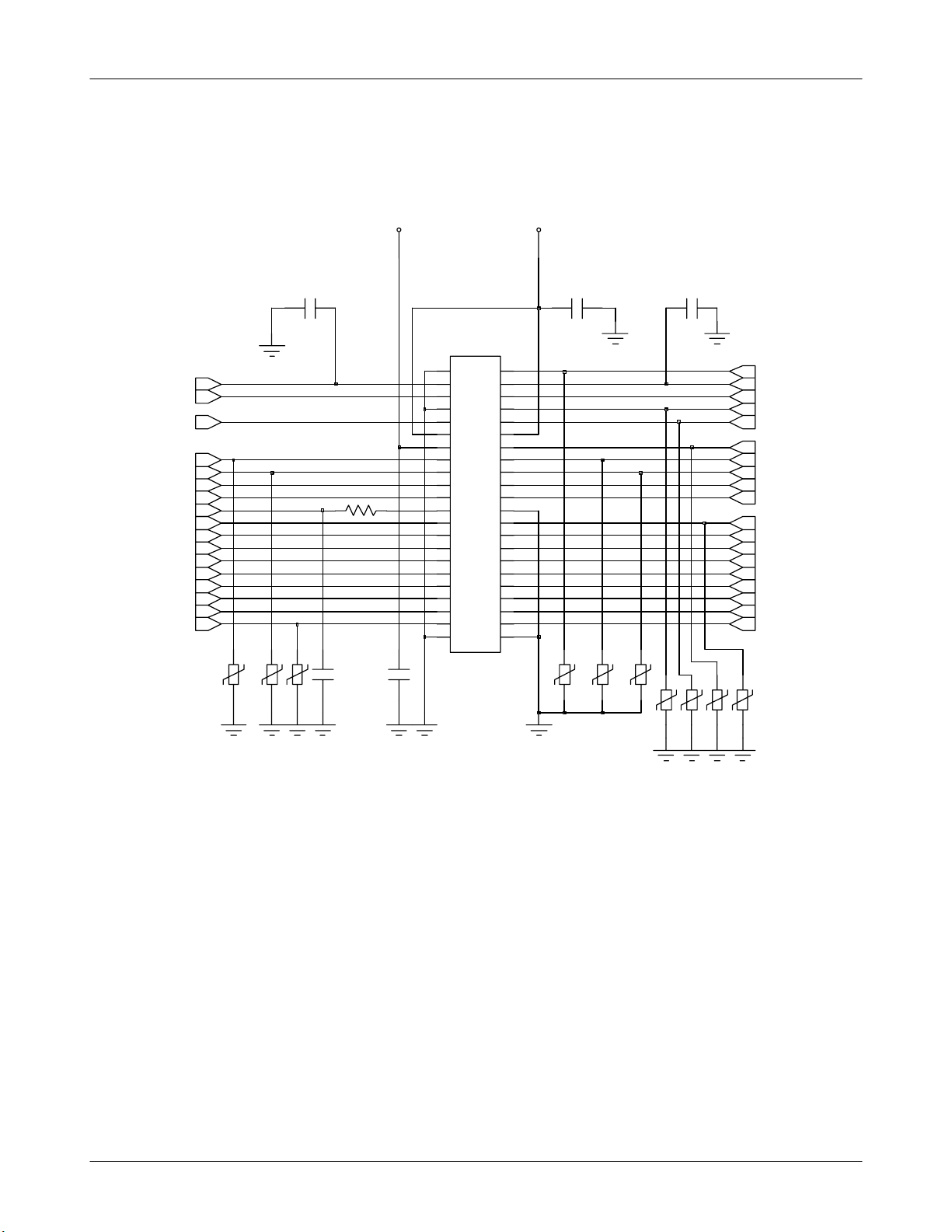
SGH-Z510 Flow Chart of Troubleshooting and Circuit Diagrams
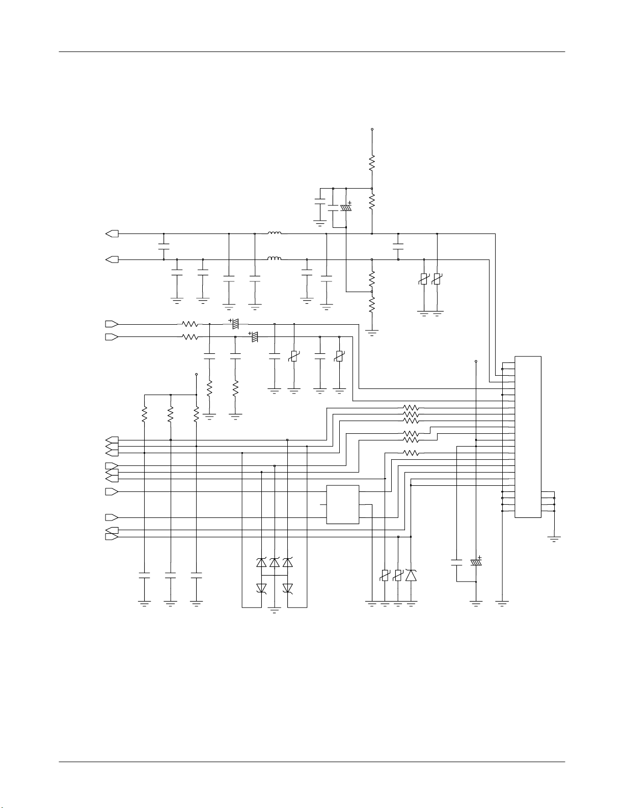
V_2.8LCD V_IN
C201
HDC200
11
ICE_AMP_L
VOICE_OUT_P
VIBRATOR
FLASH_EN1
SCAN_4
ELCD_RS1 ESLCD_CS
ENAND_WE
LCD_RESET
ENAND_D(15)
ENAND_D(13)
ENAND_D(11) ENAND_D(12)
ENAND_D(9) ENAND_D(10)
ENAND_D(7) ENAND_D(8)
ENAND_D(5) ENAND_D(6)
ENAND_D(3) ENAND_D(4)
ENAND_D(1) ENAND_D(2)
SCAN_3
4
0
2
V
6
5
0
0
2
2
V
V
1
2
2
C
(0603)
(0603)
R203
55
99
13 13 14
17 17 18
19
21
23 24
25
27 28
29
31 32
33
35 36
37
39
41 42
43
0
2
2
C
77
1111
1515
19
21 22
23
25 26
27
293330
31
33
35
37 38
39
41
43 44
2
2
44
6
6
8
8
10
10
12
12
14
16
16
18
20
20
22
24
26
28
30
32
34
34
36
38
40
40
42
44
C200
7
8
0
2
V
9
0
0
2
2
V
V
C242
ALERT_LED_R
ICE_AMP_R
VOICE_OUT_N
AMP_EN
KEY_4
AMP_EN2
BACK_LIGHT_EN
HALL_SW
EMLCD_CS
SCAN_5
ENAND_D(14)
ENAND_D(0)
0
1
1
1
2
2
V
V
2
1
2
V
(0603)
3
1
2
V
2-5
SAMSUNG Proprietary-Contents may change without notice
This Document can not be used without Samsung's authorization
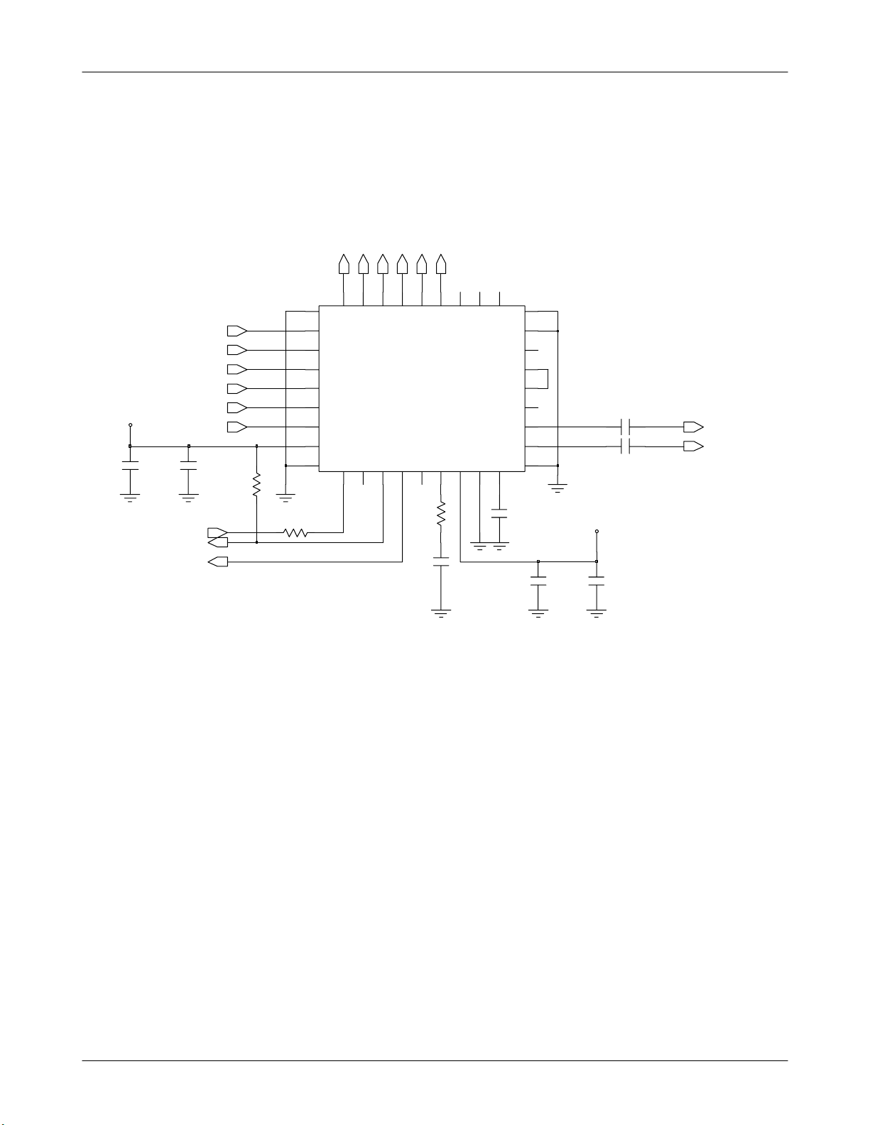
SGH-Z510 Flow Chart of Troubleshooting and Circuit Diagrams
V_2.6P
NAND_D(1)
NAND_D(0)
NAND_WE
YMU_CS_N
YMU_A0
NAND_RE
C307
TCXO_OUT
YMU_IRQ
YMU_RST_N
C306
R302
R304
33
26
27
28
29
30
31
32
34
25
G
D1
D0
/WR
/CS
A0
/RD
IOVDD
G
1
)
)
)
3
2
4
(
(
(
D
D
D
_
_
_
D
D
D
N
N
N
A
A
A
N
N
N
22
24
4
2
3
D
D
D
UCD300
I
K
Q
D
L
E
R
I
/
L
C
3
4
2
)
5
(
D
_
D
N
A
N
21
5
D
T
S
R
/
C309
5
R303
)
6
(
D
_
D
N
A
N
20
6
D
C
N
6
)
7
(
D
_
D
N
A
N
17
1923
18
7
D
1
2
R
T
T
T
U
U
M
SPVSS
O
O
P
P
S
S
SPVDD
EQ3
EQ2
EQ1
HPOUT-R
HPOUT-L/MONO
C
L
L
P
7
F
D
E
S
D
R
S
V
V
V
8
9
G
G
C308
36
16
15
14
13
12
11
10
C312
C313
YMU_OUT_R
YMU_OUT_L
35
V_YMU
C310
C311
2-6
SAMSUNG Proprietary-Contents may change without notice
This Document can not be used without Samsung's authorization
SGH-Z510 Flow Chart of Troubleshooting and Circuit Diagrams
2-7
SAMSUNG Proprietary-Contents may change without notice
This Document can not be used without Samsung's authorization
SGH-Z510 Flow Chart of Troubleshooting and Circuit Diagrams
2-1-3. Sim Part
Power Can not access SIM Card
YES
Check the Voltage at pin 1 of
SIM400 ≒2.85V
YES
Check the SIM400’s Connection
To SIM card
YES
Check the circuit around UME400 and
Data stored in it
END
V_2.85USIM
NO
Check the circuit
Related to SIM400
NO
Resolder SIM400
USIM_CLK
USIM_RESET
USIM_DATA
C410
C411
C412
R407
C413
2-8
SAMSUNG Proprietary-Contents may change without notice
This Document can not be used without Samsung's authorization
C414
2
1
3
SIM400
2
1
3
G
0
1
9
G
G
8
G
5
6
4
6
7
4
5

SGH-Z510 Flow Chart of Troubleshooting and Circuit Diagrams
2-9
SAMSUNG Proprietary-Contents may change without notice
This Document can not be used without Samsung's authorization
SGH-Z510 Flow Chart of Troubleshooting and Circuit Diagrams
2-1-4. Charging Part
Abnormal Charging Operation
YES
Check the Pin #13,#14 of IFC200
(Vbat) 3.3
YES
Check the Pin #1 of BTC400
(Vbat) 3.3
YES
See the indicator of charger is
red ?
YES
END
NO
NO
NO
Check the TA
Check the Path of IFC200
and BTC400
Check around of U502
(PM6650)
VF
V_2.85TCXO
R400
L400
C400
R403
R402
C401
0
0
4
V
2-10
SAMSUNG Proprietary-Contents may change without notice
This Document can not be used without Samsung's authorization
VBAT
BTC400
1
1
2
2
3
3
4
NC
5
NC
6
NC
7
NC
SGH-Z510 Flow Chart of Troubleshooting and Circuit Diagrams
V_MIC
R200
0
MIC2P
MIC2N
EAR_R
EAR_L
EAR_SW
JACK_IN
ADC_BOOTSW
TXD_1
RXD_1
JIG_ON_IF
USB_VCC
TA_VEXT
D+
D-
R211 R212
C209
C206
R205
R206
V_2.6P
R210
C210
C212
C214
C215
C213
R208R207
C204
L200
L201
C208
V202
C217C216
C218
456
C219
6
5
4
C211
D
VBUS
D
C203
V203
GND
U200
C205
D
D
R201
C207
33PF
V200
C223
C222
VBAT
IFC200
1
1
2
2
3
3
4
4
5
5
6
6
7
7
8
8
9
9
10
10
11
11
12
12
13
13
14
14
15
15
16
16
17
17
18
18
19
19
20
20
21
22
23
24
25
NC
NC
26
NC
NC
27
NC
NC
28
NC
NC
R209
R213
R214
R215
R216
R217
V201
R202
R204
(0603)
(0603)
(0603)
(0603)
(0603)
1
2
3
C226
C225
C224
5
1
2
1
3
2
ZD201
V
2-11
SAMSUNG Proprietary-Contents may change without notice
This Document can not be used without Samsung's authorization
4
ZD200
1
2
V

SGH-Z510 Flow Chart of Troubleshooting and Circuit Diagrams
2-12
SAMSUNG Proprietary-Contents may change without notice
This Document can not be used without Samsung's authorization
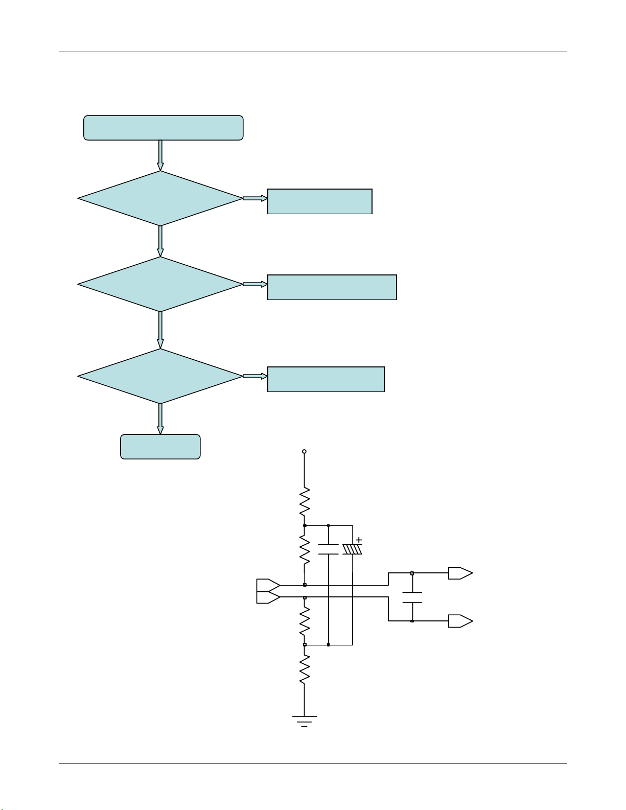
2-1-5. Microphone Part
Micro-Phone does not work
YES
SGH-Z510 Flow Chart of Troubleshooting and Circuit Diagrams
Is the assembled status of
Microphone O.K?
YES
Check the Voltage of R220
Is ≒ 2.9V
YES
IS Microphone OK?
YES
END
NO
Reassemble Microphone
NO
Check the Path around MIC
NO
Check UCP100(MSM6250)
Bias circuit
V_MIC
R220
C229
C230
R221
MIC1P
MIC1N
C233
R222
R224
2-13
SAMSUNG Proprietary-Contents may change without notice
This Document can not be used without Samsung's authorization
MIC1P
MIC1N

SGH-Z510 Flow Chart of Troubleshooting and Circuit Diagrams
2-14
SAMSUNG Proprietary-Contents may change without notice
This Document can not be used without Samsung's authorization
2-1-6. Speaker
Speaker does not work
YES
SGH-Z510 Flow Chart of Troubleshooting and Circuit Diagrams
Check the UCD300(Yamaha)
Pin#1 ≒ 19.2MHz
YES
Check the UCD300
Pin#32 ≒ 2.6V
YES
Are there any signal
at the Pin#10, 22 of U4
(SAPA1D2, LCD Module)?
YES
Are there any signal at the
Pin# 3,4,11,12 of J5 ( in LCD Module)?
YES
Is Speaker working?
NO
NO
NO
NO
Check the U502, R 513
≒ 19.2 MHz
Check the U502(PM6650)
Check the
U300(STG3699A)
NO
Check the U4(SAPA1D2)
Replace the Speaker
END
2-15
SAMSUNG Proprietary-Contents may change without notice
This Document can not be used without Samsung's authorization

SGH-Z510 Flow Chart of Troubleshooting and Circuit Diagrams
2-1-7. Receiver Part
Receiver does not work
YES
Terminal of receiver is ok?
YES
Are there any signal
at the 5, 6 pin of HDC200
Check the LCD Module
END
NO
Replace the Speaker ass’y
NO
Check the U100(MSM6250)
2-16
SAMSUNG Proprietary-Contents may change without notice
This Document can not be used without Samsung's authorization
SGH-Z510 Flow Chart of Troubleshooting and Circuit Diagrams
R
R
_
_
T
P
U
M
O
A
_
_
U
E
M
C
I
Y
MSM_EAR_R
AUD_SEL_1
YMU_OUT_L
ICE_AMP_L
21
22
1
2
3
4
17
NC
NC
1S2
1-2IN
2S1
D2
15
D
1
N
D
G
U300
2
S
2
6
5
1316
14
1
+
S
V
1
D
1
N
S
3
G
7
8
L
_
R
A
E
_
M
S
M
2
S
4
D4
4S1
3-4IN
3S2
3
D
12
11
10
V_2.6A
C305
EAR_L
YMU_OUT_L
AUD_SEL_2
9
MSM_EAR_R
L
_
R
A
E
_
M
S
M
2-17
SAMSUNG Proprietary-Contents may change without notice
This Document can not be used without Samsung's authorization
R
_
T
U
O
_
U
M
Y
R
_
R
A
E
 Loading...