

Samsung Z100 Service Manual COVER
UMTS TELEPHONE
SGH-Z100
Manual
SERVICE
UMTS TELEPHONE CONTENTS
1. Specification
2. Circuit Description
3. Exploded Views and Parts List
4. Electrical Parts List
5. Block Diagrams
6. PCB Diagrams
7. Flow Chart of Troubleshooting
ELECTRONICS
This Service Manual is a property of Samsung Electronics Co.,Ltd.
Any unauthorized use of Manual can be punished under applicable
International and/or domestic law.
Samsung Electronics Co.,Ltd. June. 2003
ⓒ
Printed in Korea.
Code No.: GH68-04553A
BASIC.
1. SGH-Z100 Specification
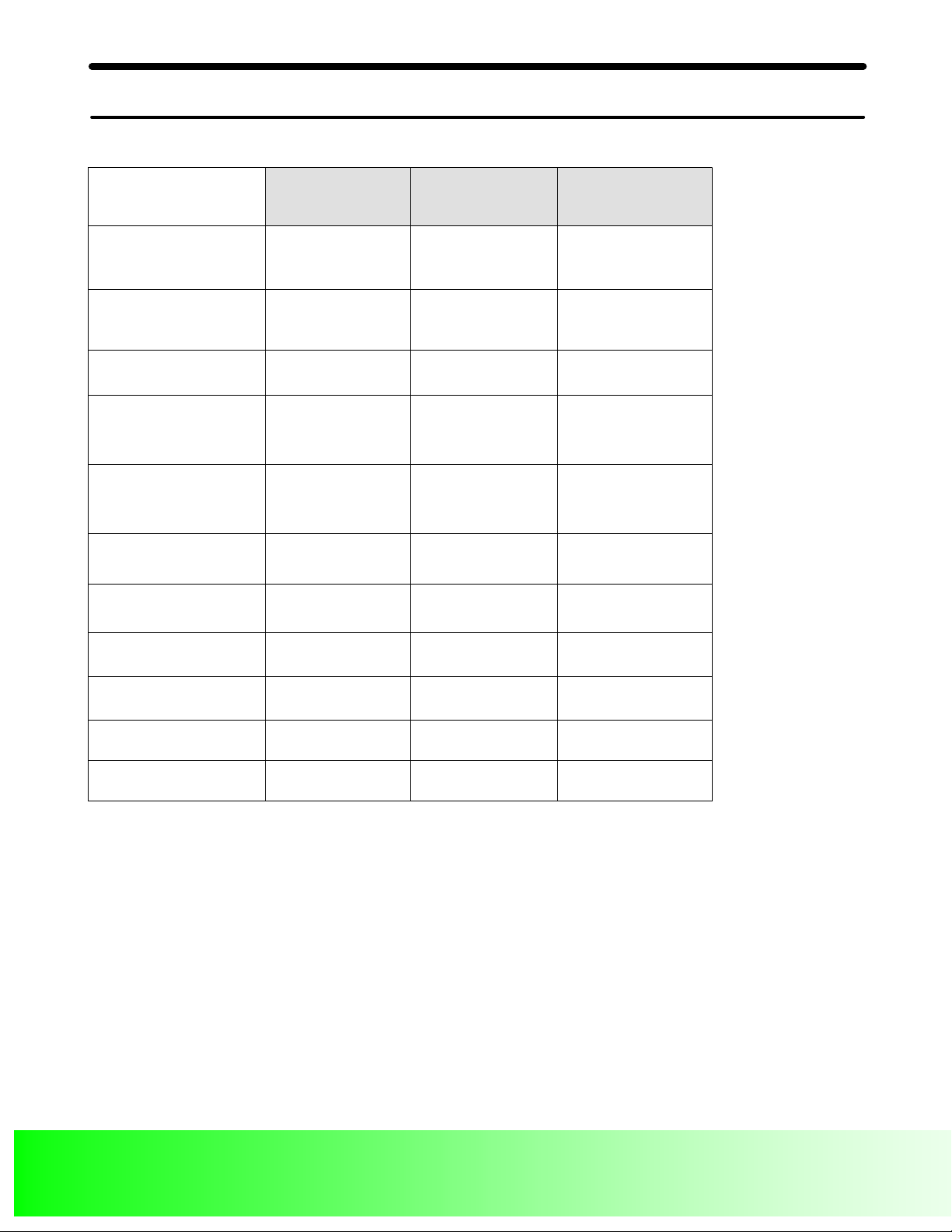
1. GSM General Specification
GSM900
Pha s e 1
Freq. Band[MHz]
Uplink/ D ownlink
ARFCN range 1~124
T x/Rx spacing 45MHz 45MHz 95MHz
Mod. Bit rate/
Bit Period
T ime Slot
Period/Frame Period
Modulation 0.3GMSK 0.3GMSK 0.3GMSK
MS Power 33dBm~13dBm 33dBm~5dBm 30dBm~0dBm
890~915
935~960
270.833kbps
3.692us
576.9us
4.615ms
EGSM 900
Pha s e 2
880~915
925~960
0~124 &
975~1023
270.833kbps
3.692us
576.9us
4.615ms
DCS1800
1710~1785
1805~1880
270. 833kbps
Phase 1
512~885
3.692us
576. 9us
4.615ms
Power Class 5pcl ~ 15pcl 5pcl ~ 19pcl 0pcl ~ 15pcl
Sensitivit y -102dBm -102dBm -100dBm
TDMA Mux 8 8 8
Cell Radius 35Km 35Km 2Km
1-1
SAMSUNG Proprietary-Contents may change without notice
This Document ca not be u ed without Samsung's authorization
Email: ICQ: 343183001 QQ: 35070846
SGH-Z100 Specification
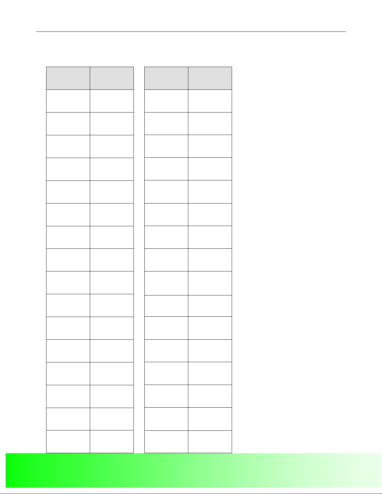
2. GSM TX power class
TX Power
control level
5 33±2 dBm
6 31±2 dBm
7 29±2 dBm
8 27±2 dBm
9 25±2 dBm
10 23±2 dBm
11 21±2 dBm
GSM900
TX Power
control level
0 30±3 dBm
1 28±3 dBm
2 26±3 dBm
3 24±3 dBm
4 22±3 dBm
5 20±3 dBm
6 18±3 dBm
DCS1800
12 19±2 dBm
13 17±2 dBm
14 15±2 dBm
15 13±2 dBm
16 11±3 dBm
17 9±3dBm
18 7±3 dBm
19 5±3 dBm
7 16±3 dBm
8 14±3 dBm
9 12±4 dBm
10 10±4 dBm
11 8±4dBm
12 6±4 dBm
13 4±4 dBm
14 2±5 dBm
15 0±5 dBm
1-2
SAMSUNG Proprietary-Contents may change without notice
1. SGH-Z100 Specification
3. WCDMA General Specification
W CDMA (FDD)
Freq. Band[MHz]
Uplink/ D ownlink
ARFCN range
Uplink/ D ownlink
T x/Rx spacing 190MHz
Mod. Bit rate 3.84Mcps
T ime Slot
Period/Frame Period
Modulation QPSK/HPSK
MS Power
(Cla s s3)
Power Class 3
1920~1980
2110~2170
9612~9888
10562~10838
24dBm~-50dBm
667us
10ms
Sensitivit y -106.7dBm
Modulat in filter RRC(α= 0.22)
Voi ce code c AMR
2. WCDMA TX power class
TX Power
class
1 33(+1/-3) dBm
2 27(+1/-3) dBm
3 24(+1/-3) dBm
4 21(+1/-3) dBm
WCDMA
1-3
SAMSUNG Proprietary-Contents may change without notice
Email: ICQ: 343183001 QQ: 35070846

2. SGH-Z100 Circuit Description
1. SGH-Z100 RF Circuit Description
1. Antenna Switch Module (U100)
The antenna switch module allows multiple operating bands and modes to share the same antenna. A common antenna
connects to one of five paths: 1) UMTS-2100 Rx/Tx, 2) EGSM-900 Rx, 3) EGSM-900 Tx, 4) DCS-1800 Rx, and 5)
DCS-1800 Tx. UMTS operation requires simultaneous reception and transmission.
2. Filter
To convert Electromagnetic Field Wave to Acoustic Wave and then pass the specific frequency band.
- GSM Rx FILTER (F100)→For filtering the frequency band between 925 ~ 960 MHz
- DCS Rx FILTER (F101)→For filtering the frequency band 1805 and 1880 MHz.
- WCDMA Rx FILTER (F203)→For filtering the frequency band 2110 and 2170 MHz.
- WCDMA Tx FILTER (F200)→For filtering the frequency band 1920 and 1980 MHz.
3. TCVCXO (OSC200)
To generate the 19.2MHz reference clock to drive the logic and RF.
4. Duplexer (F202)
A duplexer splits a single operating band into receive and transmit paths.
5. Isolator (MIS1)
An isolator between the Power Amplifier and the duplexer is highly recommended to provide constant load and source
impedances (respectively) to those devices.
6. UMTS PAM (U200)
This is a key component in the transmitter chain and must complement the RTR6200 IC precisely; jointly they dominate
the UMTS transmitter performance characteristics. Parameters such as gain, output power level, ACLR, harmonics, Rx-band
noise, and power supply current are critical.
7. GSM/DCS PAM (U102)
The PAM is a key component in any transmitter chain and must complement the rest of the transmitter precisely. For
GSM and DCS operation, the closed-loop transmit power control functions add even more requirements relative to the
UMTS PA. In addition to gain control and switching requirements, the usual RF parameters such as gain, output power
level, several output spectrum requirements, and power supply current are critical.
8. GSM/DCS Dual Tx VCO (OSC100)
The dual Tx VCO outputs, one for EGSM and one for DCS, drive a resistive network that splits the active signal into
two signals: 1) the input to the active PAM – this is the low loss path, and 2) the OPLL feedback signal.
9. Dual VCO (OSC201)
The dual-band UHF VCO is a key component within its phase-locked loop; VCO performance directly impacts PLL and
transceiver performance. GSM/DCS Rx/Tx LO & UMTS Rx LO signal is generated from this dual VCO's output.
2-1
SAMSUNG Proprietary-Contents may change without notice
Email: ICQ: 343183001 QQ: 35070846
 Loading...