

Samsung WS32Z78RSMXXEG Service Manual
COLOR TELEVISION RECEIVER
Chassis : S57A(P)_Rev.1
Model : WS32Z78RSMXXEG
COLOR TELEVISION RECEIVER CONTENTS
Precautions
Reference Information
Specifications
Alignment and Adjustments
Exploded Views and Parts List
Electrical Parts List
Block Diagrams
Schematic Diagrams
1.
2.
3.
4.
5.
6.
7.
8.
1. Precautions
1-1 Safety Precautions
1. Be sure that all of the built-in protective
devices are replaced. Restore any missing
protective shields.
2. When reinstalling the chassis and its
assemblies, be sure to restore all protective
devices, including: nonmetallic control knobs
and compartment covers.
3. Make sure that there are no cabinet openings
through which people—particularly
children—might insert fingers and contact
dangerous voltages. Such openings include
the spacing between the picture tube and the
cabinet mask, excessively wide cabinet
ventilation slots, and improperly fitted back
covers.
If the measured resistance is less than 1.0
megohm or greater than 5.2 megohms, an
abnormality exists that must be corrected
before the unit is returned to the customer.
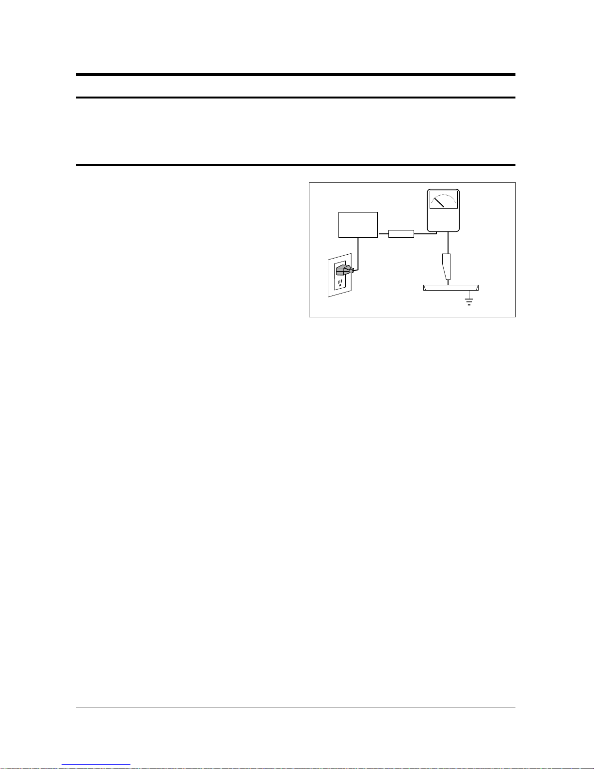
4. Leakage Current Hot Check (Figure 1-1):
Warning: Do not use an isolation
transformer during this test. Use a leakagecurrent tester or a metering system that
complies with American National Standards
Institute (ANIS C101.1, Leakage Current for
Appliances), and Underwriters Laboratories
(UL Publication UL1410, 59.7).
5. With the unit completely reassembled, plug
the AC line cord directly into the power
outlet. With the unit’s AC switch first in the
ON position and then OFF, measure the
current between a known earth ground (metal
water pipe, conduit, etc.) and all exposed
metal parts, including: antennas, handle
brackets, metal cabinets, screwheads and
control shafts. The current measured should
not exceed 0.5 milliamp. Reverse the powerplug prongs in the AC outlet and repeat the
test.
Fig. 1-1 AC Leakage Test
6. Antenna Cold Check:
With the unit’s AC plug disconnected from the
AC source, connect an electrical jumper across
the two AC prongs. Connect one lead of the
ohmmeter to an AC prong. Connect the other
lead to the coaxial connector.
7. X-ray Limits:
The picture tube is especially designed to
prohibit X-ray emissions. To ensure continued
X-ray protection, replace the picture tube only
with one that is the same type as the original.
Carefully reinstall the picture tube shields and
mounting hardware; these also provide X-ray
protection.
8. High Voltage Limits:
High voltage must be measured each time
servicing is done on the B+, horizontal
deflection or high voltage circuits.
Correct operation of the X-ray protection
circuits must be reconfirmed whenever they
are serviced.
(X-ray protection circuits also may be called
“horizontal disable” or “hold-down”.)
Heed the high voltage limits. These include
the X–ray Protection Specifications Label, and
the Product Safety and X-ray Warning Note on
the service data schematic.
Precautions
Samsung Electronics 1-1
LEAKAGE
CURRENT
TESTER
DEVICE
UNDER
TEST
TEST ALL
EXPOSED METAL
SURFACES
3-WIRE CORD
ALSO TEST WITH
PLUG REVERSED
(USING AC ADAPTER
PLUG AS REQUIRED)
EARTH
GROUND
(READING SHOULD
NOT BE ABOVE
0.5mA)
Follow these safety, servicing and ESD precautions to prevent damage and protect against potential
hazards such as electrical shock and X-rays.

1-1 Safety Precautions (Continued)
9. High voltage is maintained within specified
limits by close-tolerance, safety-related
components and adjustments. If the high
voltage exceeds the specified limits, check
each of the special components.
10. Design Alteration Warning:
Never alter or add to the mechanical or
electrical design of this unit. Example: Do not
add auxiliary audio or video connectors. Such
alterations might create a safety hazard. Also,
any design changes or additions will void the
manufacturer’s warranty.
11. Hot Chassis Warning:
Some TV receiver chassis are electrically
connected directly to one conductor of the AC
power cord. If an isolation transformer is not
used, these units may be safely serviced only
if the AC power plug is inserted so that the
chassis is connected to the ground side of the
AC source.
To confirm that the AC power plug is inserted
correctly, do the following: Using an AC
voltmeter, measure the voltage between the
chassis and a known earth ground. If the
reading is greater than 1.0V, remove the AC
power plug, reverse its polarity and reinsert.
Re-measure the voltage between the chassis
and ground.
12. Some TV chassis are designed to operate with
85 volts AC between chassis and ground,
regardless of the AC plug polarity. These units
can be safely serviced only if an isolation
transformer inserted between the receiver and
the power source.
13. Some TV chassis have a secondary ground
system in addition to the main chassis ground.
This secondary ground system is not
isolated from the AC power line. The two
ground systems are electrically separated by
insulating material that must not be defeated
or altered.
14. Components, parts and wiring that appear to
have overheated or that are otherwise
damaged should be replaced with parts that
meet the original specifications. Always
determine the cause of damage or
overheating, and correct any potential
hazards.
15. Observe the original lead dress, especially
near the following areas: Antenna wiring,
sharp edges, and especially the AC and high
voltage power supplies. Always inspect for
pinched, out-of-place, or frayed wiring. Do
not change the spacing between components
and the printed circuit board. Check the AC
power cord for damage. Make sure that leads
and components do not touch thermally hot
parts.
16. Picture Tube Implosion Warning:
The picture tube in this receiver employs
“integral implosion” protection. To ensure
continued implosion protection, make sure
that the replacement picture tube is the same
as the original.
17. Do not remove, install or handle the picture
tube without first putting on shatterproof
goggles equipped with side shields. Never
handle the picture tube by its neck. Some
“in-line” picture tubes are equipped with a
permanently attached deflection yoke; do not
try to remove such “permanently attached”
yokes from the picture tube.
18. Product Safety Notice:
Some electrical and mechanical parts have
special safety-related characteristics which
might not be obvious from visual inspection.
These safety features and the protection they
give might be lost if the replacement
component differs from the original—even if
the replacement is rated for higher voltage,
wattage, etc.
Components that are critical for safety are
indicated in the circuit diagram by shading,
( ) or ( ).
Use replacement components that have the
same ratings, especially for flame resistance
and dielectric strength specifications.
A replacement part that does not have the
same safety characteristics as the original
might create shock, fire or other hazards.
Precautions
1-2 Samsung Electronics
!

1-2 Servicing Precautions
1. Servicing precautions are printed on the
cabinet. Follow them.
2. Always unplug the unit’s AC power cord from
the AC power source before attempting to:
(a) Remove or reinstall any component or
assembly, (b) Disconnect an electrical plug or
connector, (c) Connect a test component in
parallel with an electrolytic capacitor.
3. Some components are raised above the printed
circuit board for safety. An insulation tube or
tape is sometimes used. The internal wiring is
sometimes clamped to prevent contact with
thermally hot components. Reinstall all such
elements to their original position.
4. After servicing, always check that the screws,
components and wiring have been correctly
reinstalled. Make sure that the portion around
the serviced part has not been damaged.
5. Check the insulation between the blades of the
AC plug and accessible conductive parts
(examples: metal panels, input terminals and
earphone jacks).
6. Insulation Checking Procedure: Disconnect the
power cord from the AC source and turn the
power switch ON. Connect an insulation
resistance meter (500V) to the blades of the AC
plug.
The insulation resistance between each blade
of the AC plug and accessible conductive parts
(see above) should be greater than 1 megohm.
7. Never defeat any of the B+ voltage interlocks.
Do not apply AC power to the unit (or any of
its assemblies) unless all solid-state heat sinks
are correctly installed.
8. Always connect a test instrument’s ground
lead to the instrument chassis ground before
connecting the positive lead; always remove
the instrument’s ground lead last.
9. If the TV set malfunctions under bad weather
like lightning, check if the parts at the following locations are broken not.
Location : FP801S, C813, FD802S, D805, D801,
IC803S
Precautions
Samsung Electronics 1-3
Warning1: First read the “Safety Precautions” section of this manual. If some unforeseen circumstance creates a conflict between
the servicing and safety precautions, always follow the safety precautions.
Warning2: An electrolytic capacitor installed with the wrong polarity might explode.

1. Some semiconductor (“solid state”) devices
are easily damaged by static electricity. Such
components are called Electrostatically
Sensitive Devices (ESDs); examples include
integrated circuits and some field-effect
transistors. The following techniques will
reduce the occurrence of component damage
caused by static electricity.
2. Immediately before handling any semicon
ductor components or assemblies, drain the
electrostatic charge from your body by
touching a known earth ground. Alternatively,
wear a discharging wrist-strap device. (Be
sure to remove it prior to applying power—
this is an electric shock precaution.)
3. After removing an ESD-equipped assembly,
place it on a conductive surface such as
aluminum foil to prevent accumulation of
electrostatic charge.
4. Do not use freon-propelled chemicals. These
can generate electrical charges that damage
ESDs.
5. Use only a grounded-tip soldering iron when
soldering or unsoldering ESDs.
6. Use only an anti-static solder removal device.
Many solder removal devices are not rated as
“anti-static”; these can accumulate sufficient
electrical charge to damage ESDs.
7. Do not remove a replacement ESD from its
protective package until you are ready to
install it. Most replacement ESDs are
packaged with leads that are electrically
shorted together by conductive foam,
aluminum foil or other conductive materials.
8. Immediately before removing the protective
material from the leads of a replacement ESD,
touch the protective material to the chassis or
circuit assembly into which the device will be
installed.
9. Minimize body motions when handling
unpackaged replacement ESDs. Motions such
as brushing clothes together, or lifting a foot
from a carpeted floor can generate enough
static electricity to damage an ESD.
Precautions
1-4 Samsung Electronics
1-3 Precautions for Electrostatically Sensitive Devices (ESDs)

Reference Information
Samsung Electronics 2-1
2. Reference Information
2-1 Tables of Abbreviations and Acronyms
A
Ah
Å
dB
dBm
°C
°F
°K
F
G
GHz
g
H
Hz
h
ips
kWh
kg
kHz
kΩ
km
km/h
kV
kVA
kW
I
MHz
Ampere
Ampere-hour
Angstrom
Decibel
Decibel Referenced to One
Milliwatt
Degree Celsius
Degree Fahrenheit
degree Kelvin
Farad
Gauss
Gigahertz
Gram
Henry
Hertz
Hour
Inches Per Second
Kilowatt-hour
Kilogram
Kilohertz
Kilohm
Kilometer
Kilometer Per Hour
Kilovolt
Kilovolt-ampere
Kilowatt
Liter
Megahertz
MV
MW
MΩ
m
µA
µF
µH
µm
µs
µW
mA
mg
mH
mI
mm
ms
mV
nF
Ω
pF
Ib
rpm
rps
s
V
VA
W
Wh
Megavolt
Megawatt
Megohm
Meter
Microampere
Microfarad
Microhenry
Micrometer
Microsecond
Microwatt
Milliampere
Milligram
Millihenry
Milliliter
Millimeter
Millisecond
Millivolt
Nanofarad
Ohm
Picofarad
Pound
Revolutions Per Minute
Revolutions Per Second
Second (Time)
Volt
Volt-ampere
Watt
Watt-hour
Table 2-1 Abbreviations

Reference Information
2-2 Samsung Electronics
Table 2-2 Table of Acronyms
ABL
AC
ACC
AF
AFC
AFT
AGC
AM
ANSI
APC
APC
A/V
AVC
BAL
BPF
B-Y
CATV
CB
CCD
CCTV
Ch
CRT
CW
DC
DVM
EIA
ESD
ESD
FBP
FBT
FF
FM
FS
GND
G-Y
H
HF
HI-FI
IC
IC
IF
Automatic Brightness Limiter
Alternating Current
Automatic Chroma Control
Audio Frequency
Automatic Frequency Control
Automatic Fine Tuning
Automatic Gain Control
Amplitude Modulation
American National Standards Institute
Automatic Phase Control
Automatic Picture Control
Audio-Video
Automatic Volume Control
Balance
Bandpass Filter
Blue-Y
Community Antenna Television (Cable TV)
Citizens Band
Charge Coupled Device
Closed Circuit Television
Channel
Cathode Ray Tube
Continuous Wave
Direct Current
Digital Volt Meter
Electronics Industries Association
Electrostatic Discharge
Electrostatically Sensitive Device
Feedback Pulse
Flyback Transformer
Flip-Flop
Frequency Modulation
Fail Safe
Ground
Green-Y
High
High-Frequency
High Fidelity
Inductance-Capacitance
Integrated Circuit
Intermediate Frequency
I/O
L
L
LED
LF
MOSFET
MTS
NAB
NEC
NTSC
OSD
PCB
PLL
PWM
QIF
R
RC
RF
R-Y
SAP
SAW
SIF
SMPS
S/N
SW
TP
TTL
TV
UHF
UL
UV
VCD
VCO
VCXO
VHF
VIF
VR
VTR
VTVM
TR
Input/output
Left
Low
Light Emitting Diode
Low Frequency
Metal-Oxide-Semiconductor-Field-Effect-Tr
Multi-channel Television Sound
National Association of Broadcasters
National Electric Code
National Television Systems Committee
On Screen Display
Printed Circuit Board
Phase-Locked Loop
Pulse Width Modulation
Quadrature Intermediate Frequency
Right
Resistor & Capacitor
Radio Frequency
Red-Y
Second Audio Program
Surface Acoustic Wave(Filter)
Sound Intermediate Frequency
Switching Mode Power Supply
Signal/Noise
Switch
Test Point
Transistor Transistor Logic
Television
Ultra High Frequency
Underwriters Laboratories
Ultraviolet
Variable-Capacitance Diode
Voltage Controlled Oscillator
Voltage Controlled Crystal Oscillator
Very High Frequency
Video Intermediate Frequency
Variable Resistor
Video Tape Recorder
Vacuum Tube Voltmeter
Transistor
Reference Information
Samsung Electronics 2-3
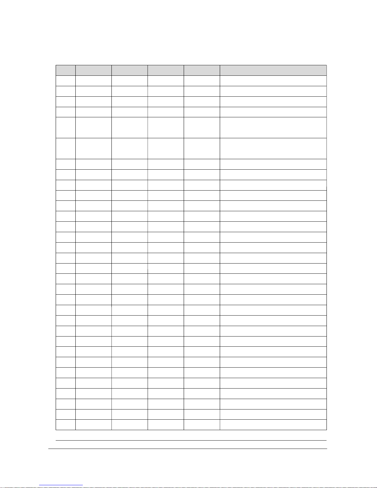
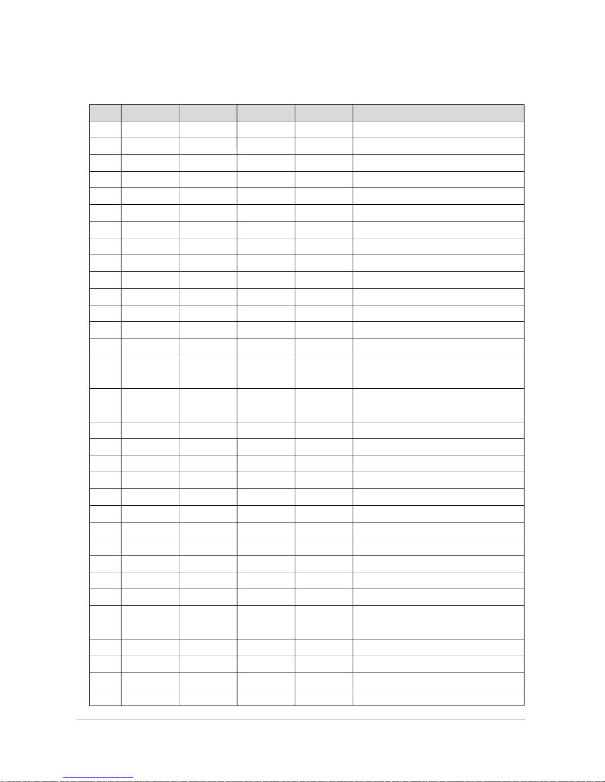
2-2 IC Line Up
IC605
IC606
IC603
IC604
TU01
TUP01
IC804
IC805
IC802
IC803
IC801
ICG01
IC905
IC701
ICS01
IC703
ICS03
IC702
ICS02
IC602
PIC01
IC05
IC06
IC07
IC02
IC13
IC11
IC03
IC04
IC01
MAIN
F-BOX
BP96-00021A
BP96-00022A
AA40-00094A
AA40-00017A
AA40-00095A
AA40-00019A
1203-000203
1203-000203
1203-000293
1203-000298
1203-000165
0801-000314
1103-001274
1001-001073
1001-001114
1002-001193
1001-000223
1001-001113
1201-000407
1204-001658
1002-001045
1204-001372
1204-001550
AA13-00095A
1203-001359
1203-001419
1105-001273
1204-001598
TDA7482
TDA7490
CW SPI MAIN
CS LNA MAIN
CW SUB
CS SUB
SI3050
SI3050
KA7808
KA7809
KA78R12
74HCT86
M24C32
TE6415C
TEA6425
PCF8591
TEA5114
TEA6422
TDA7050
SDA9489
SDA9280
SDA9361
CXA2101AQ
SDP01
1086
4931
KM416S1120
VPC3230
D-CLASS A-AMP MONO
D-CLASS A-AMP 2CH
TCLW3101PD16A(S)
TCLS3101PD09A(S)
TCPW3001PC16A(S)
TCPS3000PC09A(S)
IC-POSI. ADJUST REG.
IC-POSI. ADJUST REG.
IC-POSI. FIXED
IC-POSI. FIXED
IC-POSI. ADJUST
IC-CMOS LOGIC
EEPROM 32K
VIDEO SWITCING
VIDEO S/W
ADC
Analog switch
SOUND S/W
IC-OP AMP
PIP MULTI
DAC, MATRIX
IC-HOR/VER PROCESSOR
IC-VIEO PROCESS
SCAN CONVERTOR
IC POSI. FIXED
IC POSI. FIXED
SDRAM, 10nS
ADC, DEC
Block Des-Loc. Part-Number IC Name Description
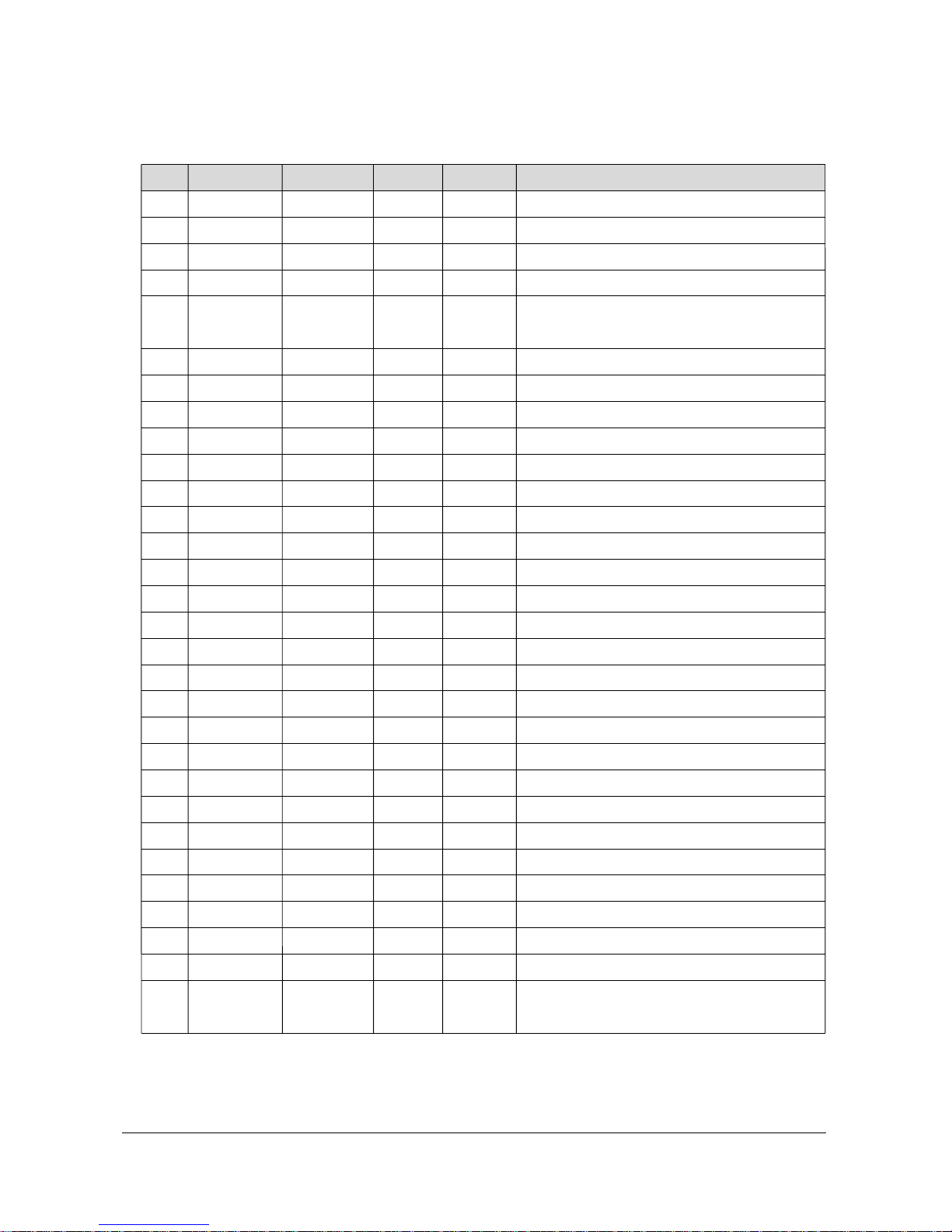
Reference Information
2-4 Samsung Electronics
IC301
IC801S
IC403
Q405
IC803S
QH04
Q403
Q801
Q404
T801S
IC501
IC502
IC503
QF10
QF09
IC504
IC901
IC902
IC903
IC906
IC12
IC02
IC05
IC09
IC01
IC03
IC11
POWER
CRT
MICOM
AC-3
1204-000517
AA96-50364B
1202-000103
0502-001175
AA13-00024A
0502-000442
0505-000156
AA13-20004H
0505-001116
AA26-00186A
AA96-50151B
0502-000153
0502-000131
1201-000010
1204-002000
1102-001126
1105-001305
1203-002470
1204-001910
0904-001615
1205-002191
1204-002017
0801-002518
0903-001290
1203-002648
LA7845
STR-F6658
LM393
2SC5446
TNY253P
2SC4636RB
IRF620
SE135N-LF12
BUZ73A
EER5345
TDA6111Q
2SC2344-D
2SA1011-D
2030
SDA6000(B11)
M27V160
K4S641632
RC1616S25T
MSP4450G
DSP56366
AK4586
NJW1151M
74LCX157
S3P9428
BA33B00
VERTICAL DRIVE
SMPS S-TR
OP-AMP EW DRIVE
HORI. DRIVE TR
IC-HYBRID
TR-POWER
FET-SILICON
IC-HYBRID
HDT DRIVE
MAIN TRANS 160 ~ 300V
R.G.B DRIVE
PUSH-PULL
IC OP AMP
MICOM, TEXT
EPROM 2MByte
SDRAM 64MBit
2.5V REGULATOR
MULTI SOUND PROCESSOR
AC3 PROCESSOR
D/A, SPDIF
VOLUME CONTROL
MULTIPLEXOR
SUB MICOM
3.3V, 1.8V, REG.
Block Des-Loc. Part-Number IC Name Description
Specifications
Samsung Electronics 3-1
3. Specifications
Specifications are subject to change.
Model
Dimensions
(mm)
Weight
Set
Transmitter
Set
Transmitter
Set
Transmitter
WS32Z78R WS32Z9HF
Hi Contrast Instant Reception Type
VHF (CH 1 ~ 12)
UHF (CH 21 ~ 69)
CATV (CH S1 ~ S40)
PAL,SECAM,NTSC4.43, NTSC3.58, PAL60
VHF, UHF: 75 ohm unbalanced type
Video: 38.9 MHz
Sound: (BG)33.4MHz, (I)32.9MHz, (D/K)32.4MHz
Chrominance Subcarrier: 34.47 MHz
AC 110V~230V, 50Hz, 60 Hz
DC 1.5V (AAA Size) x 2
170 W
15 W x 2(Main L/R) /15 W x 2(Surround L/R)
15W(Center)/25W(Woofer)
Transmitter Adjustment: Infrared Rays Type
UHF/VHF electronic tuner fine tuning: Electronic Type
Electronic Function Adjustment
830 (W) x 557 (D) x 619 (H) 829 (W) x 589(D) x 1054 (H)
54 (W) x 31.5 (D) x 220 (H) 54 (W) x 31.5 (D) x 220 (H)
57.8 Kg 82 Kg
153g(including batteries) 153g(including batteries)
Picture Tube
Tuning Ranges
Television System
Antenna Input
Intermediate Frequency
Power Consumption
Sound Output
Adjustment System
Power Supply

3-2 Samsung Electronics
MEMO
Alignment and Adjustments
Samsung Electronics 4-1
4. Alignment and Adjustments
4-1 Adjustments
Usually, a color TV needs only slight touch-up adjustment upon installation. Check the basic
characteristics such as vertical size, horizontal size, and focus. Observe the picture and check for
good black and white details. There must be no objectionable color shading: If color shading is
present, demagnetize the receiver. If color shading persists, re-do purity and convergence adjustments.
Note :
1. This ‘4. Alignment and Adjustments’ applies to S57A chassis applications.
2. AC Power Supply: 100~230 V
3. This service manual has been written on the basis of domestic remote-control model adopting S57A
chassis. Depending on sales location and product specifications, some of specifications herein may
be changed.
S57A contains a dynamic focus circuit. When CRT PCB, FBT or CRT is replaced, be sure to adjust
in the following sequence:
4-1-1 General Alignment Instructions
4-1-2 Focus Adjustment
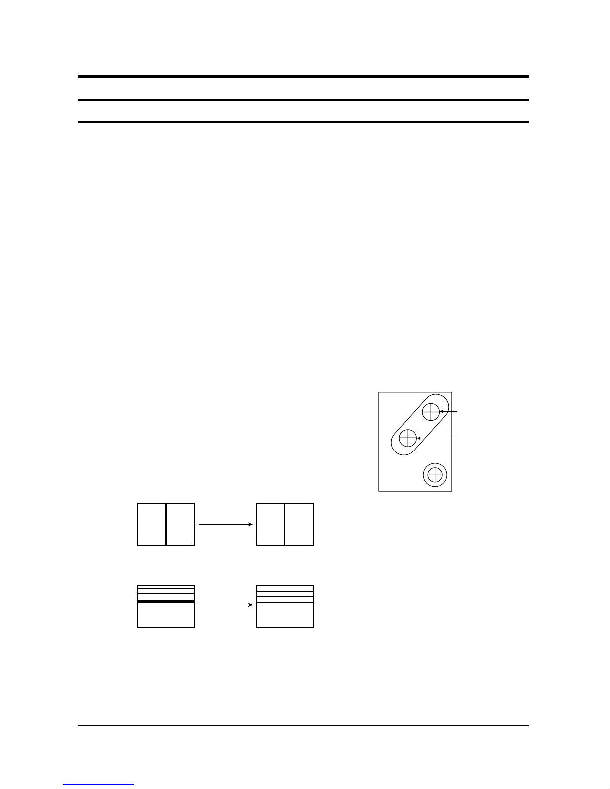
Dynamic Focus Adjustment
1. Input a crosshatch pattern.
2. Select “Standard” from the menu,
3. Turn the Static Focus VR clockwise to set it to its maximum.
4. Turn the Dynamic Focus VR counterclockwise to set it to its
maximum.
5. Turn the Static Focus VR counterclockwise slowly for the clearest
center vertical line.
STATIC FOCUS VR
DYNAMIC FOCUS VR
H
V
NO USE
<FBT FOCUS PACK>
After Adjustment
6. Turn the Dynamic Focus VR clockwise slowly for the clearest third line.
1
2
3
7. Check for the FOCUS of entire screen. If necessary, re-do adjustments 3~6.

Alignment and Adjustments
4-2 Samsung Electronics
4-1-3 Screen Voltage Adjustment
1. Use a DC multi-meter to identify RK, GK, BK. And then adjust FBT Screen VR so that the highest
voltage becomes 175 Vp-p.
4-1-4 White Balance Adjustment
1. Select “Standard” from the menu.
2. Input an 100% White pattern.
3. In standby, press the remote-control keys in the following sequence:
Display Menu,Mute, Power on the TV set.
4. Warm up the TV set at least for 30 minutes.
5. Input a stair signal.
6. Use the Volume +/- buttons on the remote-control to select R Drive,G Drive,B Drive,Sub Cont.
7. Adjust Low-Light while viewing the darker side of screen.
8. Use the Volume +/- buttons on the remote-control to select Rcutoff,Gcutoff,Bcutoff,Sub Brt.
9. Adjust High-Light while viewing the brighter side of screen.
10. If not proper, re-adjust White Balance.
11. Press the Memory button to exit.
4-1-5 Sub-Brightness Adjustment
1. In standby, press the remote-control keys in the following sequence:
Display Menu Mute Power on the TV set.
2. Use the Channel Up/Down buttons to receive the sub bright adjustment signal.
3. Use the Volume +/- buttons to select SBT.
4. Press the Menu or Mute button on the remote control to adjust so that the seventh step on
the right of screen cannot be seen.
5. Press the Memory button to exit.

Alignment and Adjustments
Samsung Electronics 4-3
4-2 MICOM PINNING
P-MQFP-128-2
M2
12345678910111213141516171819202122232425262728293031
32
96959493929190898887868584838281807978777675747372717069686766
65
97
98
99
100
101
102
103
104
105
106
107
108
109
110
111
112
113
114
115
116
117
118
119
120
121
122
123
124
125
126
127
128
64
63
62
61
60
59
58
57
56
55
54
53
52
51
50
49
48
47
46
45
44
43
42
41
40
39
38
37
36
35
34
33
D5
D9
D13
VDD33-5
VSS33-5
D1
D6
D8
D14
D0
D7
VDD33-4
VSS33-4
D15
WR
LDQM
UDQM
RD
CSROM
CLKEN
CSSDRAM
MEMCLK
VDD33-3
VSS33-3
A15/CAS
A14/RAS
A13
A0
A1
A2
A3
A4
P6.1
P6.0
P5.15
P5.14
P3.15
P3.13
P3.12
P3.11
P3.10
VDD25-2
VSS25-2
VDD33-7
VSS33-7
P3.9
P3.8
P3.7
P3.6
P3.5
P3.4
P3.3
P3.2
P3.1
P3.0
RSTIN
D11D3D4
VDD33-6
VSS33-6
D10
D12
D2
TCK
TMS
TDI
TDO
P2.8
P2.9
P2.10
P2.11
P2.12
P2.13
P2.14
P2.14
P2.15
V
SS33-1
VDD33-1
P4.5/CS3
P4.4/A20
P4.3/A19
P4.2/A18
P4.1/A17
VSS25-1
VDD25-1
P4.0/A16
A8A7A6
A5
A10
A11
A12
VSS33-2
VDD33-2
P6.2
P6.3
P6.4
P6.5
P6.6
VSYNC
HSYNC
COR/RSOUT
BLANK/CORBLA
VDD33-8
VSS33-8
XTAL1
XTAL2
VSSA-1
VDDA-1
R
G
B
VSSA-2
VDDA-2
CVBS2
VSSA-3
VDDA-3
CVBS1B
CVBS1A
VSSA-4
VDDA-4
P5.0
P5.1
P5.2
P5.3
TMODE
4-2-1 MICOM PINNING (SDA6001)
Alignment and Adjustments
4-4 Samsung Electronics
4-2-2 MICOM MODULE PIN ALIGNMENT
PIN NO
1
2
3
4
5
6
7
8
9
10
11
12
13
14
15
16
17
PAL MODULE
DVD/DVD2 ID
GND
AV-LINK
5V B+
MAIN-AFT
TTX_CVBS
1080i S/W
TILT
OSD/TTX-F/B
OSD/TTX-R
OSD/TTX-G
OSD/TTX-B
Sub AFT
GND
VS2
HS2
SDA1
PIN NO
19
20
21
22
23
24
25
26
27
28
29
30
31
32
33
34
35
PAL MODULE
SCL1
H/P ID
SDA2
SCL2
BUS STOP/WP
S-MUTE
S-RESET
VGA-ID
STD 5V
GND
KEYS1
KEYS2
IR
LED1
LED2
D-COIL
POWER PORT
Alignment and Adjustments
Samsung Electronics 4-5
4-2-3 MICOM PORT ASSIGNMENT
NO
1
2
3
4
5
6
7
8
9
10
11
12
13
14
15
16
17
18
19
20
21
22
23
24
25
26
27
28
29
30
31
32
33
34
FUNCTION
TCK
TMS
TDI
TDO
P2.8/EXTO IN
P2.9/EXT1 IN
P2.10/EXT2 IN
P2.11/EXT3 IN
P2.12/EXT4 IN
P2.13/EXT5 IN
P2.14/EXT6 IN
P2.15/EXT7 IN
VSS33
VDD33
P4.5/CS3
P4.4/A20
P4.3/A19
P4.2/A18
P4.1/A17
VSS25
VDD25
P4.0/A16
A8
A7
A9
A6
A5
A10
A11
A12
VSS33
VDD33
A4
A3
ASSIGN
TCK
TMS
TDI
TDO
NC
RXD
TXD
5VB CHECK
SW1
SW2
SW3
SW4
DGND
3.3V
CS3
A20
A19
A18
A17
DGND
2.5V
A16
A8
A7
A9
A6
A5
A10
A11
A12
DGND
3.3V
A4
A3
IN/OUT
IN
IN
IN
OUT
IN
OUT
IN
OUT
OUT
OUT
OUT
OUT
OUT
OUT
OUT
OUT
IN/OUT
OUT
OUT
OUT
OUT
OUT
OUT
OUT
OUT
OUT
OUT
ACTIVE H/L
HIGH
HIGH
HIGH
HIGH
LOW
EXPLANATION
CLOCK FOR JTAG INTERFACE
CONTROL SIGNAL FOR JTAG INTERFACE
DATA INPUT FOR JTAG INTERFACE
DATA OUTPUT FOR JTAG INTERFACE
AV-LINK IN/OUT
AV-LINK IN/OUT
SLAVE VCC CHECK POINT
MAIN TUNER SW
MAIN TUNER SW
PIP TUNER SW
PIP TUNER SW
DIGITAL GND FOR PADS
DIGITAL VCC FOR PADS
CHIP SELECT FOR SECOND STATIC MEMORY
EXT MEMORY ADDRESS BIT20
EXT MEMORY ADDRESS BIT19
EXT MEMORY ADDRESS BIT18
EXT MEMORY ADDRESS BIT17
DIGITAL GND FOR DIGITAL CORE
DIGITAL VCC FOR DIGITAL CORE
BOOTSTRAP CONTROL/EXT MEMORY ADDRESS BIT17
EXT MEMORY ADDRESS BIT8
EXT MEMORY ADDRESS BIT7
EXT MEMORY ADDRESS BIT9
EXT MEMORY ADDRESS BIT6
EXT MEMORY ADDRESS BIT5
EXT MEMORY ADDRESS BIT10
EXT MEMORY ADDRESS BIT11
EXT MEMORY ADDRESS BIT12
DIGITAL GND FOR PADS
DIGITAL VCC FOR PADS
EXT MEMORY ADDRESS BIT4
EXT MEMORY ADDRESS BIT3
Alignment and Adjustments
4-6 Samsung Electronics
NO
35
36
37
38
39
40
41
42
43
44
45
46
47
48
49
50
51
52
53
54
55
56
57
58
59
60
61
62
63
64
65
66
FUNCTION
A2
A1
A0
A13
A14/RAS
A15/CAS
VSS33
VDD33
MEMCLK
CSSDRAM
CLKEN
CSROM
RD
UDQM
LDQM
WR
D15
VSS33
VDD33
D7
D0
D14
D8
D6
D1
VSS33
VDD33
D13
D9
D5
D2
D12
ASSIGN
A2
A1
A0
A13
A14/RAS
A15/CAS
DGND
3.3V
CLK-SDRAM
CS-SDRAM
CLK-ENABLE
CS-ROM
RD-ROM
WR-DISABLE
WR-DISABLE
WR
D15
DGND
3.3V
D7
D0
D14
D8
D6
D1
DGND
3.3V
D13
D9
D5
D2
D12
IN/OUT
OUT
OUT
OUT
OUT
OUT
OUT
ACTIVE H/L
-
-
-
-
-
-
-
-
-
-
-
LOW
LOW
LOW
LOW-
-
-
-
-
-
-
-
-
-
-
-
-
-
-
-
-
EXPLANATION
EXT MEMORY ADDRESS BIT2
EXT MEMORY ADDRESS BIT1
EXT MEMORY ADDRESS BIT0
EXT MEMORY ADDRESS BIT13
EXT MEMORY ADDRESS BIT14/ROW ADDRESS
STROBE FOR SDRAM
EXT MEMORY ADDRESS BIT15/COLUMN
ADDRESS STROBE FOR SDRAM
DIGITAL GND FOR PADS
DIGITAL VCC FOR PADS
100MHZ CLOCK FOR SDRAM
CHIP SELECT FOR SDRAM MEMORY
ENABLE FOR SDRAM MEMORY CLOCK
CHIP SELECT FOR ROM
EXTERNAL MEMORY READ STROBE FOR ROM
WRITE DISABLE FOR HIGHBYTE
WRITE DISABLE FOR LOWBYTE
WRITE ENABLE FOR SDRAM
EXT MEMORY DATA BIT15
DIGITAL GND FOR PADS
DIGITAL VCC FOR PADS
EXT MEMORY DATA BIT7
EXT MEMORY DATA BIT0
EXT MEMORY DATA BIT14
EXT MEMORY DATA BIT8
EXT MEMORY DATA BIT6
EXT MEMORY DATA BIT1
DIGITAL GND FOR PADS
DIGITAL VCC FOR PADS
EXT MEMORY DATA BIT13
EXT MEMORY DATA BIT9
EXT MEMORY DATA BIT5
EXT MEMORY DATA BIT2
EXT MEMORY DATA BIT112
Alignment and Adjustments
Samsung Electronics 4-7
NO
67
68
69
70
71
72
73
74
75
76
77
78
79
80
81
82
83
84
85
86
87
88
89
90
91
92
93
94
95
96
97
98
FUNCTION
D10
VSS33
VDD33
D4
D3
D11
RSTIN
P3.0 / SCL0
P3.1 / SDA0
P3.2 / CAPIN
P3.3 / T3OUT
P3.4 / T3EUD
P3.5 / T4IN
P3.6 / T3IN
P3.7 / T2IN
P3.8 / MRST
P3.9 / MTSR
VSS33
VDD33
VSS25
vdd25
P3.10/TXD0
P3.11/RXD0
P3.12/LED1
P3.13/SCLK
P3.15/LED
P5.14/T4EUD
P5.15/T2EUD
P6.0/TRIG_IN
P6.1/TRIG-OUT
P6.2/SDA01
P6.3/SCL01
ASSIGN
D10
DGND
3.3V
D4
D3
D11
RESET
SCL2
SDA2
IR
F/B Switch
POWER S/W
VGA-I/D
BUS STOP/WP
S-RESET
S-MUTE
NC
DGND
3.3V
DGND
2.5V
D-COIL
NC
LED1
LED2
H.P IDENT
NC
S-MUTE
BRK-IN
BRK-OUT
1080i
S/W\SCL1
IN/OUT
-
-
-
-
-
-
IN
IN / OUT
IN / OUT
IN
IN/OUT
OUT
IN
IN
OUT
OUT
-
-
-
-
-
OUT
OUT
OUT
IN
-
OUT
IN
OUT
OUT
IN/OUT
ACTIVE H/L
-
-
-
-
-
-
LOW
-
-
-
LOW
LOW
LOW
LOW
HIGH
-
-
-
-
HIGH
HIGH
HIGH
LOW
-
HIGH
-
HIGH
-
EXPLANATION
EXT MEMORY DATA BIT10
DIGITAL GND FOR PADS
DIGITAL VCC FOR PADS
EXT MEMORY DATA BIT4
EXT MEMORY DATA BIT3
EXT MEMORY DATA BIT11
MICOM HARDWARE RESET
EEPROM CONTROL SERIAL CLOCK LINE
EEPROM CONTROL SERIAL DATA LINE
REMOCON IN
SCART F/B SWITCH
POWER ON/OFF CONTROL
VGA SIGNAL IDENT
IIC STOP & EEPROM WRITE PROTECTION
MSP34XX/DPL3519 & AC3 HARDWARE
RESET CONTROL
MAIN SOUND & HEADPHONE SOUND AMP
MUTE CONTROL
DIGITAL GND FOR PADS
DIGITAL VCC FOR PADS
DIGITAL GND FRO DIGITAL CORE
DITITAL VCC FOR DIGITAL CORE
DEGAUSSING COIL CONTROL
STAND-BY LED CONTROL
TIMER LED CONTROL
IIC STOP/HEADPHONE JACK IDENT
MAIN SOUND & HEADPHONE SOUND AMP
MUTE CONTROL
JTAG BRK IN
JTAG BRK OUT
DVD2/DTV(SCART : DVD)IDENT INPUT
SLAVE IC CONTROL SERIAL CLCOK LINE
Alignment and Adjustments
4-8 Samsung Electronics
NO
99
100
101
102
103
104
105
106
107
108
109
110
111
112
113
114
115
116
117
118
119
120
121
122
123
124
125
126
127
128
FUNCTION
P6.4/SDAI1
P6.5/SCLI1
P6.6/SDA2
VSYNC/VCS
HSYNC
COR/RSOUT
BLANK/CORBLA
VDD33
VSS33
XTAL1
XTAL2
VSSA
VDDA
R
G
B
VSSA
VDDA
CVBS2
VSSA
VDDA
CVBS1B
CVBS1A
VSSA
VDDA
P5.0/AN.0
P5.1/AN.1
P5.2/AN.2
P5.3/AN.3
TMODE
ASSIGN
SDA1
DVD2 ID
NC
V-SYNC
H-SYNC
H/T
OSD-F/B
3.3V
DGND
XTAL-IN
XTAL-OUT
AGND
2.5V
OSD-R
OSD-G
OSD-B
AGND
2.5V
GND
AGND
2.5V
GND
TTX-CVBS
AGND
2.5V
KEY1
KEY2
M-AFT
S-AFT
GND
IN/OUT
IN/OUT
IN
-
IN
IN
OUT
OUT
-
-
IN
OUT
-
IN
OUT
OUT
OUT
-
IN
-
-
IN
-
IN
IN
IN
IN
IN
IN
ACTIVE H/L
-
LOW
-
HIGH
HIGH
HIGH
-
-
-
-
EXPLANATION
SLAVE IC CONTROL SERIAL DATA LINE
DVD2/DTV(SCART/DVD)IDENT INPUT
MAIN PICTURE VERTICAL SYNC IN FOR OSG POSITION
MAIN PICTURE HORIZONTAL SYNC IN FOR OSG
POSITION
HALFTONE SIGNAL OUT(NC)
OSD F/B & HALFTONE SIGNAL OUT
DIGITAL VCC FOR PADS
DIGITAL GND FOR PADS
MICOM CRISTAL OSC IN(6MHz)
MICOM CIRSTAL OSC OUT(6MHz)
ANALOG GND
STD-BY ANALOG POWER
2 LAYER OSG RED OUT
2 LAYER OSG GREEN OUT
2 LAYER OSG BLUE OUT
ANALOG GND
ANALOG POWEER
SET GND WHEN IT IS NOT USED AS CVBS.
ANALOG GND
ANALOG POWER
SET GND TO 75OHM WHEN IT IS NOT USED AS CVBS.
CVBS INPU FOR TELETEXT DECODING
ANALOG GND
ANALOG POWER FOR ADC
VOLUME UP/DOWN, CHANNEL UP/DOWN KEY IN
MENU, TV/VIDEO, NT POWER KEY IN
MAIN TUNER AFT VOLTAGE
SUB TUNER AFT VOLTAGE(NC)
SET GND TO 10KOHM WHEN IT IS USED AS A TEST
MODE PIN IN A NORMAL STATUS.
Alignment and Adjustments
Samsung Electronics 4-9
4-2-4 MICOM FACTORY MODE OPTION BYTE
ITEM OPTION BYTE
00 CRT
01 Language Group
02 Lgnguage
03 ATM
04 Scart/Rca
05 Plug&Play
06 Teleweb
07 CS/CW
08 Lna
09 H/P JACK IDENT
10 TOP TTX
11 High Deviation
12 TTX Group
13 Carrier Mute
14 P . Standard
15 Digital NR
16 Speaker Include?
CIS
Wide
Europe
Russian
On
Scart
On
Off
CS
On
High
Off
Off
Russia
Off
Natural
Off
Europe
Wide
Europe
English
On
Scart
On
On
CW
On
HIgh
Off
Off
W-Europe
Off
Standard
Off
INITIAL
VALUE
Wide
Europe
English
On
Scart
On
Off
CS
On
HIgh
Off
Off
W-Europe
Off
Natural
On
Yes
Remark
-CPT Option(Wide/4:3):P.Size format, WSS Related Option
-User Optional Language Group Setting(Europe/Asia)
-Refer to “Language Group Table”
-Select the language of destination from Language Group
* Note: Countermeasute to prevent IRAN from smuggling Once
Arabic(Persian)has been selected,the user can’t select Persian(Arabic)
-ON: ATM, OFF: Auto search
-SCART: AV-Link,AV Setup Menu, Scart jack switching
-RCA: RCA Jack switching, DVD
-Application of Dolby Prologic((On/Off)
-Dependin on area.(West Europe : On, East Europe : Off)
-CW/CS Tuner switching option
-Application of LNA(Pinp model) (On/Off)
-ON:The main sound is cut off after identigying the headphome jack
-OFF:The headphome jack ident PIN of MICOM is used as an IIC STOP
PIN. The main sound is not cut off
-Set only the countries requesting TOP patent so that TOP TTX
can be available(Countries using TOP:Germany,Austria,Italy,Swiss)
-Solve the Sound Stop problem by tutning High Deviation On for the
countries with SOUND over modulation
-Grouping the TTX Language by Region:Refer to a separate TABLE
-For Italy Only (Option)
-Mode of Picture Statues
-Application of Digital Noise Reduction(On/Off)
-Different by Buyer
Eastern
Europe
Wide
Europe
Country
On
Scart
On
Off
CS
On
High
Off
Off
Refer to TTX Group
Off
Natural
Off
China
Wide
Asia
Chineses
Off
RCA
On
Off
CS
On
High
Off
Off
W-Europe
Off
Natural
Off
Southeast
ASIA
Wide
Asia
Country
Off
RCA
On
Off
CS
On
High
Off
Off
W-Europe
Off
Natural
Off
Refer to Remark

Alignment and Adjustments
4-10 Samsung Electronics
4-3 FACTORY MODE CONTROL
1. Enter & Concel the Factory Mode
1) Usual Remote Control
Enter : PICTURE OFF -> DISPLAY KEY -> MENU KEY -> MUTE KEY
(Press each remote control key with in 3 seconds)
Cannel : POWER OFF -> ON
2) Factory Remote Control
Enter : DISPLAY KEY -> FACTORY KEY
(Press each remote control key with in 3 seconds)
Cannel : POWER OFF -> ON
Press the FACTORY key twice at intervals of at lease 1 second.
(Enter the AGING Mode once)
3) Set Value When Entering the Factory Mode
- Picture Mode & Sound Mode are set to the standard data
- Scan Mode : Natual Scan(NT/PAL All)
- Brigntness : Contrast : 100 Bright : 50 Color : 60
sharpness : 50 Color tone : Center
4) Adjustments
- CH. UP/DOWN Key : Use to select the item you want
- VOLUME UP/DOWN Key : Increases or decreases the value of data.
- MENU Key : Use to save the current set value in EEPROM and exit to the upper mode.
- Use the DIGIT Key to switch channels
- Use the TV/VIDEO Key th conver to the AV Mode
4-3-1 Factroy Mode Data Control
4-4 FACTORY ADJUSTMENT DATA
VIDEO ADJUSTMENT
Y.C-DELAY
DEFLECTION NORMAL
DEFLECTION VGA
DEFLECTION NORMAL[1080i]
DEFLECTION NORMAL[480P]
PICT. IMPROVE [PAL]
PICT. IMPROVE [NTSC]
PICT. IMPROVE [VGA]
PICT. IMPROVE [SECAM]
PICT. IMPROVE [DVD]
PICT. IMPROVE [480P]
PICT. IMPROVE [1080i]
P.STD CHANGE
OPTION BYTE
RESET
Alignment and Adjustments
Samsung Electronics 4-11
VIDEO ADJUSTMENT
Initial Value
32
32
32
8
20
20
20
10
38
11
7
7
8
32
15
7
Resister
CXA2101Q 07HEX(Bit7:2)
CXA2101Q 08HEX(Bit7:2)
CXA2101Q 09HEX(Bit7:2)
CXA2101Q 15HEX(Bit7:2)
CXA2101Q 0AHEX(Bit7:2)
CXA2101Q 0BHEX(Bit7:2)
CXA2101Q 0CHEX(Bit7:2)
CXA2101Q 11HEX(Bit7:4)
CXA2101Q 0DHEX(Bit7:2)
CXA2101Q 11HEX(Bit3:0)
CXA2101Q 03HEX(Bit7:2)
VPC3230 FP28HEX(Bit11:8)
SDA9489X 11HEX(Bit7:4)
SDA9489X 12HEX(Bit7:4)
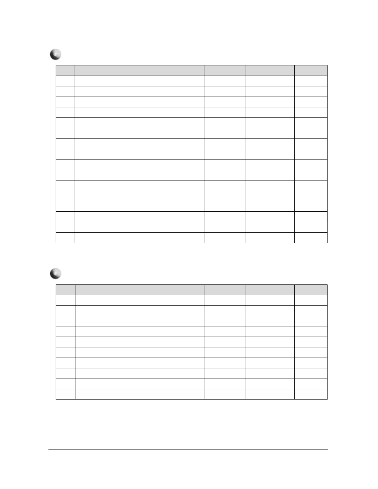
Item
00
01
02
03
04
05
06
07
08
09
10
11
12
13
14
15
OSD
R Drive
B Drive
G Drive
Gamma
R Cutoff
B Cutoff
G Cutoff
Sub Cont
Sub Bri
Sub Color
Sub Tint
V Peaking
Ttx Cont
Ttx Bright
Pip Cont
Pip Bright
Remark
Adjust
Adjust
FIX
FIX
Adjust
Adjust
FIX
Adjust
Adjust
FIX
FIX
FIX
FIX
FIX
FIX
FIX
Range
0 ~ 63
0 ~ 63
0 ~ 63
0 ~ 15
0 ~ 63
0 ~ 63
0 ~ 63
0 ~ 15
0 ~ 63
0 ~ 15
0 ~ 15
0 ~ 12
0 ~ 15
0 ~ 63
0 ~ 15
0 ~ 15
Y.C-DELAY
Resister
SDA9280 03HEX(Bit3:0)
SDA9280 03HEX(Bit3:0)
SDA9280 03HEX(Bit3:0)
SDA9280 03HEX(Bit3:0)
SDA9280 03HEX(Bit3:0)
SDA9280 03HEX(Bit3:0)
SDA9280 03HEX(Bit3:0)
SDA9280 03HEX(Bit3:0)
SDA9280 03HEX(Bit3:0)
SDA9280 03HEX(Bit3:0)
Initial Value
7
9
9
6
7
8
7
4
6
9
Item
00
01
02
03
04
05
06
07
08
09
OSD
PAL-B/G
PAL-D/K/L
PAL-I
SECAM-B/G
SECAM-D/K/L
NTSC
PAL-AV
SECAM-AV
NTSC-AV
DVD
Remark
FIX
FIX
FIX
FIX
FIX
FIX
FIX
FIX
FIX
FIX
Range
0 ~ 15
0 ~ 15
0 ~ 15
0 ~ 15
0 ~ 15
0 ~ 15
0 ~ 15
0 ~ 15
0 ~ 15
0 ~ 15
 Loading...