

Samsung WC-M15i Service Manual
- This Service Manual is a property of Samsung Electronics Co.,Ltd.
Any unauthorized use of Manual can be punished under applicable
International and/or domestic law. -
FACSIMILE
WC-M15i Series
SERVICE
FACSIMILE
MANUAL
Contents
1. Precautions
2. Specifications
3. Circuit Description
4. Disassembly
5. T roubleshooting
6. Exploded Views and Parts List
7. Electrical Parts List
8. Block Diagram
9. Connection Diagram
10. Schematic Diagrams

Precautions
1. Precautions
Follow these safety, ESD, and servicing precautions to prevent personal injury and equipment damage.
1-1 Safety Precautions
1. Be sure that all built-in protective devices are in
place. Restore any missing protective shields.
2. Make sure there are no cabinet openings
through which people- particularly childrenmight insert fingers or objects and contact dangerous voltages.
3. When re-installing chassis and assemblies, be
sure to restore all protective devices, including
control knobs and compartment covers.
4. Design Alteration Warning:Never alter or add to
the mechanical or electrical design of this equipment, such as auxiliary connectors, etc. Such
alterations and modifications will void the manufacturer’s warranty.
5. Components, parts, and wiring that appear to
have overheated or are otherwise damaged
should be replaced with parts which meet the
original specifications. Always determine the
cause of damage or overheating, and correct any
potential hazards.
7. Product Safety Notice:Some electrical and
mechanical parts have special safety-related
characteristics which might not be obvious from
visual inspection. These safety features and the
protection they provide could be lost if a replacement component differs from the original. This
holds true, even though the replacement may be
rated for higher voltage, wattage, etc.
8. Components critical for safety are indicated in
the parts list with symbols .
Use only replacement components that have the
same ratings, especially for flame resistance and
dielectric specifications. A replacement part that
does not have the same safety characteristics as
the original may create shock, fire, or other
safety hazards.
6. Observe the original lead dress, especially near
sharp edges, AC, and high voltage power supplies. Always inspect for pinched, out-of-place,
or frayed wiring. Do not change the spacing
between components and the printed circuit
board.
1-1

Precautions
1-2 ESD Precautions
1. Certain semiconductor devices can be easily
damaged by static electricity. Such components
are commonly called “Electrostatically Sensitive
(ES) Devices”, or ESDs. Examples of typical
ESDs are: integrated circuits, some field effect
transistors, and semiconductor “chip” components.
The techniques outlined below should be followed to help reduce the incidence of component
damage caused by static electricity.
CAUTION : Be sure no po wer is applied to the chassis
or circuit, and observe all other safety precautions.
2. Immediately before handling a semiconductor
component or semiconductor-equipped assembly, drain off any electrostatic charge on your
body by touching a known earth ground. Alternatively, employ a commercially available wrist
strap device, which should be removed for your
personal safety reasons prior to applying power
to the unit under test.
3. After removing an electrical assembly equipped
with ESDs, place the assembly on a conductive
surface, such as aluminum or copper foil, or conductive foam, to prevent electrostatic charge
buildup in the vicinity of the assembly.
4. Use only a grounded tip soldering iron to solder
or desolder ESDs.
Use only an “anti-static” solder removal device.
Some solder removal devices not classified as
“anti-static” can generate electrical charges sufficient to damage ESDs.
5. Do not use Freon-propelled chemicals. When
sprayed, these can generate electrical charges
sufficient to damage ESDs.
6. Do not remove a replacement ESD from its protective packaging until immediately bef ore installing it. Most replacement ESDs are packaged
with all leads shorted together by conductive
foam, aluminum f oil, or a comparable conductive
material.
7. Immediately before removing the protective
shorting material from the leads of a replacement ESD, touch the protective material to the
chassis or circuit assembly into which the device
will be installed.
8. Maintain continuous electrical contact between
the ESD and the assembly into which it will be
installed, until completely plugged or soldered
into the circuit.
9. Minimize bodily motions when handling unpackaged replacement ESDs. Normal motions, such
as the brushing together of clothing fabric and
lifting one’s f oot from a carpeted floor , can generate static electricity sufficient to damage an ESD.
1-3 Super Capacitor or Lithium Battery Precautions
1. Exercise caution when replacing a super capacitor or Lithium battery. There could be a danger of
explosion and subsequent operator injury and/or
equipment damage if incorrectly installed.
2. Be sure to replace the battery with the same or
equivalent type recommended by the manufacturer.
1-2
3. Super capacitor or Lithium batteries contain toxic
substances and should not be opened, crushed,
or burned for disposal.
4. Dispose of used batteries according to the manufacture’s instructions.

Specification
2. Specification
Specifications are correct at the time of printing. Product specifications are subject to change without notice.
See below for product specifications.
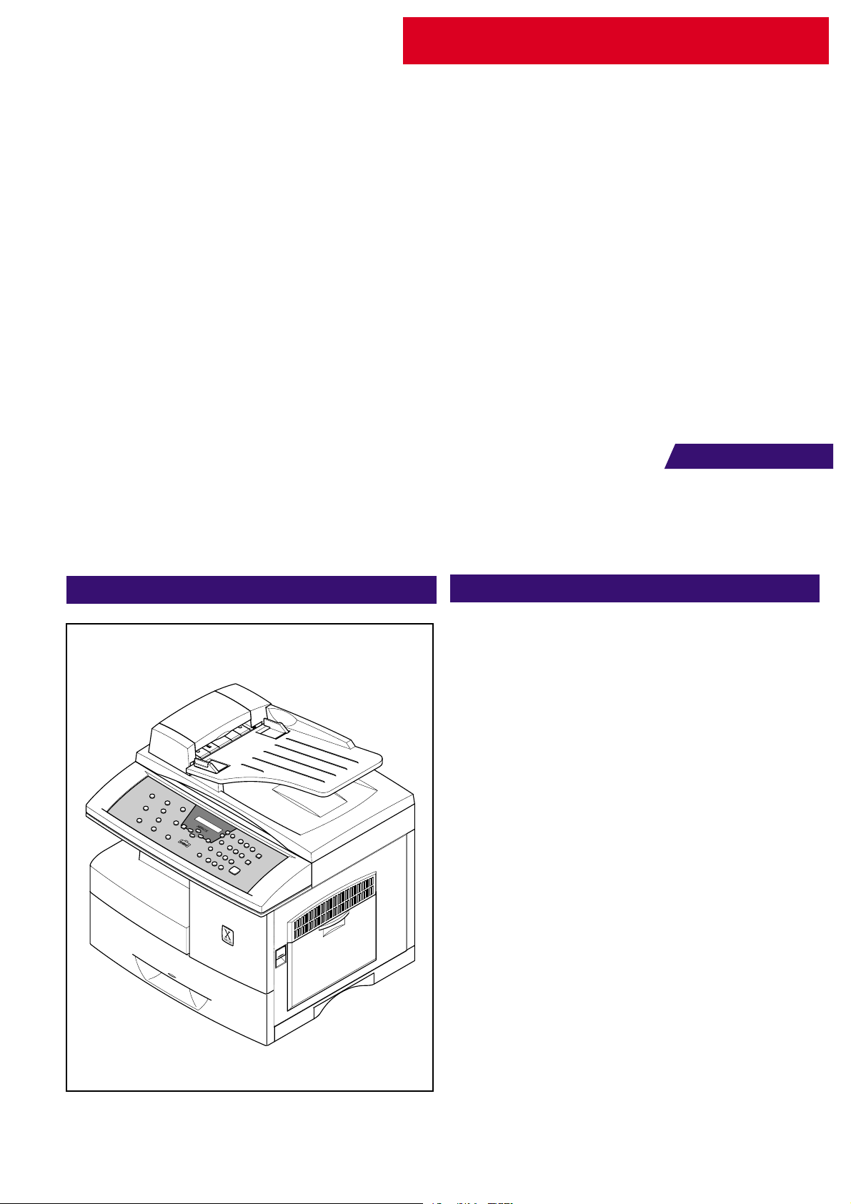
2-1 General Specifications
Item Description
Type of Unit Desktop
Operation System Win95/98/ME/ NT /2000/XP
Duplex Printing Yes(Default)
Interface IEEE1284(ECP)
USB(without HUB mode)
CPU 120 MHz(ARM946ES)
Emulation PCL6
Warming up Time 30 Sec (Stand-By), 25˚C
Absolute Storage Condition Temperature : -20°C ~ 40°C, Humidity : 10% RH ~ 95% RH
Operating Condition Temperature : 10˚C ~ 32˚C, Humidity : 20% RH ~ 80 % RH
Recommended Operating Condition Temperature : 16°C ~ 30°C, Humidity : 30% RH ~ 70% RH
Dimension(W X D X H) 560 X 433 X 459 mm
Weight About 22.5 Kg(with CRU)
* Acoustic Noise Less than 56/50 dB(Copy/Printing mode)
Power Rating AC 100VAC ~ 127VAC ± 15 %, 50/60Hz ± 3Hz
AC 220VAC ~ 240VAC ± 15 % , 50/60Hz ± 3Hz
Power Consumption Avg. 320Wh
Power Save Consumption Avg. 35Wh
Recommended System Requirement Pentium IV 1.2 Ghz, 128 MB RAM, 220MB(Hard Disk)
Minimum System Requirement Pentium II 400Mhz, 64 MB RAM, 120MB(Hard Disk)
LCD 16 characters X 2 lines
Memory 4 Mbyte for flash Memory , 16 Mbyte for SDRAM
* Sound Pressure Level, ISO 7779
Samsung Electronics
2-1

Specification
2-2 Printer Specifications
Item Description
Printing Method Laser Scanning Unit + Electro Photography
*Speed Single Side : Up to 15 PPM
(Letter Size, 5% Character Pattern)
Duplex : Up to 7.5 IPM(Images/Min) (Letter Size, 5% Character Pattern)
Source of Light LSU(Laser Scanning Unit)
Duplex Printing Yes(Default)
Resolution(Horizontal X Vertical) Up to 1200 x 1200 DPI effective output
Feed Method Cassette Type , By Pass Tray,
ADF(Automatic Document Feeder)
Feed Direction FISO(Front-In Side-Out)
Paper Capacity(Input) Cassette : 550 Sheets
By Pass Tray : 100 Sheets(based on 75g/ß
Paper Capacity(Output) Face Down : 250 Sheets
Effective Print Width 203 ± 1mm (8 inch)
* Print speed will be affected by Operating System used, computing performance, application software,
connecting method, media type, media size and job complexity.
≥ , 20lb)
2-3 Facsimile Specification(SCX-5315F Only)
Item Description
Standard Recommendation ITU-T Group3(ITU : International Telecommunications Union)
Application Circuit PSTN or behind PABX
(PSTN : Public Switched Telephone Network.
PABX : Private Automatic Branch Exchange)
Data coding(Compression) MH/MR/MMR/JPEG(Transmission)
Modem speed 33600 /14400/12000/9600/7200/4800/2400 bps
Transmission Speed Approximately 3 sec(33,600 bps)
Effective Scanning Width 8.2 inches(208 mm)
Halftone 256 Levels
Paper Capacity(Input) ADF(Automatic Document Feeder) : 30Sheets(75g/ß
FAX Mode Standard /Fine/Super Fine/Halftone
Memory 4MB
Samsung Electronics2-2
≥ )
2-4 Scanner Specification
Item Description
Type Flatbed(with ADF)
*Speed Mono : Up to 1.2 msec/line, Color : Up to 2.5 msec/line
Device Color CCD(Charge Coupled Device) Module
Interface IEEE1284(ECP Support)
USB(without HUB Mode)
Compatibility TWAIN Standard , WIA
Optical Resolution(H X V) Up to 600 x 600 DPI effective output
Interpolation Resolution Max. 4800 dpi
Halftone 256 Levels
Specification
Effective Scan width 8.2 inches(208 mm)
* Speed will be affected by Operating System used, computing performance, application software, connecting
method, media type, media size and job complexity.
2-5 Copy Specification
Item Description
Mode B/W
Quality Text/Photo/Mixed
Mono Copy Speed
(1)
Optical Resolution (H x V) Up to 600 x 600 DPI effective output
Multi Copy 99 pages
Maximum Original Size Legal
Maximum Page Size Legal
Platen(SDMP) : Up to 12 cpm in A4 size, IDC 5% pattern
ADF (SDMP) : Up to 12 cpm in A4 size, IDC 5% pattern
ADF (MDSP) : Text/mixed : Approx. 7 cpm in A4 size, IDC 5% pattern
: Photo : Approx. 3 cpm in A4 size, IDC 5% pattern
Paper Type Selection Plain , Legal , Cardstock , Transparency
Zoom Range Platen : 25 ~ 400%(1% Step)
ADF : 25~100 %(1% Step)
NOTE :
(1) Speed claims based on the test chart : Letter size.
SDMP : Single Document Multiple Printout
MDSP : Multiple Document Single Printout
• Speed will be affected by Operating System used, computing performance, application software,
connecting method, media type, media size and job complexity.
Samsung Electronics
2-3
Specification
2-6 Telephone Specification(SCX-5315F Only)
Item Description
Speed Dial 80EA
Tone/Pulse Tone only user modeTone/Pulse selectable in tech mode.
2-7 Consumables
Item Description
Type Separate type
(Toner Cartridge / Drum Cartridge)
Life Toner Cartridge Up to 6,000 sheets
( 5% coverage pattern, simplex normal mode )
Drum Cartridge Up to 15,000 sheets
(simplex normal mode )
Samsung Electronics2-4
Circuit Description
3. Circuit Description
3-1 Main PBA
3-1-1 Summary
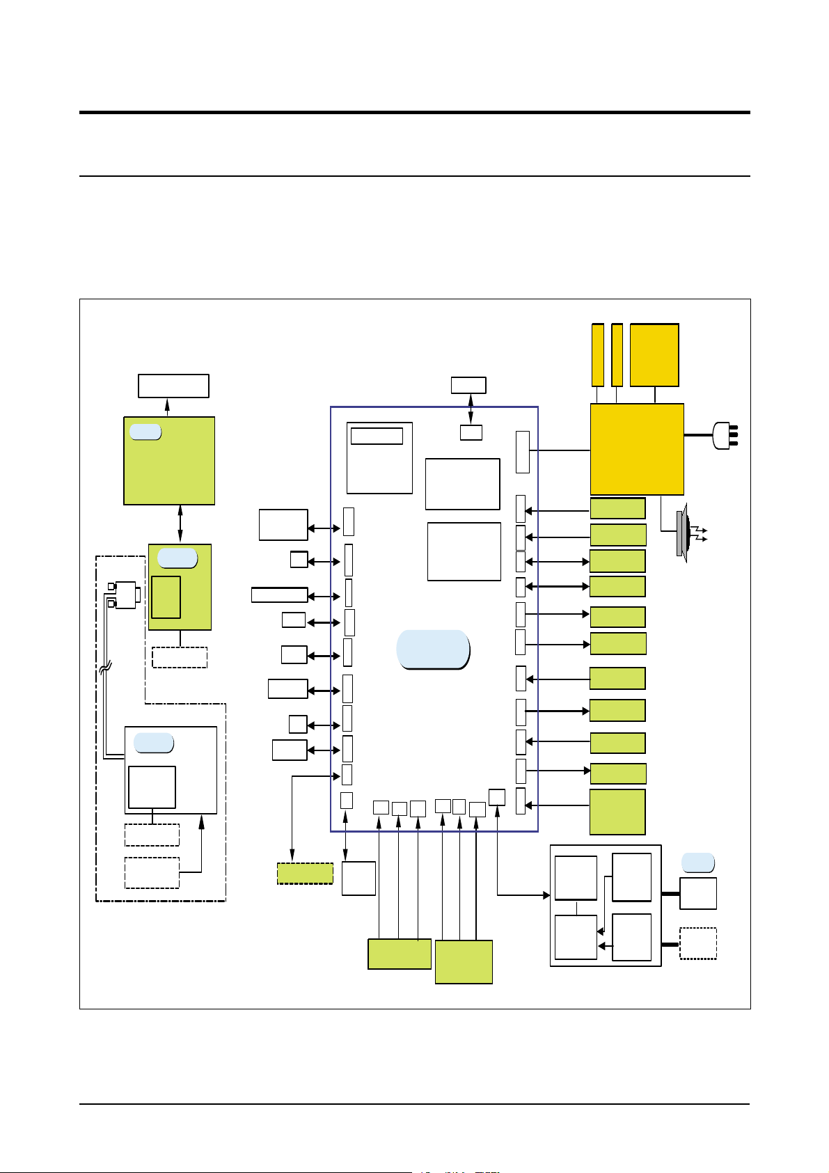
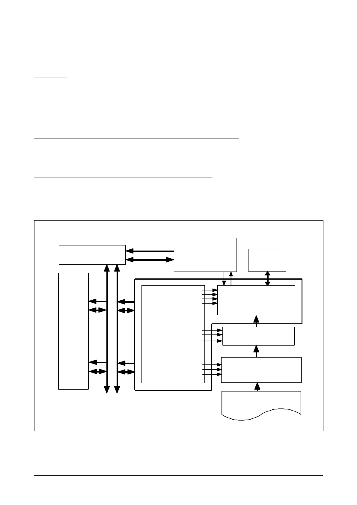
The main circuit that consists of CPU, MFP controller (built-in 32bit RISC processor core: ARM946ES) including various I/O device drivers, system memory, scanner, printer, motor driver, PC I/F, and FAX transceiver controls the whole system. The entire structure of the main circuit is as follows :
M
DEV
SUPPLY
H
V
BLADE
LCD 20x2line
T
H
V
SCAN
OPE
MICOM
- LCD Drive
- Key Scan
5P
Platen
15P D-SUB
D-SUB
CONN.
FLAT MOTOR
Opti o n
ADF
MOTOR
DRIVER
DADF MOTOR
PAPER SENSOR
POS,DET
3P x 2EA
CENTRONICS
CABLE
SCF
OUT BIN FULL
PCNT
HYPER
DEV CNT
OPC
USB CABLE
22P
CCD MODULE
CN8
CN2
C
24P
N
6
Flash DIMM
Net workCARD
C
N
1
36P
6
C
N
8P
3
1
C
N
1
4P
2
C
N
2P
1
9
C
N
2
4P
5
C
N
4P
1
9
C
N
1
2P
7
C
N
4P
1
3
C
N
5
CN1
10P
MAIN PBA
CN2 0 CN24CN3
CN30
CN27
External
Auditron
2P6P2P
2P
(2MB)
PS3
CN15(100 P)
SDRAM DIMM
16MB
CN15(100P)
CN28
3P
3P
CN2 2
C
N
10P
1
4
C
N
8P
3
3
C
11P
N
4
C
N
2P
7
C
N
3P
1
0
C
N
3P
1
1
3P
C
N
1
8
C
3P
N
2
3
C
N
4P
2
1
C
N
2P
2
6
C
N
4P
2
9
TRANSFORMER
4P
1
600/ / 600
SMPS / HVPS
+5V/+24V/+12V/+24Vs/Fuser
DEV M OTOR
FEED MOTOR
LSU
THERMISTOR
FAN1
FAN1
DEV_ID
TONER_TX
TONER_RX
PTL
COVER OPEN
S/W
+24 V / +5V
Tx: Rx
MODEM
EXT_PHONE
SEPRATING
PART
LIU
LINE 1
EXTERNAL
PHONE
INTERFACE
PART
EXTERNAL
PHONE
SOLENOID
PICK_UP,DUPLEX,MP
PAPER
SEN SOR
FEED+P. EMP,EXIT,MP
LINE
INT ERFAC E
<Block Diagram>
3-1

Circuit Description
3-2 Circuit Operation
3-2-1 Clock
1) System Clock
Device Oscillator
Frequency 12MHz
• ARM946ES RISC PROCESSOR: drives PLL internally uses 120MHz and external Bus uses 60 MHz.
2) Video Clock
Device Oscillator
Frequency 57.0167MHz
• Fvd =((PAPER 1SCAN LINE sending time * SCAN effective late /1SCAN LINE DOT #)*4
=(600dpi*600dpi*58.208mm/s*216mm*4)/(25.4mm*25.4mm*76.1%)=28.697MHz
•PAPER 1SCAN LINE sending time=SCAN LINE interval/DOCUMENT SPEED (58.208mm/S)
•1SCAN LINE DOT #=MAZ SCAN distance(216mm)*DOT# per 1mm
3)USB Clock
Device Oscillator
Frequency 48MHz
3-2-2 POWER ON/OFF RESET
1) Signal Operation
Input Signal +3.3V Power Line (VCC)
Output Signal ARM946ES nRESET and 29LU16ø
• POWER ON/OFF DETECT VCC RISING/FALLING 4.5° ≠ 4.6V
RESET TIME (Td) 1.48~1.52ms
• Td=(Ct*V sensing)/I charge (...Ct=33µF, Is=100µA)
2) TIMING CHART
MCLK
nRESET
20 MCLK
nPWRGD
20 MCLK
5.461 ms
(65535 MCLK)
3-2
HICLK
reRESETn
RESETn
CLK falling
5.461 ms
(65535 MCLK)
15 HCLK

Circuit Description
3-2-3 RISC MICROPROCESSOR
1) RISC MICROCESSOR PIN & INTERFACE(SPGPm)
Ball No Pin No Pin Name I/O Description PAD
B1 1 SD15 I/O SDRAM Bus Data[15] BD8TARP_TC
C2 2 VSS_PLL1 - VSS for Core PLL D2 3 VDD_PLL1 - VDD for Core PLL (1.8V) D3 4 DATA0 / GPI1 I/O ROM Bus Data[0] / GPI[1] BD8TRP_FT
E4 5 MCLK I Core PLL Clock Input (12MHz) TLCHT_TC
C1 6 DATA6 / GPI7 I/O ROM Bus Data[6] / GPI[7] BD8TRP_FT
D1 7 DATA1 / GPI2 I/O ROM Bus Data[1] / GPI[2] BD8TRP_FT
E3 8 DATA5 / GPI6 I/O ROM Bus Data[5] / GPI[6] BD8TRP_FT
E2 9 VDD_RING_OSC - VDD for Ring Oscillator (1.8V) E1 10 DATA3 / GPI4 I/O ROM Bus Data[3] / GPI[4] BD8TRP_FT
F3 11 DATA9 / GPI10 I/O ROM Bus Data[9] / GPI[10] BD8TRP_FT
G4 12 GND - GROUND_RING F2 13 DATA8 / GPI9 I/O ROM Bus Data[8] / GPI[9] BD8TRP_FT
F1 14 DATA7 / GPI8 I/O ROM Bus Data[7] / GPI[8] BD8TRP_FT
G3 15 DATA12 / GPI13 I/O ROM Bus Data[12] / GPI[13] BD8TRP_FT
G2 16 DATA11 / GPI12 I/O ROM Bus Data[11] / GPI[12] BD8TRP_FT
G1 17 DATA10 / GPI11 I/O ROM Bus Data[10] / GPI[11] BD8TRP_FT
H3 18 DATA4 / GPI5 I/O ROM Bus Data[4] / GPI[5] BD8TRP_FT
H2 19 DATA15 / GPI16 I/O ROM Bus Data[15] / GPI[16] BD8TRP_FT
H1 20 DATA14 / GPI15 I/O ROM Bus Data[14] / GPI[15] BD8TRP_FT
J4 21 VDD_CORE - VDD for CORE (1.8V) J3 22 DATA19 I/O ROM Bus Data[19] BD8TRP_FT
J2 23 DATA18 I/O ROM Bus Data[18] BD8TRP_FT
J1 24 DATA17 I/O ROM Bus Data[17] BD8TRP_FT
K2 25 DATA16 I/O ROM Bus Data[16] BD8TRP_FT
K3 26 DATA22 I/O ROM Bus Data[22] BD8TRP_FT
K1 27 DATA13 / GPI14 I/O ROM Bus Data[14] / GPI[14] BD8TRP_FT
L1 28 DATA20 I/O ROM Bus Data[20] BD8TRP_FT
L2 29 DATA21 I/O ROM Bus Data[21] BD8TRP_FT
L3 30 DATA25 I/O ROM Bus Data[25] BD8TRP_FT
L4 31 DATA26 I/O ROM Bus Data[26] BD8TRP_FT
M1 32 DATA23 I/O ROM Bus Data[23] BD8TRP_FT
M2 33 DATA24 I/O ROM Bus Data[24] BD8TRP_FT
M3 34 DATA29 I/O ROM Bus Data[29] BD8TRP_FT
M4 35 DATA30 I/O ROM Bus Data[30] BD8TRP_FT
N1 36 DATA27 I/O ROM Bus Data[27] BD8TRP_FT
N2 37 DATA28 I/O ROM Bus Data[28] BD8TRP_FT
N3 38 VDD_ARM - VDD for ARM P1 39 DATA31 I/O ROM Bus Data[31] BD8TRP_FT
P2 40 DATA2 / GPI3 I/O ROM Bus Data[2] / GPI[3] BD8TRP_FT
R1 41 VDD_CORE - VDD for CORE (1.8V) P3 42 nROMCS2 O ROM Bank2 Select_n B4TR_TC
3-3

Circuit Description
Ball No Pin No Pin Name I/O Description PAD
R2 43 nRD O ROM Bus Read_n B4TR_TC
T1 44 nROMCS0 O ROM Bank0 Select_n B4TR_TC
P4 45 nROMCS3 / nIOCS3 /
R3 46 nWR O ROM Bus Write_n B4TR_TC
T2 47 nROMCS1 O ROM Bank1 Select_n B4TR_TC
U1 48 ADDR12 O ROM Bus Addr[12] B8TR_TC
T3 49 ADDR10 O ROM Bus Addr[10] B8TR_TC
U2 50 ADDR13 O ROM Bus Addr[13] B8TR_TC
V1 51 ADDR15 O ROM Bus Addr[15] B8TR_TC
T4 52 ADDR11 O ROM Bus Addr[11] B8TR_TC
U3 53 ADDR14 O ROM Bus Addr[14] B8TR_TC
V2 54 ADDR16 O ROM Bus Addr[16] B8TR_TC
W1 55 ADDR19 I/O ROM Bus Addr[19] BD8TRP_TC
V3 56 ADDR17 I/O ROM Bus Addr[17] BD8TRP_TC
W2 57 ADDR20 I/O ROM Bus Addr[20] BD8TRP_TC
Y1 58 nIOCS0 O IO Bank0 Select_n B4TR_TC
W3 59 ADDR21 I/O ROM Bus Addr[21] BD8TRP_TC
Y2 60 nIOCS1 O IO Bank1 Select_n B4TR_TC
W4 61 ADDR22 I/O ROM Bus Addr[22] BD8TRP_TC
V4 62 ADDR18 I/O ROM Bus Addr[18] BD8TRP_TC
U5 63 ADDR7 O ROM Bus Addr[7] B8TR_TC
Y3 64 VDD_CORE O VDD for CORE (1.8V) Y4 65 nIOCS2 / nDACK0 /
V5 66 ADDR1 O ROM Bus Addr[1] B8TR_TC
W5 67 ADDR8 O ROM Bus Addr[8] B8TR_TC
Y5 68 ADDR9 O ROM Bus Addr[9] B8TR_TC
V6 69 ADDR4 O ROM Bus Addr[4] B8TR_TC
U7 70 ADDR6 O ROM Bus Addr[6] B8TR_TC
W6 71 ADDR2 O ROM Bus Addr[2] B8TR_TC
Y6 72 ADDR3 O ROM Bus Addr[3] B8TR_TC
V7 73 ADDR5 O ROM Bus Addr[5] B8TR_TC
W7 74 VDD_ARM - VDD for ARM Hard Macro(1.8V) -
Y7 75 VDD_CORE - VDD for CORE (1.8V) V8 76 EINT0 / TnRST I Ext. Interrupt0 / TAP Controller
W8 77 EINT1 / TCK I Ext. Interrupt1 / TAP Controller
Y8 78 EINT2 / nRXD2 / TMS I Ext. Interrupt2 / U AR T RX DAT A[2] /
U9 79 EINT3 / nTXD2 / GPO9 I/O Ext. Interrupt3 / UART TX Data[2] /
V9 80 nRxD0 I UART RX Data[0] SCHMITT_FT
W9 81 nRxD1 / GPI17 / TDI I UART RX Data[1] / GPI[17] / TAP
Y9 82 nTxD0 O UART TX Data[0] B4TR_TC
W10 83 TESTMODE I TESTMODE (Nomal : 0) SCHMITT_TC
GPO1
GPO2
O ROM Bank3 Select_n / IO Bank3
Select_n / GPO[1]
O IO Bank2 Select_n / DMA IO Bank0
ACK_n / GPO[2]
Reset_n
Clock
TAP Controller Mode Select
GPO[9]
Controller Data In
B4TR_TC
B4TR_TC
SCHMITT_FT
SCHMITT_FT
SCHMITT_FT
BD4STRP_FT
SCHMITT_FT
3-4

Ball No Pin No Pin Name I/O Description PAD
V10 84 nTxD1 / GPO10 / TDO O UART Tx Data[1] / GPO[10] / Tap
Controller Data Out
Y10 85 TESTSE I TESTSE (Normal : 0) SCHMITT_TC
Y11 86 VDD_CORE - VDD for CORE (1.8V) -
W11 87 RXERR / GPI25 I MAC RX Error / GPI[25] SCHMITT_TC
V11 88 GND - GROUND_RING U11 89 RX_DV / GPI20 O MAC RX Data Valid / GPI[20] SCHMITT_TC
Y12 90 RXD0 / GPI21 O MAC RX Data[0] / GPI[21] SCHMITT_TC
W12 91 nLFPHB1 / nPRINT O Motor Out B_n / Print Start_n B4TR_TC
V12 92 nLFPHB0 / nCMSG O Motor Out B / Command
Message_n
U12 93 nLFPHA0 / CCLK O Motor Out A / Communication Clock B4TR_TC
Y13 94 RXD1 / GPI22 I MAC RX Data[1] / GPI[22] SCHMITT_TC
W13 95 VDO O Video Data Out B8TR_TC
V13 96 SPD / nDREQ3 I/O DIMM Detect / DMA REQ[3]_n BD4SRTP_TC
Y14 97 nWAIT1 / CRS I Wait_n / MAC Carrier Sensor SCHMITT_TC
W14 98 COL / EINT4 I MAC Collision Detect / Ext.
Interrupt4
Y15 99 TX_EN O MAC TX Enable B4TR_TC
V14 100 MDIO I/O MAC Management Data Inout BD4STRUQP_TC
W15 101 TXD3 / GPO14 O MAC TX Data[3] / GPO[14] B4TR_TC
Y16 102 TXD2 / GPO13 O MAC TX Data[2] / GPO[13] B4TR_TC
U14 103 MDC / GPO15 O MAC Management Data Clock /
GPO[15]
V15 104 TXCLK / GPI18 I MAC TX Clock(25MHz) / GPI[18] SCHMITT_TC
W16 105 TXD1 / GPO12 O MAC TX Data[1] / GPO[12] B4TR_TC
Y17 106 PD4 I/O Parallel Port Data[4] BD4STRP_FT
V16 107 TXD0 / nIOCS3 O MAC TX Data[0] / IO Bank3
Select_n
W17 108 RXD3 / GPI24 I MAC RX Data[3] / GPI[24] SCHMITT_TC
Y18 109 PD2 I/O Parallel Port Data[2] BD4STRP_FT
U16 110 PD6 I/O Parallel Port Data[6] BD4STRP_FT
V17 111 RXD2 I MAC RX Data[2] / GPI[23] SCHMITT_TC
W18 112 PWMOUT2 O PWM Output[2] B4TR_TC
Y19 113 VCLK I Video Reference Clock TLCHT_TC
V18 114 RXCLK / GPI19 I MAC RX Clock(25MHz) / GPI[19] SCHMITT_TC
W19 115 PD1 I/O Parallel Port Data[1] BD4STRP_FT
Y20 116 nINIT I Parallel Port Initialization_n SCHMITT_FT
W20 117 VSS_ADC - VSS for ADC -
V19 118 ATEST_OUT O ADC Test Output ANA_TC
U19 119 AIN2 I ADC Channel2 Input ANA_TC
U18 120 AIN1 I ADC Channel1 Input ANA_TC
T17 121 AIN0 I ADC Channel0 Input ANA_TC
V20 122 VDD_ADC - Analog power for ADC (3.3V) U20 123 VDD_CORE - VDD for CORE (1.8V) -
T18 124 GND - GROUND_RING -
T19 125 VDD_CORE - VDD for CORE (1.8V) -
Circuit Description
B4TR_TC
B4TR_TC
SCHMITT_TC
B4TR_TC
B4TR_TC
3-5

Circuit Description
Ball No Pin No Pin Name I/O Description PAD
T20 126 VDD_CORE - VDD for CORE (1.8V) R18 127 VBUS I USB Detect SCHMITT_FT
P17 128 nLREADY / nEBSY I LSU Ready_n / Engine Busy_n SCHMITT_FT
R19 129 nSELECTIN I Parallel Port Select Input_n SCHMITT_FT
R20 130 LSUCLK / nCBSY /
P18 131 PD7 I/O Parallel Port Data[7] BD4STRP_FT
P19 132 PWMOUT1 O PWM Output[1] B4TR_TC
P20 133 PWMOUT0 O PWM Output[0] B4TR_TC
N18 134 nEMSG / nDACK3 /
N19 135 nFSYNC / nLFPHA1 I/O Frame Sync_n / Motor Out A_n BD4STRP_FT
N20 136 nHSYNC I Line Sync_n SCHMITT_FT
M17 137 nSTROBE I Parallel Port Data Strobe_n SCHMITT_FT
M18 138 PD5 I/O Parallel Port Data[5] BD4STRP_FT
M19 139 nWAIT0 / PDE I/O Wait_n / Parallel Port Data Enable BD4STRP_TC
M20 140 nIOCS5 / nSCS4 /
L19 141 PD3 I/O Parallel Port Data[3] BD4STRP_FT
L18 142 nFAULT O Parallel Port Fault_n B4TR_TC
L20 143 nDREQ0 / GPI0 /
K20 144 nRESET I External Reset_n Input SCHMITT_TC
K19 145 PERROR O Parallel Port Paper Error B4TR_TC
K18 146 nAUTOFD I Parallel Port Auto Feed_n SCHMITT_FT
K17 147 nDACK2 / DQM7 /
J20 148 nDREQ2 / DQM6 /
J19 149 nDREQ1 / DQM4 /
J18 150 VDD_CORE - VDD for CORE (1.8V) -
J17 151 nSCS0 O SDRAM Bank0 Select_n BD8TARP_TC
H20 152 nSCS2 O SDRAM Bank2 Select_n BD8TARP_TC
H19 153 nCAS O SDRAM Column Address Select_n BD8TARP_TC
H18 154 nSCS1 O SDRAM Bank1 Select_n BD8TARP_TC
G20 155 nIOCS4 / nSCS3 /
G19 156 BUSY O Parallel Port Busy B4TR_TC
F20 157 PD0 I/O Parallel Port Data[0] BD4STRP_FT
G18 158 SLCT_OUT O Parallel Port Selection Out B4TR_TC
F19 159 nACK O Parallel Port Acknowledge_n B4TR_TC
E20 160 nDACK1 / DQM5 /
G17 161 nRSTOUT / CLKOUT /
F18 162 SA7 O SDRAM Bus Addr[7] BD8TARP_TC
E19 163 SA9 O SDRAM Bus Addr[9] BD8TARP_TC
GPO11
PWMOUT3
GPO3 / TONEOUT
ADDR23
GPO5
GPO6
GPO8
GPO4
GPO7
GPO0
O LSU Clock / Command Busy_n /
GPO[11]
I/O Engine Message_n / DMA
ACK[3]_n / PWM Output[3]
O DRAM Bank4 / IO Bank5 Select_n /
GPO[3] / Tone Pulse Out
I/O DMA REQ[0]_n / GPI[0] / ADDR[23] BD4STRP_TC
O DMA ACK[2]_n / DQM[7] / GPO[5] BD8TARP_TC
I/O DMA REQ[2]_n / DQM[6] / GPO[6] BD8TARP_TC
I/O DMA REQ[1]_n / DQM[4] / GPO[8] BD8TARP_TC
O IO Bank4 / SDRAM Bank3 Select_n
/ GPO[4]
O DMA ACK[1]_n / DQM[5] / GPO[7] BD8TARP_TC
O Internal Reset_n Out / Internal Sys-
tem Clock Out / GPO[0]
B4TR_TC
BD4STRP_FT
BD8TARP_TC
BD8TARP_TC
B8TR_TC
3-6

Ball No Pin No Pin Name I/O Description PAD
D20 164 VDD_USB - VDD for USB Hard Macro (1.8V) E18 165 SA10 O SDRAM Bus Addr[10] BD8TARP_TC
D19 166 SA12 O SDRAM Bus Addr[120 BD8TARP_TC
C20 167 BA0 O SDRAM Bus Bank Select Addr[0] BD8TARP_TC
E17 168 nRAS O SDRAM Row Address Select_n BD8TARP_TC
D18 169 DQM2 O SDRAM Bus DQM[2] BD8TARP_TC
C19 170 DQM1 O SDRAM Bus DQM[1] BD8TARP_TC
B20 171 BA1 O SDRAM Bus Bank Select Addr[1] BD8TARP_TC
C18 172 DQM0 O SDRAM Bus DQM[0] BD8TARP_TC
B19 173 DQM3 O SDRAM Bus DQM[3] BD8TARP_TC
A20 174 RREF I/O USB PHY Register Reference ANA_FT
A19 175 VSSL - VSS for Deserialisation Flip flops B18 176 VDDL - VDD for Deserialisation Flip flops
(1.8V)
B17 177 VSSB - VSS for buffers C17 178 DMNS I/O USB2 DATA- ANA_FT
D16 179 DPLS I/O USB2 DATA+ ANA_FT
A18 180 VDD3_USB - VDD for USB1.1 FS compliance
(3.3V)
A17 181 VSSC - VSS for DLL and Xor tree C16 182 VDDC - VDD for DLL and Xor tree (1.8V) B16 183 VDDB - VDD for buffers (1.8V) A16 184 VDD_USB - VDD for USB Hard Macro (1.8V) C15 185 UCLK I USB PLL Input Clock (12MHz) TLCHT_TC
D14 186 VSS_PLL2 - VSS for USB PLL B15 187 VDD_PLL2 - VSS for USB PLL (1.8V) A15 188 SA11 O SDRAM Bus Addr[11] BD8TARP_TC
C14 189 SA6 O SDRAM Bus Addr[6] BD8TARP_TC
B14 190 SA5 O SDRAM Bus Addr[5] BD8TARP_TC
A14 191 SA8 O SDRAM Bus Addr[8] BD8TARP_TC
C13 192 SA3 O SDRAM Bus Addr[3] BD8TARP_TC
B13 193 SA2 O SDRAM Bus Addr[2] BD8TARP_TC
A13 194 SA4 O SDRAM Bus Addr[4] BD8TARP_TC
D12 195 SA0 O SDRAM Bus Addr[0] BD8TARP_TC
C12 196 SA1 O SDRAM Bus Addr[1] BD8TARP_TC
B12 197 CKE O SDRAM Clock Enable BD8TARP_TC
A12 198 nWE O SDRAM Write Enable_n BD8TARP_TC
B11 199 SD30 I/O SDRAM Bus Data[30] BD8TARP_TC
C11 200 SD31 I/O SDRAM Bus Data[31] BD8TARP_TC
A11 201 SD29 I/O SDRAM Bus Data[29] BD8TARP_TC
A10 202 SD25 I/O SDRAM Bus Data[25] BD8TARP_TC
B10 203 SD26 I/O SDRAM Bus Data[26] BD8TARP_TC
C10 204 SD27 I/O SDRAM Bus Data[27] BD8TARP_TC
D10 205 SD28 I/O SDRAM Bus Data[28] BD8TARP_TC
A9 206 SD21 I/O SDRAM Bus Data[21] BD8TARP_TC
B9 207 SD22 I/O SDRAM Bus Data[22] BD8TARP_TC
Circuit Description
-
-
3-7

Circuit Description
Ball No Pin No Pin Name I/O Description PAD
C9 208 SD23 I/O SDRAM Bus Data[23] BD8TARP_TC
D9 209 SD24 I/O SDRAM Bus Data[24] BD8TARP_TC
A8 210 SD18 I/O SDRAM Bus Data[18] BD8TARP_TC
B8 211 SDCLK0 O SDRAM Clock Output0 BD8TARP_TC
C8 212 SD20 I/O SDRAM Bus Data[20] BD8TARP_TC
A7 213 SD14 I/O SDRAM Bus Data[14] BD8TARP_TC
B7 214 SD19 I/O SDRAM Bus Data[19] BD8TARP_TC
A6 215 SD11 I/O SDRAM Bus Data[11] BD8TARP_TC
C7 216 SD16 I/O SDRAM Bus Data[16] BD8TARP_TC
B6 217 SDCLK1 O SDRAM Clock Output1 BD8TARP_TC
A5 218 SD12 I/O SDRAM Bus Data[12] BD8TARP_TC
D7 219 SD17 I/O SDRAM Bus Data[17] BD8TARP_TC
C6 220 SD13 I/O SDRAM Bus Data[13] BD8TARP_TC
B5 221 SD8 I/O SDRAM Bus Data[8] BD8TARP_TC
A4 222 SD5 I/O SDRAM Bus Data[5] BD8TARP_TC
C5 223 SD9 I/O SDRAM Bus Data[9] BD8TARP_TC
B4 224 SD6 I/O SDRAM Bus Data[6] BD8TARP_TC
A3 225 SD3 I/O SDRAM Bus Data[3] BD8TARP_TC
D5 226 SD10 I/O SDRAM Bus Data[10] BD8TARP_TC
C4 227 SD7 I/O SDRAM Bus Data[7] BD8TARP_TC
B3 228 SD4 I/O SDRAM Bus Data[4] BD8TARP_TC
B2 229 SD1 I/O SDRAM Bus Data[1] BD8TARP_TC
A2 230 SD0 I/O SDRAM Bus Data[0] BD8TARP_TC
C3 231 SD2 I/O SDRAM Bus Data[2] BD8TARP_TC
3-8

Circuit Description
2) RISC MICROCESSOR PIN & INTERFACE(CIP4)
No Pin Name I/O Description P ad Type Current drive
1 GND2 P Vss Supply vss2i 2 NTEST I Nand Tree Test Mode Selection pticd 3 TM I Global Test Mode Selection pticd 4 TEST1 I Test Mode Selection 1 pticd 5 GND17 P Vss Supply vss3op 6 TEST2 I Test Mode Selection 2 pticd 7 XDACK1 I DMA Acknowledge Signal 1 ptis 8 XDREQ1 O DMA Request Signal 1 phob4 4mA
9 VDD1 P Vdd Supply vdd2i -
10 XDACK2 I DMA Acknowledge Signal 2 ptis 11 XDREQ2 O DMA Request Signal 2 phob4 4mA
12 XDACK3 I DMA Acknowledge Signal 3 ptis 13 XDREQ3 O DMA Request Signal 3 phob4 4mA
14 nRESET I Global Reset ptis 15 CLK_OUT O PLL Clock Out phob12 12mA
16 GND3 P Vss Supply vss2i 17 XP I Clock Oscillation Input phsoscm26 10~40MHz
18 XPOUT O Clock Oscillation Output phsoscm26 10~40MHz
19 GNDD16 P Vss Supply vss2t_abb 20 FILTER* O PLL Filter Pump Out poar50_abb 21 GND1 P Vss Supply vbb_abb 22 VDDA9,VDDD9 P Vdd Supply vdd2t_abb 23 GND24,GND33 P Vss Supply vss3t_abb 24 RTC_XO O RTC Clock Oscillation Output poar50_abb 25 RTC_XI I RTC Clock Oscillation Input piar50_abb 26 VDD8,VDD18 P Vdd Supply vdd3t_abb 27 IRQ O Interrupt Request Signal phob4 4mA
28 nCS I CIP4 Chip Select ptis 29 GND4 P Vss Supply vss2i 30 nRD I CIP4 CPU Read Control ptis 31 nWR I CIP4 CPU Write Control ptis 32 BA1 I Bank Address Bus [1] ptis 33 BA0 I Bank Address Bus [0] ptis 34 GND19 P Vss Supply vss3op 35 A5 I CPU Address Bus [5] ptis 36 A4 I CPU Address Bus [4] ptis 37 A3 I CPU Address Bus [3] ptis 38 VDD2 P Vdd Supply vdd2i 39 A2 I CPU Address Bus [2] ptis 40 A1 I CPU Address Bus [1] ptis 41 A0 I CPU Address Bus [0] ptis 42 GND5 P Vss Supply vss2i 43 D31 B CPU Data Bus [31] phbst8 8mA
3-9

Circuit Description
No Pin Name I/O Description Pad Type Current drive
44 D30 B CPU Data Bus [30] phbst8 8mA
45 D29 B CPU Data Bus [29] phbst8 8mA
46 D28 B CPU Data Bus [28] phbst8 8mA
47 GND20 P Vss Supply vss3op 48 D27 B CPU Data Bus [27] phbst8 8mA
49 D26 B CPU Data Bus [26] phbst8 8mA
50 D25 B CPU Data Bus [25] phbst8 8mA
51 VDD11 P Vdd Supply vdd3op 52 D24 B CPU Data Bus [24] phbst8 8mA
53 D23 B CPU Data Bus [23] phbst8 8mA
54 D22 B CPU Data Bus [22] phbst8 8mA
55 D21 B CPU Data Bus [21] phbst8 8mA
56 GND6 P Vss Supply vss2i 57 D20 B CPU Data Bus [20] phbst8 8mA
58 D19 B CPU Data Bus [19] phbst8 8mA
59 D18 B CPU Data Bus [18] phbst8 8mA
60 GND21 P Vss Supply vss3op 61 D17 B CPU Data Bus [17] phbst8 8mA
62 D16 B CPU Data Bus [16] phbst8 8mA
63 D15 B CPU Data Bus [15] phbst8 8mA
64 D14 B CPU Data Bus [14] phbst8 8mA
65 VDD3 P Vdd Supply vdd2i 66 D13 B CPU Data Bus [13] phbst8 8mA
67 D12 B CPU Data Bus [12] phbst8 8mA
68 D11 B CPU Data Bus [11] phbst8 8mA
69 GND7 P Vss Supply vss2i 70 D10 B CPU Data Bus [10] phbst8 8mA
71 D9 B CPU Data Bus [9] phbst8 8mA
72 D8 B CPU Data Bus [8] phbst8 8mA
73 D7 B CPU Data Bus [7] phbst8 8mA
74 GND22 P Vss Supply vss3op 75 D6 B CPU Data Bus [6] phbst8 8mA
76 D5 B CPU Data Bus [5] phbst8 8mA
77 D4 B CPU Data Bus [4] phbst8 8mA
78 VDD12 P Vdd Supply vdd3op 79 D3 B CPU Data Bus [3] phbst8 8mA
80 D2 B CPU Data Bus [2] phbst8 8mA
81 D1 B CPU Data Bus [1] phbst8 8mA
82 D0 B CPU Data Bus [0] phbst8 8mA
83 GND8 P Vss Supply vss2i 84 TX_EN1 O Motor Control Tx Enable 1 phob4 4mA
85 TX_EN2 O Motor Control Tx Enable 2 phob4 4mA
86 TX_A O Motor Control Tx Channel A phob4 4mA
87 TX_B O Motor Control Tx Channel B phob4 4mA
88 GND23 P Vss Supply vss3op -
3-10

No Pin Name I/O Description Pad Type Current drive
89 nTX_A O Motor Control Tx Channel A phob4 4mA
90 nTX_B O Motor Control Tx Channel A phob4 4mA
91 MOTOR_POL I Motor Polarity ptis 4mA
92 VDD4 P Vdd Supply vdd2i 93 PItg1 O CIS/CCD PItg1 Signal phob8 8mA
94 PI1 O CIS/CCD PI1 Signal phob8 8mA
95 PI2 O CIS/CCD PI2 Signal phob8 8mA
96 GND9 P Vss Supply vss2i 97 PIrs O CIS/CCD PIrs Signal phob8 8mA
98 PIcp O CIS/CCD PIsh Signal phob8 8mA
99 ADC_CLK O AFE ADC Clock phob8 8mA
100 VDD13 P Vdd Supply vdd3op 101 CDS2_CLK O AFE CDS2 Clock phob8 8mA
102 SCLK1 O AFE SIO Sync. Clock phob8 8mA
103 SLOAD1 O AFE SIO Read/Write Control Signal phob8 8mA
104 VDD10 P Vdd Supply vdd3op 105 SDO1 O AFE SIO Serial Output 1 phob8 8mA
106 SDIO1 B AFE SIO Serial Inout/Output 1 phbst8 8mA
107 SDIO2 B AFE SIO Serial Inout/Output 2 phbst8 8mA
108 GND10 P Vss Supply vss2i 109 AFE_D9 I A/D Converted Data Bus [9] ptis 110 AFE_D8 I A/D Converted Data Bus [8] ptis 111 AFE_D7 I A/D Converted Data Bus [7] ptis 112 AFE_D6 I A/D Converted Data Bus [6] ptis 113 VDD5 P Vdd Supply vdd2i 114 AFE_D5 I A/D Converted Data Bus [5] ptis 115 AFE_D4 I A/D Converted Data Bus [4] ptis 116 AFE_D3 I A/D Converted Data Bus [3] ptis 117 GND25 P Vss Supply vss3op 118 AFE_D2 I A/D Converted Data Bus [2] ptis 119 AFE_D1 I A/D Converted Data Bus [1] ptis 120 AFE_D0 I A/D Converted Data Bus [0] ptis 121 GND11 P Vss Supply vss2i 122 SRAM_A15 O SRAM Address Bus [15] phob8 8mA
123 SRAM_A14 O SRAM Address Bus [14] phob8 8mA
124 SRAM_A13 O SRAM Address Bus [13] phob8 8mA
125 SRAM_A12 O SRAM Address Bus [12] phob8 8mA
126 VDD14 P Vdd Supply vdd3op 127 SRAM_A11 O SRAM Address Bus [11] phob8 8mA
128 SRAM_A10 O SRAM Address Bus [10] phob8 8mA
129 SRAM_A9 O SRAM Address Bus [9] phob8 8mA
130 GND26 P Vss Supply vss3op 131 SRAM_A8 O SRAM Address Bus [9] phob8 8mA
132 SRAM_A7 O SRAM Address Bus [9] phob8 8mA
133 SRAM_A6 O SRAM Address Bus [9] phob8 8mA
Circuit Description
3-11

Circuit Description
No Pin Name I/O Description Pad Type Current drive
134 SRAM_A5 O SRAM Address Bus [9] phob8 8mA
135 GND12 P Vss Supply vss2i 136 SRAM_A4 O SRAM Address Bus [9] phob8 8mA
137 SRAM_A3 O SRAM Address Bus [9] phob8 8mA
138 SRAM_A2 O SRAM Address Bus [9] phob8 8mA
139 SRAM_A1 O SRAM Address Bus [9] phob8 8mA
140 VDD6 P Vdd Supply vdd2i 141 SRAM_A0 O SRAM Address Bus [9] phob8 8mA
142 SRAM_nWR O SRAM Write Enable Signal phob8 8mA
143 SRAM_D15 B SRAM Data Bus [15] phbst8 8mA
144 SRAM_D14 B SRAM Data Bus [14] phbst8 8mA
145 GND27 P Vss Supply vss3op 146 SRAM_D13 B SRAM Data Bus [13] phbst8 8mA
147 SRAM_D12 B SRAM Data Bus [12] phbst8 8mA
148 SRAM_D11 B SRAM Data Bus [11] phbst8 8mA
149 GND13 P Vss Supply vss2i 150 SRAM_D10 B SRAM Data Bus [10] phbst8 8mA
151 SRAM_D9 B SRAM Data Bus [9] phbst8 8mA
152 SRAM_D8 B SRAM Data Bus [8] phbst8 8mA
153 SRAM_D7 B SRAM Data Bus [7] phbst8 8mA
154 VDD15 P Vdd Supply vdd3op 155 SRAM_D6 B SRAM Data Bus [6] phbst8 8mA
156 SRAM_D5 B SRAM Data Bus [5] phbst8 8mA
157 SRAM_D4 B SRAM Data Bus [4] phbst8 8mA
158 GND28 P Vss Supply vss3op 159 SRAM_D3 B SRAM Data Bus [3] phbst8 8mA
160 SRAM_D2 B SRAM Data Bus [2] phbst8 8mA
161 SRAM_D1 B SRAM Data Bus [1] phbst8 8mA
162 SRAM_D0 B SRAM Data Bus [0] phbst8 8mA
163 GND14 P Vss Supply vss2i 164 GPO7/PItg2 O General Purpose Output [7] phob8 8mA
165 GPO6/RLED O General Purpose Output [6] phob8 8mA
166 GPO5/GLED O General Purpose Output [5] phob8 8mA
167 GPO4/BLED O General Purpose Output [4] phob8 8mA
168 VDD7 P Vdd Supply vdd2i 169 GPO3/PItg3 O General Purpose Output [3] phob8 8mA
170 GPO2/PIsh O General Purpose Output [2] phob8 8mA
171 GPO1/
LEVEL_SHIFT
172 GPO0 O General Purpose Output [0] phob8 8mA
173 GND29 P Vss Supply vss3op 8mA
174 GPIO2B/AFE_D11 B General Purpose Input/Output 2 [11] phbst8 8mA
175 GPIO2A/AFE_D10 B General Purpose Input/Output 2 [10] phbst8 176 GPIO29/AFE_D9 B General Purpose Input/Output 2 [9] phbst8 8mA
177 GND30 P Vss Supply vss3op 8mA
178 GPIO28/AFE_D8 B General Purpose Input/Output 2 [8] phbst8 8mA
O General Purpose Output [1] phob8 8mA
3-12

No Pin Name I/O Description Pad Type Current drive
179 GPIO27/AFE_D7 B General Purpose Input/Output 2 [7] phbst8 8mA
180 GPIO26/AFE_D6 B General Purpose Input/Output 2 [6] phbst8 181 GPIO25/AFE_D5 B General Purpose Input/Output 2 [5] phbst8 8mA
182 VDD16 P Vdd Supply vdd3op 8mA
183 GPIO24/AFE_D4 B General Purpose Input/Output 2 [4] phbst8 8mA
184 GPIO23/AFE_D3 B General Purpose Input/Output 2 [3] phbst8 8mA
185 GPIO22/AFE_D2 B General Purpose Input/Output 2 [2] phbst8 8mA
186 GND15 P Vss Supply vss2i 8mA
187 GPIO21/AFE_D1 B General Purpose Input/Output 2 [1] phbst8 8mA
188 GPIO20/AFE_D0 B General Purpose Input/Output 2 [0] phbst8 8mA
189 GPIO1F/
SRAM_D15
190 GPIO1E/
SRAM_D14
191 GND31 P Vss Supply vss3op 8mA
192 GPIO1D/
SRAM_D13
193 GPIO1C/
SRAM_D12
194 GPIO1B/
SRAM_D11
195 GPIO1A/
SRAM_D10
196 VDD17 P Vdd Supply vdd3op
197 GPIO19/SRAM_D9 B General Purpose Input/Output 1 [9] phbst8
198 GPIO18/SRAM_D8 B General Purpose Input/Output 1 [8] phbst8
199 GPIO17/SRAM_D7 B General Purpose Input/Output 1 [7] phbst8
200 GND32 P Vss Supply vss3op
201 GPIO16/SRAM_D6 B General Purpose Input/Output 1 [6] phbst8 202 GPIO15/SRAM_D5 B General Purpose Input/Output 1 [5 phbst8 203 GPIO14/SRAM_D4 B General Purpose Input/Output 1 [4] phbst8 204 GPIO13/SRAM_D3 B General Purpose Input/Output 1 [3] phbst8 205 GND18 P Vss Supply vss3op 206 GPIO12/SRAM_D2 B General Purpose Input/Output 1 [2] phbst8 207 GPIO11/SRAM_D1 B General Purpose Input/Output 1 [1] phbst8 208 GPIO10/SRAM_D0 B General Purpose Input/Output 1 [0] phbst8 -
B General Purpose Input/Output 1 [15] phbst8 8mA
B General Purpose Input/Output 1 [14] phbst8 -
B General Purpose Input/Output 1 [13] phbst8 8mA
B General Purpose Input/Output 1 [12] phbst8 -
B General Purpose Input/Output 1 [11] phbst8 4mA
B General Purpose Input/Output 1 [10] phbst8 -
Circuit Description
3-13

Circuit Description
3-2-4 PROGRAM ROM (FLASH MEMORY) CONTROL
1) DEVICE
TYPE No.
CAPACITY
AM29LU160DB
4 MBYTE (1MB * 16BITS * 2)
2) PROGRAMMING
BEFORE ASS’Y
AFTER ASS’Y
EPROM PROGRAMMER or PROGRAMMING at the factory
DOWNLOAD from PC
3) OPERATING PRINCIPLE
When the RCSO(ROM CHIP SELECT)signal is activated from the CPU after the POWER is ON, it activates RD SIGNAL and reads the DATA(HIGH/LOW) stored in the FLASH MEMORY to control the over all system. The FLASH MEMORY may also write. When turning the power on, press and hold the key(power
switch) for 2 - 3 seconds, then the LED will scroll and the PROGRAM DOWNLOAD MODE will be activated.
In this mode, you can download the program through the parallel port.
AC CHARACTERISTICS
Read Status Data (last two cycles)
PA
Addresses
Program Command Sequence (last two cycles)
t
WC
555h
t
AS
PA PA
t
AH
CE#
OE#
t
WP
WE#
Data
RY/BY#
V
t
VCS
CC
t
CS
t
DS
t
DH
A0h
Notes:
1. PA = program address, PD = program data, D
2. Illustration shows device in word mode.
Figure 17. Program Operation Timings
CE#
WE#
BYTE
t
CH
t
WPH
PD
t
BUSY
is the true data at the program address.
OUT
The falling edge of the last WE# signal
t
SET
(tAS)
t
HOLD
t
WHWH1
(tAH)
Status
D
OUT
t
RB
Note: Refer to the Erase/Program Operations table for tAS and tAH specifications.
Figure 16. BYTE# Timings for Write Operations
3-14

3-2-5 DRAM CONTROL
1) DEVICE
Circuit Description
TYPE NO.
CAPACITY
2) OPERATING PRINCIPLE
DRAM can either read or write. The data can be stored in the DRAM only when the power is on. It stores
data white the CPU processes data. The address to read and write the data is specified by RAS SIGNAL
and CAS SIGNAL. DRAMWE*SIGNAL is activ ated when writing data and DRAMOE*SIGNAL, when reading. You can expand up to 64MBYTE of DRAM in this system.
Start Address ~ End Address Contents
0x00000000 ~ 0x00FFFFFF ROM Bank0
0x01000000 ~ 0x01FFFFFF ROM Bank1
0x02000000 ~ 0x02FFFFFF ROM Bank2
0x03000000 ~ 0x03FFFFFF ROM Bank3
0x04000000 ~ 0x0FFFFFFF Unused
0x10000000 ~ 0x1FFFFFFF Special Function Registers
0x20000000 ~ 0x20FFFFFF I/O Bank0
0x21000000 ~ 0x21FFFFFF I/O Bank1
0x22000000 ~ 0x22FFFFFF I/O Bank2
0x23000000 ~ 0x23FFFFFF I/O Bank3
0x24000000 ~ 0x24FFFFFF I/O Bank4
0x25000000 ~ 0x25FFFFFF I/O Bank5
0x26000000 ~ 0x26FFFFFF DMA I/O Bank0
0x27000000 ~ 0x27FFFFFF DMA I/O Bank1
0x28000000 ~ 0x28FFFFFF DMA I/O Bank2
0x29800000 ~ 0x29FFFFFF DMA I/O Bank3
0x2A000000 ~ 0x2FFFFFFF Unused
0x30000000 ~ 0x30FFFFFF RSH SRAM
0x31000000 ~ 0x31FFFFFF HPVC SRAM
0x32000000 ~ 0x32FFFFFF MOTOR SRAM
0x33000000 ~ 0x37FFFFFF Unused
0x38000000 ~ 0x38FFFFFF USB CSR & FIFO
0x39000000 ~ 0x390003FF USB PLUG DETECT
0x38000500 ~ 0x3FFFFFFF Unused
0x40000000 ~ 0x4FFFFFFF SDRAM array0 (bank 0)
0x50000000 ~ 0x5FFFFFFF SDRAM array1 (bank 1)
0x60000000 ~ 0x6FFFFFFF SDRAM array2 (bank 2)
0x70000000 ~ 0x7FFFFFFF SDRAM array3 (bank 3)
0x80000000 ~ 0xBFFFFFFF SDRAM array0~4 (Mirror)
0xC0000000 ~ 0xC00007FF MAC
0xC0000800 ~ 0xC0FFFFFF Unused
K4S
16MBYTES (1M * 16BITS * 4Bank * 2)
3-15

Circuit Description
3-2-5-1 SDRAM DRAM read timing
Basically the Extended Data Out DRAM is similar to Fast Page Mode DRAM. For FPM, the data are v alid only
when the nCAS is active while reading the internal data, however, it has a latch that the data will be
continuously outputted even after the nCAS is inactivated.
While configuring the software, you must set the timing register of SFR considering the clock speed and the
DRAM spec.
0 1 2 3 4 5 6 7 8 9 10 11 12 13 14 15 16 17 1 8 19
CLOCK
A10/AP
DQ
CKE
CS
RAS
CAS
ADDR
BA
BA
CL=2
CL=3
HIGH
*Note 1
*Note 2
RAa RBb CAa RCc CBb RDd CCc CDd
0
1
RAa RBb RCc RDd
QAa0 QAa1 QAa2 QBb0 QBb1 QBb2 QCc0 QCc1 QCc2 QDd0 QDd1 QDd2
QAa0 QAa1 QAa2 QBb0 QBb1 QBb2 QCc0 QCc1 QCc2 QDd0 QDd1 QDd2
WE
DQM
Row Active
(A-Bank)
(A-Bank)
Row Active
(B-Bank)
Read
(B-Bank)
Row Acive
(C-Bank)
Read
Precharge
(A-Bank)
(C-Bank)
(D-Bank)
Read
Precharge
(B-Bank)
Read
(D-Bank)
Precharge
(D-Bank)
Precharge
(C-Bank)
: Don't care
* Note : 1. CS can be don’t cared when RAS, CAS and WE are hih at the clock high going dege.
2. To interrupt a burst read by row precharge, both the read and the precharge banks must be the
same.
3-16
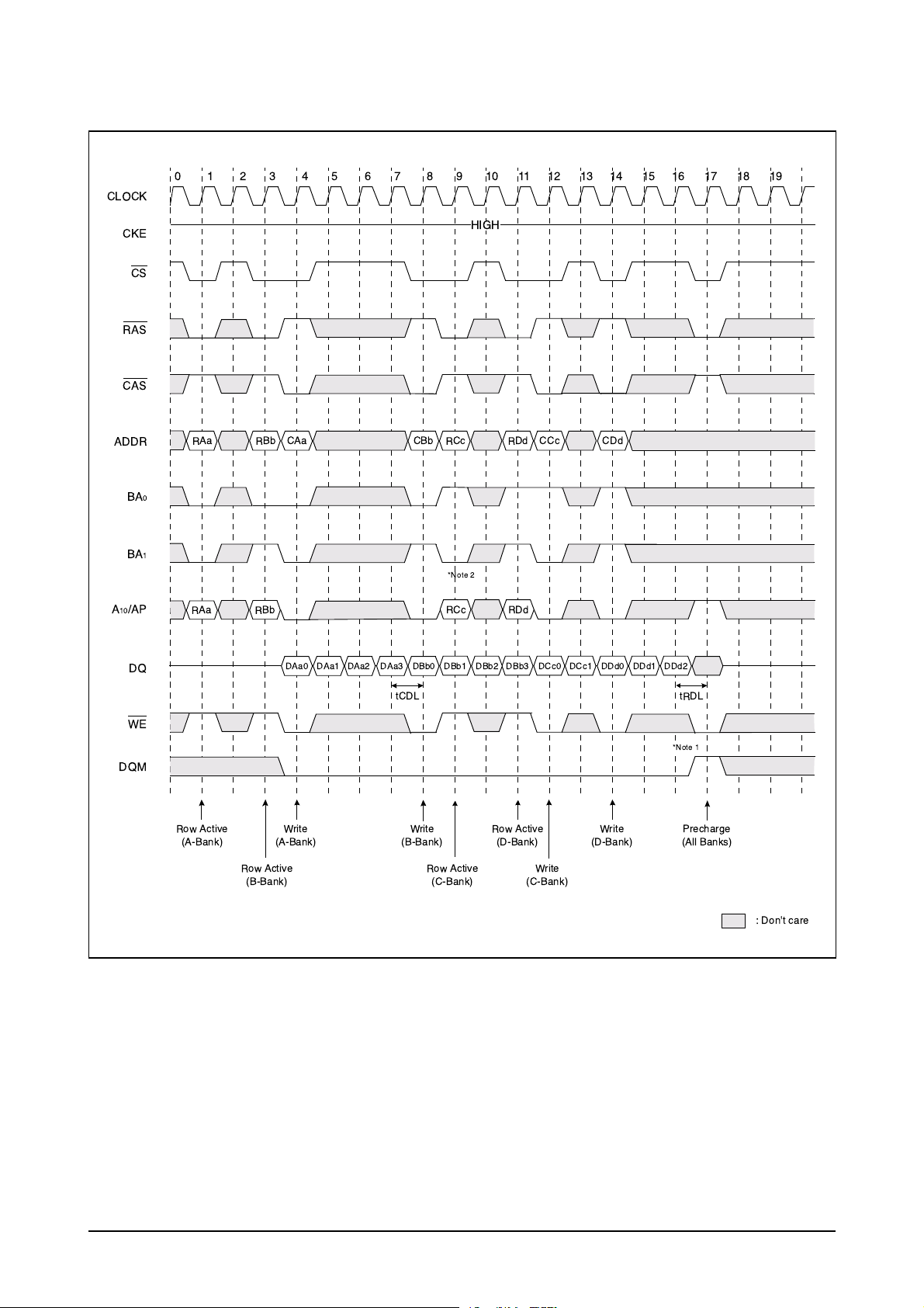
3-2-5-2 SDRAM write timing
012345678910111213141516171819
CLOCK
Circuit Description
CKE
RAS
CAS
ADDR
BA
BA
A
10
/AP
DQ
CS
HIGH
RAa RBb CAa CBb RCc RDd CCc CDd
0
1
*Note 2
RAa RBb
DAa0 DAa1 DAa2 DAa3 DBb0 DBb1 DBb2 DBb3 DCc0 DCc1 DDd0 DDd1 DDd2
RCc RDd
tCDL
tRDL
WE
*Note 1
DQM
Row Active
(A-Bank)
(A-Bank)
Row Active
(B-Bank)
Write
Write
(B-Bank)
Row Active
(C-Bank)
Row Active
(D-Bank)
(C-Bank)
Write
Write
(D-Bank)
Precharge
(All Banks)
: Don't care
*Note : 1. To interrupt burst write by Row precharge, DQM should be asserted to mask invalid input data.
2. To interrupt burst wrige by Row precharge, both the write and the prechargebanks must be the
same.
3-17

Circuit Description
3-2-6 FS781 (FREQUENCY ATTENUATOR)
This system used FS741 for the main clock for EMI SUPPRESSION.
It spreads the source clock in a consistent bandwidth to disperse the energy gathered in order to attenuate
the energy.
The capacitor value of the loop filter(PIN 4) is set depending on the source clock used or the spread bandwidth. Refer to FS781 Spec. for detail.
3-2-7 USB (Universal Serial Bus)
NS’s USBN9602 is used as the interface IC and 48MHz clock is used.
When the data is received through the USB port, EIRQ1 SIGNAL is activated to send interrupt to CPU,
then it directly sends the data to DRAM by IOCS4*&DRAMA(11) SIGNAL through DRAMD (24;31).
3-2-8 SRAM : 1MByte SRAM K6F1008U2C
It stores a variety of option data.
3-2-9 FAX Transceiver
3-2-9-1. GENERAL
This circuit processes transmission signals of modem and between LIU and modem.
3-2-9-2. modem (u44)
FM336 is a single ship fax modem. It has functions of DTMF detection and DTMF signal production as well as
functioins of modem. TX A1, 2 is transmission output port and RX IN is received data input port. / POR signal
controlled by MFP controller (U3:ARM946ES) can initialize modem (/M_RST) without turning off the system.
D0-D7 are 8-bit data buses. RS0-RS4 signals to select the register in modem chips. /RS and /WR signals control READ and WRITE respectively. /IRQ is a signal for modem interrupt.
Transmission speed of FM336 is supported up to 33.6k.
The modem is connected to LINE through transformer directly.
3-18
< FAX TRANSCEIVER >

Circuit Description
3-3 Scanner
3-3-1 SUMMARY
This flat-bed type device to read manuscripts has 600dpi CCD as an image sensor. There is one optical sensor for detecting CCD home position and Scan-end position. The home position is detected by a optical sensor which is attached to the CCD Module. The Scan-end position is calculated by numer of motor step.
CCD
Charge Coupled Device improves productivity and allows a compact design.
This machine uses a color CCD.
• Minimum Scan Line Time for One Color : 2.5mSec
• Light Source Power : +18V
• Maximum Pixel frequency : 10MHz
• Effective Sensor Element : 5340 X 3
• Clamp Level : 0.7~ 0.8V
• Bright Output : MIN 0.8V
IRQ
AIN
ADC_REF T
12-bit
A
/D convert er
AFE_CIP4
Interrupt
Control
CPU I/F
Module
ADC_REFB
SRAM
1024x8
(R/G/ B)
SRAM
8192x8
(2line)
PI_TG
PI1
Sensor
Interfac e
Gamma
Correction
Enlargemen t
/Reduction
Vp eak
Contro l
CIP4
Register
PI2
Shadi ng
Correction
EXT SRAM
Shading
Acquisitio n
Imag e
Proces s ing
Module
DMA
Interfac e
Vertical
Decimation
SRAM
256x8
SRAM
4096x16
(2 line)
Motor
Con trol
SRAM
1024x8
SRA M_A[ 15:0]
SRA M_D[15:0]
SRA M_nRD
SRA M_nWR
TX_A, B
nTX_ A, B
TX_EN1, EN2
A[5:0] D [15:0]nCS nRD nWR nXDREQ nXDACK
<Block Diagram>
3-19

Circuit Description
3-3-2 Key Features
view
Over
(1) 0.5µm C-MOS process(TLM), 208-PIN QFP, STD85 library
(2) Frequency : Max PLL 80 MHz
(3) On-Chip oscillator
(4) Method : Raster scanning method
(5) Image Sauce : 300/400/600dpi CIS & CCD
(6) Scanning Mode
• color gray image: each 8 bits / RGB
• mono gray image: 8 bits / pixel
• binary image: 1 bit / pixel (for text/phoot/mixed mode)
(7) Maximum scanning width : A3, 600dpi (8K effective pixels)
(8) Ideal MSLT (A4, 600/300dpi)
• color gray image: 3x5Kx80nsec = 1.2msec (7/28 CPM)
• mono gray image: 1x5Kx80nsec = 0.4msec (21/84 CPM)
• binary image: 1x5Kx80nsec = 0.4msec (21/84 CPM)
(9) A/D conversion depth : 12bits
Pixel processing structure
• Minimum pixel processing time : 4 system clocks
• High speed pipelined processing method
(Shading correction, Gamma correction, Enlargement/Reducement, and Binarization)
Shading Correction
(1) White shading correction support for each R/G/B
(2) White shading data memory : 3x8Kx12bits = 288Kbits 384Kbits (external)
(3) Black shading data memory : 3x8Kx12bits = 288Kbits 384Kbits (external)
Gamma Correction
(1) Independent Gamma table for each RGB component
(2) Gamma table data memory : 3x1Kx8bits = 24Kbits (internal)
Binarization (mono)
(1) 256 Gray’s halftone representation for Photo document : 3x5 EDF(Error DifFusion) method proposed by
Stucki.
(2) LAT(Local Adaptive Thresholding) for Text document :
• use of 5x5 LOCAL WINDOW (TIP ALGORITHM)
• ABC(Automatic Background Control) :Tmin Automatic change
(3) Mixed mode processing for text/photo mixed document
(4) EDF data memory : 2x4Kx16bits = 128Kbits (internal)
(5) LAT data memory : 4x4Kx16bits = 256Kbits (external)
Scaling of input image
(1) Scaling factor
• Horizontal direction: 25 ~ 800% by 1% unit
• Vertical direction: 25 ~ 100% by 1% unit
(2) Scaling data memory : 2x8Kx8bits = 128Kbits (internal)
3-20
Circuit Description
Intelligent scan motor controlloer
(1) Automatic acceleration/deceleration/uniform velocity
(2) Data memory : 256x16bits = 4Kbits (internal)
Auto-Run
Automatic CLK_LINE (line processing start control) and •’TG (line scan start control) signal generation|
(1)Available resynchronization of øTG signal
(2) programmable øTG’s period & CLK_LINE’s occurrence number
Processed data output format in DTM(Data Transfer Module)
(1)DMA mode : Burst/On-demand mode
(2) CDIP I/F : LINE_SYNC, PIXEL_SYSNC, PIXEL_DATA[7:0]
36 General Purpose Input/Output : 8(GPO), 28(GPIO)
Black/White reversion, and Image Mirroring support
DATA MEMORY
CPU
SPGPm
ADD R- BUS ADDR- BUS
DAT A- BUS
ADDR BU S
DATA BUS
Scan/Motor
Driver
DATA- BUS
DMA Controller
(SPGPm
CLK_LINE
CLK_PIX
LINE_PERIOD
IW IN
ADC_CLK
CDS2_CLK
AFE Contro l
Signal
PI_TG
PI1 , PI2
Tx_A, Tx_B,
nTx_A, nTx_B
)
T
T
R
R
D
D
M
M
A
A
_
_
R
A
E
C
Q
K
1M bit
SRAM
Image
Processor
AFE
12b i t A DC
12bit (R/ G/ B)
Analog Sign al
Scanner
CIP4
DOCUMENT IMAGE
<External interfce with CIP4>
3-21

Circuit Description
AIN
ADC_REF T
12-bit
A
/D converter
AFE_CIP4
1024x8
(R/G/B)
8192x8
ADC_REFB
SRAM
SRAM
( 2line)
PI_TG
PI1
Sensor
Interface
Gamma
Correctio n
Enlargemen t
/Reduct ion
PI2
Shadi ng
Correction
EXT SRAM
Shading
Acquisition
Imag e
Proces sing
Module
Vertical
Decimation
SRAM_A[ 15:0]
SRAM_D[15:0]
SRAM_nRD
SRAM_nWR
SRAM
256x8
SRAM
4096x16
(2 line)
IRQ
Int errupt
Control
CPU I/F
Module
Vp eak
Control
DMA
CIP4
Interface
Register
A[5:0] D[15:0]nCS nRD nWR nXDREQ nXDACK
<Block diagram of CIP4>
Motor
Con trol
SRAM
1024x8
TX_A, B
nTX_ A, B
TX_EN1, EN2
3-22

Circuit Description
3-4 HOST INTERFACE:
Referred to IEEE 1284 standard.
3-4-1. Host Interface
PARALLEL PORT INTERFACE PART ARM946ES has the Parallel Port Interface Part that enables Parallel
Interface with PC. This part is connected to PC through Centronics connector. It generates major control
signals that are used to actuate parallel communication. It is comprised of/ERROR, PE, BUSY, /ACK,
SLCT, /INIT, /SLCTIN, /AUTOFD and /STB. This part and the PC data transmission method support the
method specified in IEEE P1283 Parallel Port Standard (http://www.fapo.com/ieee1284.html). In other
words, it supports both compatibility mode (basic print data transmitting method), the nibble mode
(4bit data; supports data uploading to PC) and ECP (enhanced capabilities port: 8bits data - high speed
two-way data transmission with PC). Compatibility mode is generally referred to as the Centronics mode
and this is the protocol used by most PC to transmit data to the printer. ECP mode is an improved protocol for the communication between PC and peripherals such as printer and scanner, and it provides
high speed two-way data communication. ECP mode provides two cycles in the two-way data transmission; data cycle and command cycle. The command cycle has two formats; Run-Length Count and Channel Addressing. RLE (Run-Length Count) has high compression rate (64x) and it allows real-time data
compression that it is useful for the printer and scanner that need to transmit large raster image that has a
series of same data. Channel Addressing was designed to address multiple devices with single structure. For example, like this system, when the fax/printer/scanner have one structure, the parallel port can be
used for other purposes while the printer image is being processed.This system uses RLE for high speed
data transmission. PC control signals and data send/receive tasks such as PC data printing, high speed
uploading of scanned data to PC, upload/download of the fax data to send or receive and monitoring the system control signal and overall system from PC are all processed through this part.
PPD(7: 0)
BUSY
nSTROBE
nAC
K
DATA
<Compatibility Hardware Handshaking Timing>
3-23
 Loading...