

Samsung UP1500 800-A1, UP1500 User Manual

UP1500
User’s Manual
Part Number: UP1500 800-A1

UP1500 User’s Manual
© 2001 Samsung Electronics Co., Ltd. All rights reserved.
Part #: UP1500 800-A1
Date: May 09, 2001
Samsung Electronics Co., Ltd.
San #24 Nongseo-Ri, Kiheung-Eup
Yongin-City, Kyunggi-Do, KOREA
Tel: 82-31-209-3282
Samsung Electronics Co., Ltd. reserves the right to make changes in its products without notice in
order to impro ve design or performance char acteristics.
This document is considered to be preliminary with further revisions and corrections in process.
Samsung Electronics Co., Ltd. makes no representations or warranties with respect to the accuracy or
completeness of the conte nts of t his pu bli catio n or th e info rma tion co nta in ed h e re in, and rese rve th e
right to make changes at any time, without notice. Samsung Electronics Samsung Electronics Co., Ltd.
disclaims responsibility for any consequences resulting from the use of the information included in
this publication.
This publication neither states nor implies any representations or warranties of any kind, including
but not limited to, any implied warranty of merchanta bility or fitness for a particula r purpose. Samsung
Electronics Co., Ltd. products are not authorized for use as critical components in life support devices
or systems without Alpha Processor, Inc.’s written approval.Sa msun g El ectroni cs Co., L td. assumes
no liability whatsoever for claims associated with the sale or use (including the use of engineering
samples) of Samsung Electronics Co., Ltd. products except as provided in Samsung Electronics Co.,
Ltd.’s Terms and Conditions of Sale for such products.
Trademarks
AMD-761 System Controller is a trademark of AMD.
Other product names used in this publication are for identification purposes only and may be
trademarks of their respective companies.
Preliminary Product Information
The information in this publication is preliminary, and is believed to be accurate at the time of
publication. Samsung Elec tronics Co., Ltd. makes no representations or warra nties with respect to the
accuracy or completeness of the contents of this pu blication or th e information c ontained he rein, and
reserves the right to make changes at any time, without notice.
UP1500 800-A1 ii

UP1500 User’s Manual Revision History
Revision History
Date Rev Description
03/12/01
UP1500
800-A1
UP1500 User’s Manual first product release. This document supports the
UP1500 800-A product.
UP1500 800-A1 iii

UP1500 User’s Manual Table of Contents
Table of Contents
Revision History iii
Table of Contents iv
List of Figures vi
List of Tables vii
Preface ix
Chapter 1 UP1500 Introduction 1-1
1.1 Features . . . . . . . . . . . . . . . . . . . . 1-1
1.2 System Components . . . . . . . . . . . . . . . . 1-2
Chapter 2 System Configuration 2-1
2.1 Board Layout and Components. . . . . . . . . . . . . 2-1
2.2 Memory Subsystem . . . . . . . . . . . . . . . . 2-3
2.2.1 Memory Configuration. . . . . . . . . . . . . . . 2-3
2.2.2 Memory Guidelines . . . . . . . . . . . . . . . 2-4
2.3 Configuration Settings . . . . . . . . . . . . . . . 2-5
2.3.1 Firmware Image Selection . . . . . . . . . . . . . 2-5
2.3.2 System Bus Speed Selection . . . . . . . . . . . . 2-6
2.3.3 Cache Size Selection . . . . . . . . . . . . . . . 2-6
2.4 Initialization Strapping . . . . . . . . . . . . . . . 2-7
2.4.1 System Clock Speed . . . . . . . . . . . . . . . 2-7
2.4.2 Disable Divider . . . . . . . . . . . . . . . . 2-7
2.4.3 Inclk Delay Enable . . . . . . . . . . . . . . . 2-7
2.4.4 CPU Clk Hist . . . . . . . . . . . . . . . . . 2-7
2.4.5 AGP Clk MUX . . . . . . . . . . . . . . . . 2-7
2.4.6 Physical S2K Length. . . . . . . . . . . . . . . 2-8
2.4.7 Outclk Delay Enable . . . . . . . . . . . . . . . 2-8
2.4.8 CPU Div 0 . . . . . . . . . . . . . . . . . . 2-8
Chapter 3 Electrical, Environmental and Physical Data 3-1
3.1 Power Specifications . . . . . . . . . . . . . . . . 3-1
3.1.1 Power Consumption . . . . . . . . . . . . . . . 3-1
3.1.2 Power Supply . . . . . . . . . . . . . . . . . 3-1
3.1.3 Power Connector . . . . . . . . . . . . . . . . 3-2
UP1500 800-A1 iv

UP1500 User’s Manual Table of Contents
3.2 Environmental Specifications . . . . . . . . . . . . . 3-2
3.2.1 Cerification. . . . . . . . . . . . . . . . . . 3-3
3.2.2 Thermal . . . . . . . . . . . . . . . . . . . 3-4
3.3 Enclosure Requirements . . . . . . . . . . . . . . . 3-6
3.4 Physical Parameters . . . . . . . . . . . . . . . . 3-6
3.4.1 UP1500 Parameters . . . . . . . . . . . . . . . 3-6
3.4.2 UP1500 Mounting Hole Specification . . . . . . . . . 3-6
3.5 Rear Panel I/O Shield . . . . . . . . . . . . . . 3-7
Chapter 4 Software Support 4-1
4.1 Software Overview . . . . . . . . . . . . . . . . 4-1
4.1.1 FSB . . . . . . . . . . . . . . . . . . . . 4-1
4.1.2 Reset PALcode . . . . . . . . . . . . . . . . 4-1
4.1.3 Alpha SRM Console . . . . . . . . . . . . . . . 4-1
4.1.4 Operating System . . . . . . . . . . . . . . . . 4-2
4.2 Alpha SRM Console . . . . . . . . . . . . . . . . 4-2
4.2.1 Invoking the SRM Console . . . . . . . . . . . . . 4-2
4.2.2 Command Summary . . . . . . . . . . . . . . . 4-3
4.2.3 Displaying the System Configurations . . . . . . . . . 4-6
4.2.4 Setting the System date . . . . . . . . . . . . . . 4-10
4.2.5 Booting the Operating System . . . . . . . . . . . . 4-11
4.2.6 Updating Firmware (SRM Console) . . . . . . . . . . 4-12
4.2.7 Using Environment Variables . . . . . . . . . . . . 4-13
4.2.8 Environment Variable Summary . . . . . . . . . . . 4-15
4.2.9 Finding Help . . . . . . . . . . . . . . . . . 4-23
4.3 FSB . . . . . . . . . . . . . . . . . . . . . 4-24
Chapter 5 Troubleshooting 5-1
5.1 Hardware Startup . . . . . . . . . . . . . . . . . 5-1
5.1.1 No Video Present . . . . . . . . . . . . . . . . 5-1
5.1.2 LED Status Indicators . . . . . . . . . . . . . . 5-1
5.1.3 Beep Code . . . . . . . . . . . . . . . . . . 5-2
5.2 Error Recovery Procedures . . . . . . . . . . . . . . 5-3
5.2.1 Error Conditions . . . . . . . . . . . . . . . . 5-3
5.2.2 Error Recovery Switch Settings . . . . . . . . . . . 5-3
5.2.3 Error Recovery Procedure . . . . . . . . . . . . . 5-4
Appendix A Connectors and Pinouts A-1
A.1 Power Connector Pinouts . . . . . . . . . . . . . . A-2
A.2 Nonstandard Connections . . . . . . . . . . . . . . A-2
A.3 Standard Connectors . . . . . . . . . . . . . . . . A-6
UP1500 800-A1 v

UP1500 User’s Manual Table of Contents
Appendix B Support, Products and Documentation B-1
B.1 Customer Support . . . . . . . . . . . . . . . . . B-2
B.2 Supporting Products . . . . . . . . . . . . . . . . B-2
B.3 Alpha Products. . . . . . . . . . . . . . . . . . B-2
B.4 Documentation . . . . . . . . . . . . . . . . . . B-3
Index Index-1
UP1500 800-A1 vi

UP1500 User’s Manual List of Figures
List of Figures
Figure: 1-1 UP1500 Functional Block Diagram . . . . . . . . . . . 1-3
2-1 UP1500 Layout . . . . . . . . . . . . . . . . . . 2-2
2-2 Memory Subsystem . . . . . . . . . . . . . . . . 2-4
3-1 Thermally-sensitive Components . . . . . . . . . . . . 3-5
3-2 UP1500 Mounting Hole Specification. . . . . . . . . . . 3-7
3-3 Rear Panel Connectors . . . . . . . . . . . . . . . 3-8
5-1 LED Status Indicators. . . . . . . . . . . . . . . . 5-2
5-2 Firmware Configuration Switches . . . . . . . . . . . . 5-3
UP1500 800-A1 vi

UP1500 User’s Manual List of Tables
List of Tables
Table:
tn1-1 UP1500 Product Features. . . . . . . . . . . . . . . 1-1
2-1 UP1500 Connector Component List . . . . . . . . . . . 2-2
2-2 Typical UP1500 Memory Configurations. . . . . . . . . . 2-5
2-3 Firmware Configuration Settings (SW1, Switches 1 and 2) . . . . 2-6
2-4 System Bus Speed Configuration Settings (SW1, Switches 4, 5 and 6) 2-6
2-5 Cache Size Configuration Settings (SW1, Switches 7 and 8). . . . 2-6
3-1 UP1500 Operating Power Consumption . . . . . . . . . . 3-1
3-2 Recommended Power Supply . . . . . . . . . . . . . 3-2
3-3 Environmental Requirements . . . . . . . . . . . . . 3-3
3-4 Maximum Component Case Temperatures . . . . . . . . . 3-5
3-5 UP1500 Physical Parameters . . . . . . . . . . . . . 3-6
3-6 Rear Panel Connectors . . . . . . . . . . . . . . . 3-8
4-1 Summary of SRM Console Commands . . . . . . . . . . 4-3
4-2 Syntax for SRM Console Commands . . . . . . . . . . . 4-4
4-3 Special Characters for SRM Console . . . . . . . . . . . 4-5
4-4 Device Naming Convention . . . . . . . . . . . . . . 4-9
4-5 PCI Address Assignments . . . . . . . . . . . . . . 4-9
4-6 Boot Command Options . . . . . . . . . . . . . . . 4-11
4-7 Set Envar Options . . . . . . . . . . . . . . . . . 4-14
4-8 Environment Variable Summary . . . . . . . . . . . . 4-15
4-9 Auto_Action Values . . . . . . . . . . . . . . . . 4-16
4-10 Boot_Osflags Options. . . . . . . . . . . . . . . . 4-17
4-11 ew*0_mode Options . . . . . . . . . . . . . . . . 4-18
4-12 ew*0_protocols Options . . . . . . . . . . . . . . . 4-19
4-13 Language Options . . . . . . . . . . . . . . . . . 4-20
4-14 pk*0_soft_term Options . . . . . . . . . . . . . . . 4-22
5-1 LED Status Indicators. . . . . . . . . . . . . . . . 5-2
5-2 Switch Settings for Various Error Conditions . . . . . . . . 5-4
A-1 ATX Power Connector Pinouts (J21) . . . . . . . . . . . A-2
A-2 SM Bus Extender Port Connector Pinouts (J24). . . . . . . . A-2
A-3 Power Button Connector Pinouts (J25) . . . . . . . . . . A-3
A-4 Speaker Cable Connector Pinouts (J26) . . . . . . . . . . A-3
A-5 HDD Activity LED Connector Pinouts (J27) . . . . . . . . A-3
UP1500 800-A1 vii

UP1500 User’s Manual List of Tables
A-6 Power LED Connector Pinouts (J28) . . . . . . . . . . . A-3
A-7 Reset Button Connector Pinouts (J29) . . . . . . . . . . . A-4
A-8 Keyboard Lock Cable Connector Pinouts (J30) . . . . . . . . A-4
A-9 System Fan Connector Pinouts (J31, J36). . . . . . . . . . A-4
A-10 CPU Fan Connectors Pinouts (J32, J33) . . . . . . . . . . A-4
A-11 Debug Port Connector Pinouts (J34) . . . . . . . . . . . A-5
A-12 EPLD Program Port Pinouts (J35) . . . . . . . . . . . . A-5
A-13 System Controller Fan Connector Pinouts (J37). . . . . . . . A-5
A-14 Network Receive LED Connector Pinouts (J38) . . . . . . . A-6
A-15 Network Active LED Connector Pinouts (J39) . . . . . . . . A-6
A-16 UP1500 Standard Connectors . . . . . . . . . . . . . A-6
UP1500 800-A1 viii

UP1500 User’s Manual Preface
Preface
Overview
This manual describes the Samsung Electronics Co., Ltd. UP1500 product,
including the Alpha 21264B Processor. The manual emphasizes the System
Reference Manual (SRM) Console firmware user interface.
Task-oriented topics include a description of how to:
!
Install an operating system
!
Check or change system configurations
!
Troubleshoot basic system problems
Hardware-oriented topics include how to:
!
!
!
Audience
This manual is intended for technicians and engineers who su ppor t res el le rs,
dealers, system integrators, and OEM vendors who supply UP1500-based
systems.
Scope
This manual describes the features, configuration options, functional operation,
troubleshooting analysis and user interface of the system and its SRM Console
firmware. It is a companion piece to Samsung Electronics Co., Ltd.’s UP1500
document set that includes the UP1500 Quick Start Installation Guide and the
UP1500 Technical Reference Manual.
Manual Organization
Install memory modules
Cable the I/O connections
Cable the diskette and IDE disk I/O ports
The UP1500 User’s Manual is organized as follows:
!
Chapter 1, “U P1500 I ntroduction,” presents the pro duct features and includes
a functional block diagram of the system.
UP1500 800-A1 ix

UP1500 User’s Manual Preface
!
Chapter 2, “System Conf igurati on,” provide s a pictorial layout of the UP1500
with its key components. Configuration elements include main memory
guidelines, I/O disk port cabling, and non-keyed I/O connections.
!
Chapter 3, “Electrical, Environmental and Physical Data ,” furnishes the
electrical and environmental requirements, and physical board dimensions.
!
Chapter 4, “Software Support,” describes the three major software
components that form the UP1500 user interface. Topics include the Alpha
System Reference Manual (SRM) Console and Fail Safe Booter (FSB)
firmware, and procedures describing installation and upgrade of the Linux
operating system.
!
Chapter 5, “Troubleshooting,” discusses solutions for hardware and software
problems encountered during system startup.
!
Appendix A, “Conne cto rs and Pi nouts,” describes the connectors and pin out s
used on the UP1500.
!
Appendix B, “Support, Products and Documenta tion,” provi des direction s for
obtaining additional product information and technical support.
Conventions and Definitions
This section defines product-specific terminology, abbreviations, and other
conventions used throughout this manual.
Typographic Con v entio n s
This manual uses the following type conventions:
!
Variable information and document titles appear in italic type.
!
Text that you type is shown in bold Courier font.
!
Type that appears on a screen, such as an example of computer output, is
shown in Courier font.
!
Two key names joined with a forward slash are simultaneous keystrokes.
Press down the first key while you type the second key, as in press Ctrl/S.
Acronyms
The following is a list of the acr onyms used in th is documen t and the ir def init ions.
UP1500 800-A1 x

UP1500 User’s Manual Preface
Abbreviation Meaning
AGP Accelerated Graphics Port
ALI Acer Laboratories, Inc.
AMD Advanced Micro Devices, Inc.
CD Compact Disk
CE European Conforming
CPU Central Processing Unit
cUL Canadian Underwriters Laboratory
DDR Double Data Rate
DIMM Dual Inline Memory Module
DRAM Dynamic Random Access Memory
ECC Error Correcting Code
ECP Enhanced Capabilities Port
EMI Electromagneti c Interference
EN European Norm
EPLD Electrically Programmable Logic Device
EPP Enhanced Parallel Port
FAQ Frequently Asked Questions
FCC Federal Communications Commission
FDD Floppy Disk Drive
FSB Fail-Safe Booter
HDD Hard Disk Drive
2
C
I
Inter-integrated Circuit
IDE Integrated Device Electronics
I/O Input/Output
ISA Industry Standard Architecture
KBD Keyboard
LED Light Emitting Diode
LW Late Write
OEM Original Equipment Manufacturer
OS Operating System
PAL Privileged Architecture Library
PCI Peripheral Component Interconnect
PCB Printed Circuit Board
PMU Power Management Unit
UP1500 800-A1 xi

UP1500 User’s Manual Preface
Abbreviation Meaning
ROM Read-only Memory
RTC Real Time Clock
SCSI Small Computer System Interface
SDRAM Synchronous Dynamic Random Access Memory
SEC Samsung Electronics Co., Ltd.
SM System Management
SPD Seria l Presence Detect
SRM System Reference Manual
SROM Serial Read-only Memory
SRAM Static Random Access Memory
SSRAM Synchronous SRAM
UL Underwriters Laboratory
UART Universal Asynchr onous Receive r Transmitter
USB Universal Serial Bus
VID Voltage Identification
VRM Voltage Regulator Module
UP1500 800-A1 xii

UP1500 User’s Manual Chapter 1 UP1500 Introduction
Chapter 1 UP1500 Introduction
This chapter provides an overview of the UP1500 product, including its
components and features.
The UP1500 product consists of an Alpha 21264B Processor Central Processing
Unit (CPU), and a Peripheral Component Interconnect (PCI) bus interfacing the
following components:
!
Advanced Micro Devices, Inc. (AMD) AMD-761 System Controller
!
Acer Laboratories, Inc. (ALI) M1535D+ PCI-ISA Bridge
!
Samsung Electronics Co., Ltd. (SEC) K7D8071M-HC30 or IBM
0436A8CFLBB L2 cache
!
Intel Corp. 21143 PCI/CardBus 10/100 Mb/s LAN (Ethernet) Controller
!
Creative Labs, Inc. Sound Blaster-compatible sound chip
!
Voltage Regulator Module (VRM)
UP1500s are designed for use in uniprocessor workstation and low-end server
platforms.
1.1 Features
Table 1-1 provides a summary of the UP1500 product features.
Table 1-1 UP1500 Product Features
Feature Description Manufacturer
Physical Form Factor: ATX (12" X 9.6")
CPU: Supports 800MHz EV68 Alpha 21264B Processor SEC
Cache:
Chipsets:
External 4 MB or 8MB L2 cache, 128-bit Double Data Rate
Synchronous Static Random Access Memory (SSRAM)
• AMD-761 System Controller AMD
• M1535D+ PCI-ISA Bridge ALI
• 21143 LAN Controller Intel
SEC
Three 184-pin, PC 133 Synchronous Direct Random Access
Memory (SDRAM) registe red Serial Presence Detect (SPD)
Main Memory:
UP1500 800-A1 1-1
Dual Inline Memory Modules (DIMMs) of 128 MB,
256 MB, 512 MB, or 1 GB, providing 128 MB to 4 GB
memory with Error Correcting Code (ECC)

UP1500 User’s Manual Chapter 1 UP1500 Introduction
Table 1-1 UP1500 Product Features (Continued)
Feature Description Manufacturer
Power:
System Interface: • 133 MHz clock with Double Data Rate (DDR) transfers
On-board Input/Output
(I/O):
I/O Slots:
• Requires 300W ATX power supply
• Uses ATX power connectors
• Two Ultra DMA 33/66/100 Integrated Device Electro nics
(IDE) connectors, driven by the dual-channel IDE
controllers in the M1535D+ PCI-ISA Bridge
• Inter-integrated Circuit (I2C) System Management (SM) bus
• T wo external Univers al Serial Bus (USB) ports, driven by
the USB controller in the M1535D+ PCI-ISA Bridge
• Two serial Universal Asynchronous Receiver Transmitter
(UART) ports, driven by the Super I/O controller in the
M1535D+ PCI-ISA Bridge
• One Enhanced Capabilities Port (ECP) / Enhanced
Parallel Port (EPP) / SP parallel port, driven by the
Super I/O controller in the M1535D+ PCI-ISA Bridge
• One dual-drive capable Floppy Disk Drive (FDD) controller
driven by the Super I /O cont roller in the M1535D+ PCI-ISA
Bridge
• PS/2 Keyboard and Mouse port
• One 4x Accelerated Graphics Port (AGP) slot, driven by the
AGP controller in the AMD-761 System Controller
• Three 33 MHz PCI slots, driven by the 32-bit PCI bus
controller in the AMD-761 System Controller
Sound Card:
Firmware:
Sound Blaster-compatible sound controller driven by the
M1535D+ PCI-ISA Bridge
Embedded Alpha System Reference Manual (SRM)
Console
1.2 System Components
The UP1500 is implemente d in indus try-standar d parts a nd uses an Alpha 212 64B
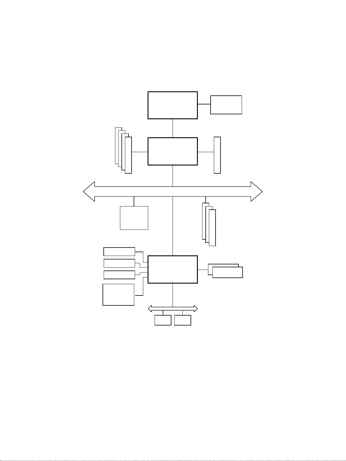
Processor. The functio nal compo nents o f the UP1 500 are shown in b lock di agram
form in Figure 1-1. A detailed description of system components is provided in
the UP1500 Technical Reference Manual.
UP1500 800-A1 1-2
UP1500 User’s Manual Chapter 1 UP1500 Introduction
Note: Refer to the list of Acronyms on page x of the Preface for an explanation
of terminology used in the block diagram.
DDR
SDRAM
DIMMs
Intel 21143
Controller
KBD/Mouse
USB
Sound
LAN
Alpha 21264B
Alpha Processor
AMD761
System Controller
PCI BUS
ALI M1535D+
PCI-ISA Bridge
DDR
L2 cache
4M or 8M
4X AGP
32Bit, 33MHz
PCI Slots
IDE Ports
FDD
2 Serial Ports
1 Parallel Port
RTC
X bus
BIOS
Figure 1-1 UP1500 Functional Block Diagram
UP1500 800-A1 1-3

UP1500 User’s Manual Chapter 2 System Configuration
Chapter 2 System Configuration
This chapter describes the layout and configuration of the UP1500. It includes
information about switch settings used to determine the UP1500 configuration.
2.1 Board Layout and Components
On-board connectors are provided for the following:
!
AGP and PCI cards
!
IDE and FDD devices
!
USB devices
!
Memory DIMMs
!
Serial and parallel peripherals
!
LAN (Ethernet) port
!
Audio In/Out and Mic In connections
!
Power
These connectors and the configuration switchpack are shown in Figure 2-1,
which depicts the UP1500 and its components. Table 2-1 specifies the
components as indicated in Figure 2-1.
Refer to Appendix A for a complete description of the connectors and pinouts
used in the UP1500.
UP1500 800-A1 2-1
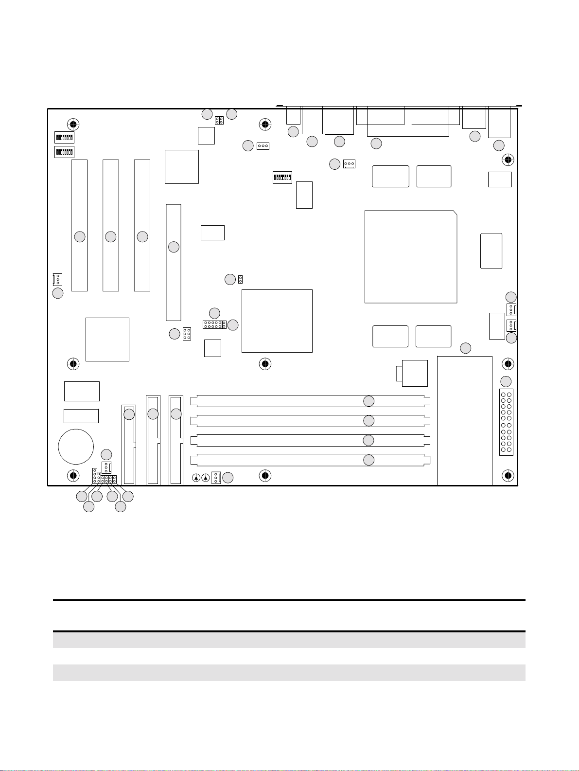
UP1500 User’s Manual Chapter 2 System Configuration
J24
SW2
SW2
SW2SW2
SW3
SW3
SW3SW3
PCI
PCI
PCIPCI
Slot2
Slot2
Slot2Slot2
J8
Flash
Flash
FlashFlash
BIOS
BIOS
BIOSBIOS
RTC
RTC
RTCRTC
PCI
PCI
PCIPCI
Slot1
Slot1
Slot1Slot1
J9 J10
South
South
SouthSouth
Bridge
Bridge
BridgeBridge
ALI
ALI
ALIALI
M1535D+
M1535D+
M1535D+ M1535D+
FDD
FDD
FDDFDD
J17
PCI
PCI
PCIPCI
Slot0
Slot0
Slot0Slot0
IDE0
IDE0IDE0
Network
Network
NetworkNetwork
Controller
Controller
ControllerController
AGP
AGP
AGPAGP
Slot
Slot
SlotSlot
J3
J34
IDE1
IDE1IDE0
IDE1IDE1
J15 J16
Intel
Intel
IntelIntel
21143
21143
2114321143
J38 J39
LAN
LAN
LAN LAN
TX
TX
TXTX
FET
FET
FETFET
J35
Reset
Reset
ResetReset
USB
USB
MIC
MIC
MICMIC
AUDIO
AUDIO
AUDIOAUDIO
J12
J14
SW1
SW1
SW1SW1
FET
FET
FETFET
J1
North
North
NorthNorth
Bridge
Bridge
J2
BridgeBridge
AMD 761
AMD 761
AMD 761AMD 761
DIMM 0
DIMM 0
DIMM 0DIMM 0
DIMM 1
DIMM 1
DIMM 1DIMM 1
LAN
LAN
LANLAN
Conn.
Conn.
Conn.Conn.
J11J13
J37
Serial/Par all e l Co nn .
Serial/Par all e l Co nn .
Serial/Par all e l Co nn .Serial/Par all e l Co nn .
J18
CACHE
CACHE
CACHECACH E
SRAM
SRAM
SRAMSRAM
CACHE
CACHE
CACHECACH E
SRAM
SRAM
SRAMSRAM
J4
J5
CPU
CPU
CPUCPU
21264B
21264B
21264B21264B
FET
FET
FETFET
CACHE
CACHE
CACHECACH E
SRAM
SRAM
SRAMSRAM
CACHE
CACHE
CACHECACH E
SRAM
SRAM
SRAMSRAM
USBUSB
Conn.
Conn.
Conn.Conn.
J19
P1
VRM for CPU
VRM for CPU
VRM for CPUVRM for CPU
Mouse
Mouse
MouseMouse
Conn.
Conn.
Conn.Conn.
TAG
TAG
TAGTAG
SRAM
SRAM
SRAMSRAM
KBD/
KBD/
KBD/KBD/
J20
FET
FET
FETFET
FET
FET
FETFET
J32
J33
J21
BATTERY
BATTERY
BATTERYBATTERY
J26 J25 J29 J27
J28 J30
J31
J36
DIMM 2DIMM 2
DIMM 3
DIMM 3
DIMM 3DIMM 3
J6
J7
DIMM 2
DIMM 2
Figure 2-1 UP1500 Layout
Table 2-1
Comp.
No.
UP1500
Connector Component List
Specification
Comp.
No.
Specification
J1 PLL Bypass Mode Selector J2 PLL Test Mode Selector
J3 AGP Connector J4 184-pin DDR DIMM Socket, Slot 0
J5 184-pin DDR DIMM Socket, Slot 1 J6 184-pin DDR DIMM Socket, Slot 2
J7 184-pin DDR DIMM Socket, Slot 3 J8 32-bit PCI Connector, Slot 2
UP1500 800-A1 2-2

UP1500 User’s Manual Chapter 2 System Configuration
Table 2-1
Comp.
No.
J9 32-bit PCI Connector, Slot 1 J10 32-bit PCI Connector, Slot 0
J11
J13 Audio In/Out Connector J14 Compact Disk (CD) Audio In Connector
J15 Primary IDE Connector J16 Secondary IDE Connector
J17 Floppy Disk Drive (FDD) Connector J18 Serial/Parallel I/O Port
J19 USB Port J20 Keyboard/Mouse Port
J21 ATX Power Connector J22 Not Used
J23 Not Used J24
J25 Power Button Connector J26 Speaker Cable Connector
J27
J29 Reset Button Connector J30 Keybord Lock Cable Connector
J31 System Fan Connector 0 J32 CPU Fan Connector 0
J33 CPU Fan Connector 1 J34 Debug Port
UP1500
Local Area Network (LAN RJ-45
Ethernet) Connector
Hard Disk Drive (HDD) Activity LED
Connector
Connector Component List (Continued)
Specification
Comp.
No.
J12 Mic In Connector
System Management (SM) Bus Extender
Port
J28 Power LED Connector
Specification
J35
J37 System Controller Fan Connector J38 Network Receive LED Connector
39 Network Active LED Connector
Electrically Programmable Logic Device
(EPLD) Program Port
J36 System Fan Connector 1
2.2 Memory Subsystem
2.2.1 Memory Configuration
The memory subsystem has two DIMM bank with four independent slots. (See
Figure 2-2) Each slot accepts 184-pin, PC133 DDR SDRAM Registered SPD
DIMM modules.
UP1500 800-A1 2-3
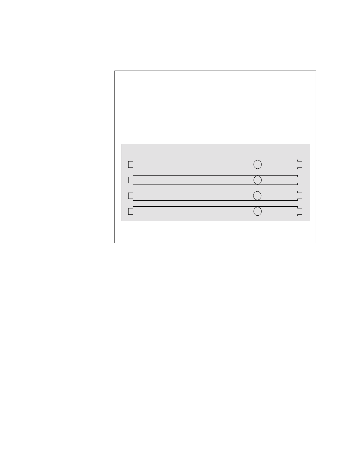
UP1500 User’s Manual Chapter 2 System Configuration
The following DIMM sizes may be used :
128 MB
256 MB
512 MB
1 GB
Memory Subsystem
Memory Subsystem
Memory SubsystemMemory Subsystem
Figure 2-2 Memory Subsystem
2.2.2 Memory Guidelines
Use the following rules to populate the UP1500 memory subsystem :
!
Populate S lot 1 (J3) first.
!
DIMM size can be 128 MB, 256 MB, 512 MB, or 1GB.
!
Each slot can use different sized DIMMs.
!
Memory is supported in a size range between 128 MB (minimum) to 4 GB
(maximum)
DIMM Slot 0
DIMM Slot 0
DIMM Slot 0DIMM Slot 0
DIMM Slot 1
DIMM Slot 1
DIMM Slot 1DIMM Slot 1
DIMM Slot 2
DIMM Slot 2
DIMM Slot 2DIMM Slot 2
DIMM Slot 3
DIMM Slot 3
DIMM Slot 3DIMM Slot 3
J4
J5
J6
J7
See Table 2-2 for typical memory configurations.
Note: For a list of supported memory manufacture’s and parts, check Samsung
Electroni cs Co.,Ltd. webs ite for the UP1500 Har d war e Compati bility L ist
(HCL) :
http://www.alpha.samsung.com/
UP1500 800-A1 2-4

UP1500 User’s Manual Chapter 2 System Configuration
.
Table 2-2 Typical UP1500 Memory Configurations
1 DIMM
Devices used on DIMM
64 Mbit (4M x 4 x 4 banks) 256 Mbytes 512 Mbytes 768 Mbytes 1 Gbytes
64 Mbit (2M x 8 x 4 banks) 128 Mbytes 256 Mbytes 384 Mbytes 512 Mbytes
128 Mbit (8M x 4 x 4 banks) 512 Mbytes 1 Gbytes 1.5 Gbytes 2 Gbytes
128 Mbit (4M x 8 x 4 banks) 256 Mbytes 512 Mbytes 768 Mbytes 1 Gbytes
128 Mbit (2M x 16 x 4 banks) 128 Mbytes 256 Mbytes 384 Mbytes 512 Mbytes
256 Mbit (16M x 4 x 4 banks) 1 Gbytes 2 Gbytes 3 Gbytes 4 Gbytes
256 Mbit (8M x 8 x 4 banks) 512 Mbytes 1 Gbytes 1.5 Gbytes 2 Gbytes
256 Mbit (4M x 16 x 4 banks) 256 Mbytes 512 Mbytes 768 Mbytes 1 Gbytes
512 Mbit (16M x 4 x 4 banks) 1 Gbytes 2 Gbytes 3 Gbytes 4 Gbytes
512 Mbit (8M x 16 x 4 banks) 512 Mbytes 1 Gbytes 1.5 Gbytes 2 Gbytes
Note: The maximum address space supported by the AMD-761 system control-
(2 rows)
x64/x72
ler is 4 Gbytes
2 DIMMs
(2 rows each)
x64/x72
2 DIMMs
(2 rows each)
x64/x72
4 DIMMs
(2 rows each)
x64/x72
2.3 Configuration Settings
The UP1500 has one configuration switchpack, SW1, which has selectable
settings. These switch settings are organized as follows:
!
Switches 1 and 2—Firmware image selection
!
Switches 4, 5 and 6—System bus speed selection
!
Switches 7 and 8—L2 cache size selection
The location of SW1 is shown in Figure 2-1, in the upper-center of the board.
2.3.1 Firmware Image Selection
Configuration of alternat e fi rmwar e is manage d thr ough setting of switches 1 and
2 on SW1, as shown in Table 2-3. Switches 1 and 2 are On by default, which
boots the UP1500 under SRM Console.
UP1500 800-A1 2-5

UP1500 User’s Manual Chapter 2 System Configuration
Table 2-3 Firmware Configuration Settings (SW1, Switches 1 and
2)
Function Switch 1 Position Switch 2 Position
SRM Console (default) On On
Fail Safe Booter (FSB) Off Off
2.3.2 System Bus Speed Selection
System bus speed is configured using Switches 4, 5 and 6 of SW1, as shown in
Table 2-4.
Table 2-4 System Bus Speed Configuration Settings (SW1, Switches
4, 5 and 6)
Function
100 MHz Off Off Off
133 MHz (default) Off Off On
2.3.3 Cache Size Selection
Cache size is configured using Switches 7 and 8 of SW1, as shown in Table 2-5.
Table 2-5 Cache Size Configuration Settings (SW1, Switches 7 and
8)
Function Switch 7 Position Switch 8 Position
Cache Disable On On
2MB On Off
4 MB Off On
8MB Off Off
Switch 4
Position
Switch 5
Position
Switch 6
Position
UP1500 800-A1 2-6

UP1500 User’s Manual Chapter 2 System Configuration
2.4 Initialization Strapping
The UP1500 has another two switchpacks - SW2, SW3 - which describe the
strapping of the AMD-761 System Controller.
2.4.1 System Clock Speed
System clock speed is encoded using Switches 1 and 2 of SW2.
2.4.2 Disable Divider
Special clock test mode that accomodates a large skew between the 1X and 2X
clocks is enabled using Switch 3 of SW2.
2.4.3 Inclk Delay Enable
Inclock delay of the AMD-761 System Controller is enabled using Switch 4 of
SW2.
2.4.4 CPU Clk Hist
Amount of hysteresis applied to the SysDataOutClk[3:0] and SysAddOutClk
inputs for noise immunity is encoded using Switches 5 and 6 of SW2.
2.4.5 AGP Clk MUX
Input to APLL clock mux for PLL test mode is sel ected using Swit ches 7 and 8 of
SW2 and Switch 1 of SW3.
UP1500 800-A1 2-7
 Loading...