

Page 1

LCD-TV
Chassis : N73A
Model : UN32B6000VFXZA
Manual
SERVICE
TFT-LCD TV Contents
1. Precautions
2. Product specications
Disassembly and
3.
4. Troubleshooting
Exploded View & Part List
5.
Wiring Diagram
6.
Reassembly
UN32B6000VFXZA
Refer to the service manual in the GSPN (see the rear cover) for the more information.
Page 2

Contents
1. Precautions .............................................................................................................. 1-1
1-1. Safety Precautions ......................................................................................................... 1-1
1-2. Servicing Precautions .....................................................................................................1-2
1-3. Electrostatically Sensitive Devices (ESD) Precautions .................................................. 1-2
1-4. Installation Precautions .................................................................................................. 1-3
2. Product specications ............................................................................................ 2-1
2-1. Feature & Specications ................................................................................................. 2-1
2-2. MJC : Motion Judder Cancellation (FRC)
2-3. InfoLink
2-4. Media Play ...................................................................................................................... 2-8
2-5. Spec Comparison to the Old Models ............................................................................ 2-10
2-6. Accessories .................................................................................................................. 2-11
........................................................................................................................... 2-7
3. Disassembly and Reassembly ............................................................................... 3-1
3-1. Disassembly and Reassembly ....................................................................................... 3-1
4. Troubleshooting ...................................................................................................... 4-1
4-1. Troubleshooting .............................................................................................................. 4-1
4-2. Alignments and Adjustments ........................................................................................ 4-25
4-3. Factory Mode Adjustments ........................................................................................... 4-26
4-4. White Balance - Calibration .......................................................................................... 4-36
4-5. Servicing Information .................................................................................................... 4-38
....................................................................... 2-6
5. Exploded View & Part List ...................................................................................... 5-1
5-1. UN32B6000VF Exploded View ....................................................................................... 5-1
5-4. UN32B6000VF Parts List ............................................................................................... 5-7
6. Wiring Diagram ........................................................................................................ 6-1
6-1. Wiring Diagram 32” ......................................................................................................... 6-1
6-3. Connector Functions ...................................................................................................... 6-5
6-4. Cables ............................................................................................................................ 6-5
Page 3

GSPN (Global Service Partner Network)
Area Web Site
North America http://service.samsungportal.com
Latin America http://latin.samsungportal.com
CIS http://cis.samsungportal.com
Europe http://europe.samsungportal.com
China http://china.samsungportal.com
Asia http://asia.samsungportal.com
Mideast
& Africa http://mea.samsungportal.com
Service Manual is a property of Samsung Electronics Co.,Ltd.
This
Any unauthorized use of Manual can be punished under applicable
International and/or domestic law.
© 2009 Samsung Electronics Co.,Ltd.
All rights reserved.
Printed in Korea
P/N: BN82-00556A-00
Page 4
3. Disassembly and Reassemble
3. Disassembly and Reassembly
This section of the service manual describes the disassembly and reassembly procedures for the UN40B6000VF LCD TV.
WARNING: This monitor contains electrostatically sensitive devices. Use caution when handling these components.
3-1. Disassembly and Reassembly
Cautions: 1. Disconnect the monitor from the power source before disassembly.
2. Follow these directions carefully; never use metal instruments to pry apart the cabinet.
Description Picture Description Screws
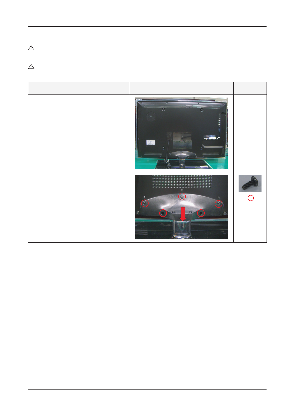
1. Place monitor face down on cushioned table.
Remove screws from the Stand.
Remove stand.
3-1
Page 5

3. Disassembly and Reassemble
Description Picture Description Screws
2. Remove the screws of rear-cover. 40”
46”/55”
2-1. Pull out a AC Power Cord
3. Lift up the rear-cover.
3-2
Page 6

3. Disassembly and Reassemble
Description Picture Description Screws
4. Remove the cables and screws from
SMPS, Main board and Woofer and
Bracket stand link.
40”
46” / 55”
Woofer x 2
3-3
Page 7

3. Disassembly and Reassemble
Description Picture Description Screws
5. Remove the panel bracket screws from the
panel.
3-4
Reassembly procedures are in the reverse order of disassembly procedures.※
Page 8

5. Exploded View & Part List
T0003
M0215
M0014
M0115
M0013
M0027
M0523
5-1. UN32B6000VF Exploded View
5. Exploded View & Part List
5-1
Page 9

5. Exploded View & Part List
5-1-1. UN32B6000VF Parts List
Location No. Code No. Description & Specication Q’ty S.A/S.N.A Remark
T0003 BN96-11248E ASSY COVER P-FRONT;LB6000 32,PC(CLR)+PC( 1 S.A
M0215 BN07-00737A LCD-PANEL;T320FBE1-DB 1 S.A
M0014 BN94-02657T ASSY PCB MAIN;UN32B6000VFXZA 1 S.A
M0115 BN61-05486B BRACKET-STAND LINK;UB6000 32inch,SECC,T2 1 S.N.A
M0523 BN96-10779A ASSY STAND P-GUIDE;NECK;LB700,40,PC,CLEA 1 S.N.A
M0013 BN96-11254E ASSY COVER P-REAR;B7000 32,PCM T0.5,BKN- 1 S.A
M0027 BN96-12372A ASSY STAND P-BASE;32,LB650,TEMPERED GLAS 1 S.A
5-2
Page 10

5. Exploded View & Part List
5-5. UN32B6000VF Parts List
Level Location No. Code No. Description & Specication Q’ty SA/SNA Remark
UN32B6000VFXZA UN32B6000VF,N73A/32BV1-G6V,32,LCD-TV,UNI
0.1 M0001 BN90-02075E ASSY COVER FRONT;32 B6000 1 S.N.A
..2 T0003 BN96-11248E ASSY COVER P-FRONT;LB6000 32,PC(CLR)+PC( 1 S.A
...3 T0069 AA60-00091K SPACER-FELT;FELT,330X10,BLK,T0.35 4 S.N.A
...3 BN61-04661A BRACKET-STOPPER;L650,SK-5,T0.4,Plating,H 2 S.N.A
...3 BN63-01925A FELT-VIBRATION;42D5,FELT,T0.35,10,370 2 S.N.A
...3 CCM1 BN63-02183F COVER-SHEET;Rhcm,PE Vinyl,T0.05,900mm,20 0.74 S.N.A
...3 CCM1 BN63-05199B COVER-SHEET;AMBER,PE,T0.08,W65mm,200M,CL 2.4 S.N.A
...3 CCM1 BN63-05199G COVER-SHEET;AMBER,PE,T0.08,W115mm,200M,C 1 S.N.A
...3 M0112 BN63-05763C COVER-FRONT;UB6000 32,PC(CLR)+PC(Rose Bl 1 S.N.A
...3 T0175 BN96-09470F ASSY SPEAKER P;8ohm,4pin,15W,R:650 / L:4 1 S.A
...3 BN96-11260A ASSY HOLDER P-BOSS;LB7000 32,ABS V0,BLK 1 S.N.A
....4 T0069 AA60-00091E SPACER-FELT;FELT,100X10,BLK,T0.5 1 S.N.A
....4 BN61-03261Z BOSS-TAPE;T1.1,W16,DARK GRAY 3M #4711,VH 0.35 S.N.A
....4 BN61-04692A BOSS-PRIMER;#94,clear,35cps 0.001 S.N.A
....4 BN61-05484A HOLDER-BOSS BOTTOM;UB6000 32inch,ABS,Bla 1 S.N.A
....4 BN61-05728A BOSS-TAPE;UB7000,T0.4,W10,DARK GRAY 0.288 S.N.A
...3 T0382 BP61-00509C HOLDER-CARE;PJT,ACRYL-FOAM,T0.25,W20.0mm 0.16 S.N.A
...3 BN96-10736L ASSY BOARD P-TOUCH FUNCTION&PO;UN32B6000 1 S.A
....4 M2893 BN39-01180B LEAD CONNECTOR;UE40B7000WWXXC,UL2835#30, 1 S.A
....4 M2893 BN39-01181D LEAD CONNECTOR;UN32B6000VF,UL1061#28,6/5 1 S.A
....4 M0102 BN96-10733A ASSY BLU P;UE40B7000WWXXC,MB-M0809-WHITE 1 S.N.A
....4 BN96-10735A ASSY BOARD P-TOUCH POWER&IR;LN46B7000WFX 1 S.N.A
....4 M0175 BN96-10736A ASSY BOARD P-TOUCH FUNCTION;LN46B7000WFX 1 S.N.A
...3 BN64-01021B DECORATION-BOTTOM;UB6000,PC,clear,Hot st 1 S.N.A
0.1 M0002 BN90-02108E ASSY COVER REAR;32 B6000 1 S.N.A
..2 T0081 6001-000799 SCREW-MACHINE;BH,+,M3,L5,ZPC(BLK),SWRCH1 3 S.N.A
..2 C/REAR+PAN 6003-000133 SCREW-TAPTYPE;BH,+,-,S,M4,L8,ZPC(BLK),SW 2 S.N.A
..2 H/CORD+PAN 6003-000337 SCREW-TAPTYPE;BH,+,S,M4,L10,ZPC(BLK),SWR 1 S.N.A
..2 C/FRONT+C/ 6003-001003 SCREW-TAPTYPE;BH,+,B,M4,L12,ZPC(BLK),SWR 12 S.N.A
..2 C/REAR+PAN 6011-001815 BOLT-ETC;M8,L12,ZPC(Black),SWRCH18A,WSP, 4 S.N.A
..2 BN61-04922C HOLDER-CORD;LB7000 46,PC+ABS,V0,BLK 1 S.N.A
..2 M0013 BN96-11254E ASSY COVER P-REAR;B7000 32,PCM T0.5,BKN- 1 S.A
...3 AA60-00091A SPACER;FELT,150X10,BLK,T0.35 1 S.N.A
...3 T0069 AA60-00091H SPACER-FELT;FELT,150X10,BLK,T1.0 2 S.N.A
...3 M0279 BN63-00870A FELT;AS17UO,FELT,0.3,10,287 1 S.N.A
...3 M0006 BN63-05764A COVER-REAR;UB6000 32inch,PCM,T0.5,BKN-P8 1 S.A
...3 BN96-10996E ASSY MISC P-INSULATOR;LED TV,UB6000/7000 1 S.N.A
....4 T0278 BN60-00122A SPACER-SPONGE;UB7000,CR,L265,T2.0,W10 2 S.N.A
0.1 M0216 BN90-02223A ASSY STAND;50 INSIGNIA 1 S.N.A
..2 M0523 BN96-11440B ASSY STAND P-GUIDE;UB6000 32,PC+G/F,20%, 1 S.A
...3 T0524 6902-001048 BAG PE;LDPE,T0.05,W160,L300,TRP,4g 1 S.N.A
...3 T0920 BN61-05485A GUIDE-STAND;UB6000 32,PET+PC G/F(15%) V2 1 S.N.A
...3 BN68-02215D MANUAL FLYER-STAND GUIDE;comm,samsung,W/ 1 S.N.A
...3 BN96-12031A ASSY ACCESSORY-SCREW;09 LEDTV(40/46),ALL 1 S.N.A
....4 G/STAND+G/ 6003-001003 SCREW-TAPTYPE;BH,+,B,M4,L12,ZPC(BLK),SWR 4 S.N.A
5-9
Page 11

5. Exploded View & Part List
Level Location No. Code No. Description & Specication Q’ty SA/SNA Remark
....4 6902-000336 BAG ZIPPER;LDPE,T0.05,W70,L80,TRP,0.500g 1 S.N.A
....4 BN68-02215G MANUAL FLYER-STAND GUIDE;B6000 ~ 8000,SA 1 S.N.A
...3 BN96-12031C ASSY ACCESSORY-SCREW;09 LEDTV,6003-00013 1 S.N.A
....4 STAND+SET 6003-000133 SCREW-TAPTYPE;BH,+,-,S,M4,L8,ZPC(BLK),SW 5 S.N.A
....4 6902-000336 BAG ZIPPER;LDPE,T0.05,W70,L80,TRP,0.500g 1 S.N.A
....4 BN68-02215H MANUAL FLYER-STAND GUIDE;B6000 ~ 8000,SA 1 S.N.A
..2 M0027 BN96-12372A ASSY STAND P-BASE;32,LB650,TEMPERED GLAS 1 S.A
...3 B/S/STAND+ 6003-001003 SCREW-TAPTYPE;BH,+,B,M4,L12,ZPC(BLK),SWR 3 S.N.A
...3 BN61-04692A BOSS-PRIMER;#94,clear,35cps 0.1 S.N.A
...3 BN61-04731B BOSS-TAPE;AMBER,ACRYL,T1.1,W12.0mm,WHITE 0.29 S.N.A
...3 BN61-04855A BRACKET-SWIVEL BOTTOM;B650 40,SECC,T2.0 1 S.N.A
...3 BN61-05254A HOLDER-SWIVEL RING BOTTOM;LB700 40,POM H 1 S.N.A
...3 BN61-05653A BRACKET-STAND BOTTOM;B650 32,SECC,T2.0 1 S.N.A
...3 BN61-05826A BOSS-BOND;#760,Poly urethane,Black 1.2 S.N.A
...3 CCM1 BN63-04755F COVER-SHEET;PE,T0.05,W410mm,200M,600FE,C 0.61 S.N.A
...3 BN63-05530B COVER-STAND GLASS;32,LB650,GLASS,T8.0,RO 1 S.N.A
...3 T0056 BN63-05537A COVER-DECORATION;UB7000 40inch,ABS,PMMA, 1 S.N.A
...3 BN68-01402J MANUAL FLYER-STAND GUIDE;COMM,SAMSUNG,En 1 S.N.A
...3 M0126 BN73-00215A RUBBER-FOOT;40LB650,RUBBER,15*25,60,4.0, 2 S.N.A
...3 M0126 BN73-00217A RUBBER-FOOT;LB650,RUBBER,DIA30,7.5,Dark 4 S.N.A
...3 BN74-00031A GREASE;kanto-kasei FL-955,grease,wht 0.4 S.N.A
...3 M0523 BN96-10779A ASSY STAND P-GUIDE;NECK;LB700,40,PC,CLEA 1 S.A
....4 BN61-05248A GUIDE-STAND NECK;LB650,32,PC,CLEAR(TP27) 1 S.N.A
....4 BN61-05271A HOLDER-INSERT;40 LB750,PC,EXTRUSION,CLEA 1 S.N.A
...3 BN61-05238A HOLDER-SWIVEL RING TOP;LB700 40,POM HB,A 1 S.N.A
0.1 M0017 BN91-03716M ASSY CHASSIS;UN32B6000VFXZA 1 S.N.A
..2 M0014 BN94-02657T ASSY PCB MAIN;UN32B6000VFXZA 1 S.A
...3 SUB01 0202-001557 SOLDER-CREAM;LST57-A,D38-63,42SN/57BI/1A 5.42 S.N.A
...3 T0245 0202-001608 SOLDER-WIRE FLUX;LFC7-107,D0.8,99.3Sn/0. 0.25 S.N.A
...3 CN1204 3701-001571 CONNECTOR-DSUB;15P,3ROW,FEMALE,ANGLE,TIN 1 S.A
...3 CN906 3707-001090 CONNECTOR-OPTICAL;angle(ULTRA SLIM),SPDI 1 S.A
...3 CN330 3711-003847 HEADER-BOARD TO CABLE;BOX,12P,1R,2mm,ANG 1 S.A
...3 CN201 3711-005884 HEADER-BOARD TO BOARD;BOX,30P,2R,2mm,ANG 1 S.A
...3 CN330 3711-006715 HEADER-BOARD TO CABLE;BOX,4P,1R,2.5mm,AN 1 S.N.A
...3 CN903 3722-001051 JACK-USB;4P/1C,AU,BLK,ANGLE,A TYPE 1 S.A
...3 CN904 3722-001051 JACK-USB;4P/1C,AU,BLK,ANGLE,A TYPE 1 S.A
...3 JA330 3722-002846 JACK-PHONE;1/6,NI,BLACK,ANGLE 1 S.A
...3 JA330 3722-002846 JACK-PHONE;1/6,NI,BLACK,ANGLE 1 S.A
...3 JA330 3722-002846 JACK-PHONE;1/6,NI,BLACK,ANGLE 1 S.A
...3 JA333 3722-002847 JACK-PIN;5P(ULTRA SLIM),NI,BLACK,ANGLE(S 1 S.A
...3 CN1101 3722-002849 JACK-MODULAR;8P/8C(ULTRA SLIM),YES,ANGLE 1 S.A
...3 T0562 6046-001015 STAND OFF;#4-40,L5,Ni PLT,C3601,M3 2 S.N.A
...3 CIS3 BN40-00139A TUNER;DTVS20FFH102A,DTVS20FFH102A,VSB(NT 1 S.A
...3 BRACKET_AV BN61-04923A BRACKET-AV;LB700 40,PCM,T0.5,BKN-P824, N 1 S.N.A
...3 T0066 BN62-00042A HEAT SINK-ES;30*30*5,Ceramic,T1.5,TAPE 1 S.A
...3 T0066 BN62-00043A HEAT SINK-ES;40*40*5,Ceramic,T1.5,TAPE 1 S.A
...3 T0174 BN97-03201Q ASSY SMD;UN32B6000VFXZA 1 S.N.A
....4 SUB05 0202-001477 SOLDER-CREAM;LST309-M,D20~45um,96.5Sn/3A 2.361 S.N.A
....4 D1228 0401-001049 DIODE-SWITCHING;LS4148,75V,150mA,SOD-80, 1 S.A
....4 D1229 0401-001049 DIODE-SWITCHING;LS4148,75V,150mA,SOD-80, 1 S.A
5-10
Page 12

5. Exploded View & Part List
Level Location No. Code No. Description & Specication Q’ty SA/SNA Remark
....4 D1230 0401-001049 DIODE-SWITCHING;LS4148,75V,150mA,SOD-80, 1 S.A
....4 D1231 0401-001049 DIODE-SWITCHING;LS4148,75V,150mA,SOD-80, 1 S.A
....4 D1501D 0401-001049 DIODE-SWITCHING;LS4148,75V,150mA,SOD-80, 1 S.A
....4 D1502 0401-001049 DIODE-SWITCHING;LS4148,75V,150mA,SOD-80, 1 S.A
....4 D1503 0401-001049 DIODE-SWITCHING;LS4148,75V,150mA,SOD-80, 1 S.A
....4 D1504 0401-001049 DIODE-SWITCHING;LS4148,75V,150mA,SOD-80, 1 S.A
....4 D1603 0401-001049 DIODE-SWITCHING;LS4148,75V,150mA,SOD-80, 1 S.A
....4 D1604 0401-001049 DIODE-SWITCHING;LS4148,75V,150mA,SOD-80, 1 S.A
....4 D1622 0401-001049 DIODE-SWITCHING;LS4148,75V,150mA,SOD-80, 1 S.A
....4 D1101 0401-001056 DIODE-SWITCHING;MMBD4148SE,100V,200mA,SO 1 S.A
....4 D1102 0401-001056 DIODE-SWITCHING;MMBD4148SE,100V,200mA,SO 1 S.A
....4 D1103 0401-001056 DIODE-SWITCHING;MMBD4148SE,100V,200mA,SO 1 S.A
....4 D1104 0401-001056 DIODE-SWITCHING;MMBD4148SE,100V,200mA,SO 1 S.A
....4 D1225 0401-001056 DIODE-SWITCHING;MMBD4148SE,100V,200mA,SO 1 S.A
....4 D1226 0401-001056 DIODE-SWITCHING;MMBD4148SE,100V,200mA,SO 1 S.A
....4 D1227 0401-001056 DIODE-SWITCHING;MMBD4148SE,100V,200mA,SO 1 S.A
....4 D1401 0401-001056 DIODE-SWITCHING;MMBD4148SE,100V,200mA,SO 1 S.A
....4 D1402 0401-001056 DIODE-SWITCHING;MMBD4148SE,100V,200mA,SO 1 S.A
....4 D1406 0401-001056 DIODE-SWITCHING;MMBD4148SE,100V,200mA,SO 1 S.A
....4 D1407 0401-001056 DIODE-SWITCHING;MMBD4148SE,100V,200mA,SO 1 S.A
....4 D1417 0401-001056 DIODE-SWITCHING;MMBD4148SE,100V,200mA,SO 1 S.A
....4 D1418 0401-001056 DIODE-SWITCHING;MMBD4148SE,100V,200mA,SO 1 S.A
....4 D1419 0401-001056 DIODE-SWITCHING;MMBD4148SE,100V,200mA,SO 1 S.A
....4 D1420 0401-001056 DIODE-SWITCHING;MMBD4148SE,100V,200mA,SO 1 S.A
....4 D1601 0401-001056 DIODE-SWITCHING;MMBD4148SE,100V,200mA,SO 1 S.A
....4 D1609 0401-001056 DIODE-SWITCHING;MMBD4148SE,100V,200mA,SO 1 S.A
....4 D1430 0401-001099 DIODE-SWITCHING;1N4148WS,75V,150mA,SOD-3 1 S.N.A
....4 D0254 0402-001207 DIODE-SCHOTTKY;UPS5819,40V,1000mA,DO-216 1 S.A
....4 D1602 0403-000002 DIODE-ZENER;VLZ5V6B,5.45/5.73V,500mW,SOD 1 S.A
....4 D1216 0403-001180 DIODE-ZENER;BZX84C6V2,5.8-6.6V,350mW,SOT 1 S.A
....4 D1217 0403-001180 DIODE-ZENER;BZX84C6V2,5.8-6.6V,350mW,SOT 1 S.A
....4 D1218 0403-001180 DIODE-ZENER;BZX84C6V2,5.8-6.6V,350mW,SOT 1 S.A
....4 D1219 0403-001180 DIODE-ZENER;BZX84C6V2,5.8-6.6V,350mW,SOT 1 S.A
....4 D1220 0403-001180 DIODE-ZENER;BZX84C6V2,5.8-6.6V,350mW,SOT 1 S.A
....4 D1221 0403-001180 DIODE-ZENER;BZX84C6V2,5.8-6.6V,350mW,SOT 1 S.A
....4 D1309 0403-001180 DIODE-ZENER;BZX84C6V2,5.8-6.6V,350mW,SOT 1 S.A
....4 D1310 0403-001180 DIODE-ZENER;BZX84C6V2,5.8-6.6V,350mW,SOT 1 S.A
....4 D1311 0403-001180 DIODE-ZENER;BZX84C6V2,5.8-6.6V,350mW,SOT 1 S.A
....4 D1312 0403-001180 DIODE-ZENER;BZX84C6V2,5.8-6.6V,350mW,SOT 1 S.A
....4 D1313 0403-001180 DIODE-ZENER;BZX84C6V2,5.8-6.6V,350mW,SOT 1 S.A
....4 D1314 0403-001180 DIODE-ZENER;BZX84C6V2,5.8-6.6V,350mW,SOT 1 S.A
....4 D1403 0403-001180 DIODE-ZENER;BZX84C6V2,5.8-6.6V,350mW,SOT 1 S.A
....4 D1405 0403-001180 DIODE-ZENER;BZX84C6V2,5.8-6.6V,350mW,SOT 1 S.A
....4 D1408 0403-001180 DIODE-ZENER;BZX84C6V2,5.8-6.6V,350mW,SOT 1 S.A
....4 D1409 0403-001180 DIODE-ZENER;BZX84C6V2,5.8-6.6V,350mW,SOT 1 S.A
....4 D1410 0403-001180 DIODE-ZENER;BZX84C6V2,5.8-6.6V,350mW,SOT 1 S.A
....4 D1414 0403-001180 DIODE-ZENER;BZX84C6V2,5.8-6.6V,350mW,SOT 1 S.A
....4 D1415 0403-001180 DIODE-ZENER;BZX84C6V2,5.8-6.6V,350mW,SOT 1 S.A
....4 D1416 0403-001180 DIODE-ZENER;BZX84C6V2,5.8-6.6V,350mW,SOT 1 S.A
....4 D0254 0404-001404 DIODE-SCHOTTKY;BAT721C,40V,200mA,SOT-23, 1 S.A
....4 D0254 0404-001404 DIODE-SCHOTTKY;BAT721C,40V,200mA,SOT-23, 1 S.A
5-11
Page 13

5. Exploded View & Part List
Level Location No. Code No. Description & Specication Q’ty SA/SNA Remark
....4 D0254 0404-001404 DIODE-SCHOTTKY;BAT721C,40V,200mA,SOT-23, 1 S.A
....4 D901 0406-001200 DIODE-TVS;RCLAMP0504F,6/-/-V,150W,SC-70 1 S.A
....4 D902 0406-001200 DIODE-TVS;RCLAMP0504F,6/-/-V,150W,SC-70 1 S.A
....4 D1421 0406-001271 DIODE-TVS;RCLAMP0524P,6/-/-V,150W,SLP251 1 S.A
....4 D1422 0406-001271 DIODE-TVS;RCLAMP0524P,6/-/-V,150W,SLP251 1 S.A
....4 D1423 0406-001271 DIODE-TVS;RCLAMP0524P,6/-/-V,150W,SLP251 1 S.A
....4 D1424 0406-001271 DIODE-TVS;RCLAMP0524P,6/-/-V,150W,SLP251 1 S.A
....4 D1425 0406-001271 DIODE-TVS;RCLAMP0524P,6/-/-V,150W,SLP251 1 S.A
....4 D1426 0406-001271 DIODE-TVS;RCLAMP0524P,6/-/-V,150W,SLP251 1 S.A
....4 D1427 0406-001271 DIODE-TVS;RCLAMP0524P,6/-/-V,150W,SLP251 1 S.A
....4 D1428 0406-001271 DIODE-TVS;RCLAMP0524P,6/-/-V,150W,SLP251 1 S.A
....4 D1429 0407-000123 DIODE-SWITCHING;DAN202K,80V,100mA,SOT-23 1 S.N.A
....4 D1606 0407-000123 DIODE-SWITCHING;DAN202K,80V,100mA,SOT-23 1 S.N.A
....4 D801 0407-000123 DIODE-SWITCHING;DAN202K,80V,100mA,SOT-23 1 S.N.A
....4 Q1003L 0501-000445 TR-SMALL SIGNAL;KTC3875S-Y,NPN,150mW,SOT 1 S.A
....4 Q1101 0501-000445 TR-SMALL SIGNAL;KTC3875S-Y,NPN,150mW,SOT 1 S.A
....4 Q1401 0501-000445 TR-SMALL SIGNAL;KTC3875S-Y,NPN,150mW,SOT 1 S.A
....4 Q1402 0501-000445 TR-SMALL SIGNAL;KTC3875S-Y,NPN,150mW,SOT 1 S.A
....4 Q1501 0501-000445 TR-SMALL SIGNAL;KTC3875S-Y,NPN,150mW,SOT 1 S.A
....4 Q1502 0501-000445 TR-SMALL SIGNAL;KTC3875S-Y,NPN,150mW,SOT 1 S.A
....4 Q1504 0501-000445 TR-SMALL SIGNAL;KTC3875S-Y,NPN,150mW,SOT 1 S.A
....4 Q1605 0501-000445 TR-SMALL SIGNAL;KTC3875S-Y,NPN,150mW,SOT 1 S.A
....4 Q1606 0501-000445 TR-SMALL SIGNAL;KTC3875S-Y,NPN,150mW,SOT 1 S.A
....4 Q201L 0501-000445 TR-SMALL SIGNAL;KTC3875S-Y,NPN,150mW,SOT 1 S.A
....4 Q203L 0501-000445 TR-SMALL SIGNAL;KTC3875S-Y,NPN,150mW,SOT 1 S.A
....4 Q1503 0501-000669 TR-SMALL SIGNAL;KTA1505Y,PNP,150mW,SOT-2 1 S.A
....4 Q1505 0501-000669 TR-SMALL SIGNAL;KTA1505Y,PNP,150mW,SOT-2 1 S.A
....4 Q409 0505-001916 FET-SILICON;Si4800BDY,N,30V,9A,0.03ohm,2 1 S.A
....4 IC1302 1001-000164 IC-ANALOG MULTIPLEX;74HC4052,CMOS,SOP,16 1 S.A
....4 IC1103 1001-001109 IC-ANALOG SWITCH;FST3125M,BUS SWITCH & C 1 S.A
....4 IC106 1001-001573 IC-VIDEO SWITCH;SiI9287BCNUTR,QFN,72P,10 1 S.A
....4 IC1301 1006-001266 IC-LINE TRANSCEIVER;3232,TSSOP,16P,174MI 1 S.A
....4 IC112 1103-000129 IC-EEPROM;24C02,2Kbit,256x8,SOP,8P,5x4mm 1 S.A
....4 IC112 1103-000129 IC-EEPROM;24C02,2Kbit,256x8,SOP,8P,5x4mm 1 S.A
....4 IC112 1103-001385 IC-EEPROM;AT24C256,256Kbit,32Kx8,SOP,8P, 1 S.A
....4 IC112 1103-001415 IC-EEPROM;AT93C46D,1Kbit,128x8/64x16,SOP 1 S.N.A
....4 IC701 1105-001931 IC-DDR2 SDRAM;K4T51163Q,DDR2-800,512Mbit 1 S.N.A
....4 IC702 1105-001931 IC-DDR2 SDRAM;K4T51163Q,DDR2-800,512Mbit 1 S.N.A
....4 IC703 1105-001931 IC-DDR2 SDRAM;K4T51163Q,DDR2-800,512Mbit 1 S.N.A
....4 IC704 1105-001931 IC-DDR2 SDRAM;K4T51163Q,DDR2-800,512Mbit 1 S.N.A
....4 T0124 1201-002796 IC-POWER AMP;STA339BWS,PSSO,36P,10.3x7.5 1 S.A
....4 T0124 1201-002796 IC-POWER AMP;STA339BWS,PSSO,36P,10.3x7.5 1 S.A
....4 T0087 1203-001815 IC-POSI.FIXED REG.;78M09,TO-252,3P,PLAST 1 S.A
....4 T0087 1203-001816 IC-POSI.FIXED REG.;78M08,TO-252,3P,-,PLA 1 S.A
....4 T0087 1203-002835 IC-POSI.FIXED REG.;KIA7805AF,DPAK,3P,6.6 1 S.A
....4 T0087 1203-002842 IC-POSI.FIXED REG.;AP1117D-33A,TO-252,3P 1 S.A
....4 T0087 1203-002974 IC-POSI.FIXED REG.;AP1117D-25A,TO-252,3P 1 S.A
....4 IC1605 1203-004363 IC-VOL. DETECTOR;RT9818C-29PV,SOT-23,3P, 1 S.A
....4 IC1601 1203-004364 IC-VOL. DETECTOR;RT9818C-42PV,SOT-23,3P, 1 S.A
....4 IC203 1203-004879 IC-DC/DC CONVERTER;MP8668DL,QFN,14P,3x4m 1 S.A
....4 T0087 1203-005134 IC-POSI.FIXED REG.;RT9167A-33PB,SOT-23-5 1 S.A
5-12
Page 14

5. Exploded View & Part List
Level Location No. Code No. Description & Specication Q’ty SA/SNA Remark
....4 IC207 1203-005538 IC-DC/DC CONVERTER;AOZ1021HAIL,SOP,8P,4. 1 S.A
....4 IC504 1203-005559 IC-BACKLIGHT DRIVER;MP3302DJ,TSOT23,5P,2 1 S.A
....4 T0087 1203-005713 IC-POSI.FIXED REG.;S-1172B33-E6T1G,HSOP, 1 S.A
....4 T0087 1203-005713 IC-POSI.FIXED REG.;S-1172B33-E6T1G,HSOP, 1 S.A
....4 IC118 1204-003010 IC-VIDEO PROCESS;SDP84,PBGA,324P,23x23mm 1 S.A
....4 IC601 1204-003011 IC-DECODER;SDP83,PBGA,729P,34x34mm,PLAST 1 S.A
....4 IC1102 1205-002941 IC-ETHERNET CONTROLLER;RTL8100CSL-LF,LQF 1 S.N.A
....4 IC1604 1205-003201 IC-BUS SWITCH;TC7WB125FK,SSOP,8P,2x2.3mm 1 S.A
....4 IC1501 1205-003352 IC-CODEC;WM8593SEFT/V,TQFP,64P,10x10mm,P 1 S.A
....4 IC903 1205-003733 IC-SWITCH;AP2191MPG-13,MSOP-8L-EP,8P,2.9 1 S.A
....4 IC902 1205-003735 IC-SWITCH;AP2151WG-7,SOT25,5P,2.9x1.6mm, 1 S.A
....4 IC503 1209-001830 IC-PLL;IDT6V10012PGG,TSSOP,20P,6.5x4.4mm 1 S.A
....4 D1619 1405-001185 VARISTOR;24Vdc,1.6x0.8x0.36mm,TP 1 S.A
....4 D1105 1405-001233 VARISTOR;30Vdc,5A,1.6x0.8x0.8mm,TP 1 S.A
....4 D1106 1405-001233 VARISTOR;30Vdc,5A,1.6x0.8x0.8mm,TP 1 S.A
....4 D1222 1405-001233 VARISTOR;30Vdc,5A,1.6x0.8x0.8mm,TP 1 S.A
....4 D1223 1405-001233 VARISTOR;30Vdc,5A,1.6x0.8x0.8mm,TP 1 S.A
....4 D1315 1405-001233 VARISTOR;30Vdc,5A,1.6x0.8x0.8mm,TP 1 S.A
....4 D1316 1405-001233 VARISTOR;30Vdc,5A,1.6x0.8x0.8mm,TP 1 S.A
....4 D1317 1405-001233 VARISTOR;30Vdc,5A,1.6x0.8x0.8mm,TP 1 S.A
....4 D1318 1405-001233 VARISTOR;30Vdc,5A,1.6x0.8x0.8mm,TP 1 S.A
....4 D1321 1405-001233 VARISTOR;30Vdc,5A,1.6x0.8x0.8mm,TP 1 S.A
....4 D1322 1405-001233 VARISTOR;30Vdc,5A,1.6x0.8x0.8mm,TP 1 S.A
....4 D1324 1405-001233 VARISTOR;30Vdc,5A,1.6x0.8x0.8mm,TP 1 S.A
....4 D1325 1405-001233 VARISTOR;30Vdc,5A,1.6x0.8x0.8mm,TP 1 S.A
....4 D1611 1405-001233 VARISTOR;30Vdc,5A,1.6x0.8x0.8mm,TP 1 S.A
....4 D1612 1405-001233 VARISTOR;30Vdc,5A,1.6x0.8x0.8mm,TP 1 S.A
....4 D1613 1405-001233 VARISTOR;30Vdc,5A,1.6x0.8x0.8mm,TP 1 S.A
....4 D1614 1405-001233 VARISTOR;30Vdc,5A,1.6x0.8x0.8mm,TP 1 S.A
....4 D1615 1405-001233 VARISTOR;30Vdc,5A,1.6x0.8x0.8mm,TP 1 S.A
....4 D1618 1405-001233 VARISTOR;30Vdc,5A,1.6x0.8x0.8mm,TP 1 S.A
....4 R702 2007-000043 R-CHIP;1Kohm,1%,1/10W,TP,1608 1 S.A
....4 R703 2007-000043 R-CHIP;1Kohm,1%,1/10W,TP,1608 1 S.A
....4 R704 2007-000043 R-CHIP;1Kohm,1%,1/10W,TP,1608 1 S.A
....4 R705 2007-000043 R-CHIP;1Kohm,1%,1/10W,TP,1608 1 S.A
....4 R707 2007-000043 R-CHIP;1Kohm,1%,1/10W,TP,1608 1 S.A
....4 R708 2007-000043 R-CHIP;1Kohm,1%,1/10W,TP,1608 1 S.A
....4 R709 2007-000043 R-CHIP;1Kohm,1%,1/10W,TP,1608 1 S.A
....4 R710 2007-000043 R-CHIP;1Kohm,1%,1/10W,TP,1608 1 S.A
....4 R714 2007-000043 R-CHIP;1Kohm,1%,1/10W,TP,1608 1 S.A
....4 R715 2007-000043 R-CHIP;1Kohm,1%,1/10W,TP,1608 1 S.A
....4 R716 2007-000043 R-CHIP;1Kohm,1%,1/10W,TP,1608 1 S.A
....4 R717 2007-000043 R-CHIP;1Kohm,1%,1/10W,TP,1608 1 S.A
....4 R721 2007-000043 R-CHIP;1Kohm,1%,1/10W,TP,1608 1 S.A
....4 R722 2007-000043 R-CHIP;1Kohm,1%,1/10W,TP,1608 1 S.A
....4 R723 2007-000043 R-CHIP;1Kohm,1%,1/10W,TP,1608 1 S.A
....4 R724 2007-000043 R-CHIP;1Kohm,1%,1/10W,TP,1608 1 S.A
....4 R1509-1 2007-000072 R-CHIP;47ohm,5%,1/10W,TP,1608 1 S.N.A
....4 R1510-1 2007-000072 R-CHIP;47ohm,5%,1/10W,TP,1608 1 S.N.A
....4 R1555 2007-000072 R-CHIP;47ohm,5%,1/10W,TP,1608 1 S.N.A
....4 R1556 2007-000072 R-CHIP;47ohm,5%,1/10W,TP,1608 1 S.N.A
5-13
Page 15

5. Exploded View & Part List
Level Location No. Code No. Description & Specication Q’ty SA/SNA Remark
....4 R1557 2007-000072 R-CHIP;47ohm,5%,1/10W,TP,1608 1 S.N.A
....4 R1558 2007-000072 R-CHIP;47ohm,5%,1/10W,TP,1608 1 S.N.A
....4 R1025 2007-000078 R-CHIP;1Kohm,5%,1/10W,TP,1608 1 S.A
....4 R1026 2007-000078 R-CHIP;1Kohm,5%,1/10W,TP,1608 1 S.A
....4 R1508-1 2007-000090 R-CHIP;10Kohm,5%,1/10W,TP,1608 1 S.A
....4 R423 2007-000109 R-CHIP;1Mohm,5%,1/10W,TP,1608 1 S.N.A
....4 R1678 2007-000124 R-CHIP;2.2Kohm,5%,1/10W,TP,1608 1 S.N.A
....4 R1401 2007-000138 R-CHIP;100ohm,5%,1/16W,TP,1005 1 S.N.A
....4 R1459 2007-000138 R-CHIP;100ohm,5%,1/16W,TP,1005 1 S.N.A
....4 R1460 2007-000138 R-CHIP;100ohm,5%,1/16W,TP,1005 1 S.N.A
....4 R1461 2007-000138 R-CHIP;100ohm,5%,1/16W,TP,1005 1 S.N.A
....4 R1107 2007-000140 R-CHIP;1Kohm,5%,1/16W,TP,1005 1 S.N.A
....4 R1671 2007-000140 R-CHIP;1Kohm,5%,1/16W,TP,1005 1 S.N.A
....4 R231L 2007-000140 R-CHIP;1Kohm,5%,1/16W,TP,1005 1 S.N.A
....4 R316 2007-000140 R-CHIP;1Kohm,5%,1/16W,TP,1005 1 S.N.A
....4 R406 2007-000140 R-CHIP;1Kohm,5%,1/16W,TP,1005 1 S.N.A
....4 R420 2007-000140 R-CHIP;1Kohm,5%,1/16W,TP,1005 1 S.N.A
....4 R824 2007-000140 R-CHIP;1Kohm,5%,1/16W,TP,1005 1 S.N.A
....4 R826 2007-000140 R-CHIP;1Kohm,5%,1/16W,TP,1005 1 S.N.A
....4 R986 2007-000140 R-CHIP;1Kohm,5%,1/16W,TP,1005 1 S.N.A
....4 R1246 2007-000141 R-CHIP;2.2Kohm,5%,1/16W,TP,1005 1 S.N.A
....4 R1247 2007-000141 R-CHIP;2.2Kohm,5%,1/16W,TP,1005 1 S.N.A
....4 R1248 2007-000141 R-CHIP;2.2Kohm,5%,1/16W,TP,1005 1 S.N.A
....4 R1249 2007-000141 R-CHIP;2.2Kohm,5%,1/16W,TP,1005 1 S.N.A
....4 R1504-1 2007-000141 R-CHIP;2.2Kohm,5%,1/16W,TP,1005 1 S.N.A
....4 R1552 2007-000141 R-CHIP;2.2Kohm,5%,1/16W,TP,1005 1 S.N.A
....4 R1563 2007-000141 R-CHIP;2.2Kohm,5%,1/16W,TP,1005 1 S.N.A
....4 R1564 2007-000141 R-CHIP;2.2Kohm,5%,1/16W,TP,1005 1 S.N.A
....4 R1607 2007-000141 R-CHIP;2.2Kohm,5%,1/16W,TP,1005 1 S.N.A
....4 R901 2007-000141 R-CHIP;2.2Kohm,5%,1/16W,TP,1005 1 S.N.A
....4 R903 2007-000141 R-CHIP;2.2Kohm,5%,1/16W,TP,1005 1 S.N.A
....4 R905 2007-000141 R-CHIP;2.2Kohm,5%,1/16W,TP,1005 1 S.N.A
....4 R908 2007-000141 R-CHIP;2.2Kohm,5%,1/16W,TP,1005 1 S.N.A
....4 R911 2007-000141 R-CHIP;2.2Kohm,5%,1/16W,TP,1005 1 S.N.A
....4 R914 2007-000141 R-CHIP;2.2Kohm,5%,1/16W,TP,1005 1 S.N.A
....4 R917 2007-000141 R-CHIP;2.2Kohm,5%,1/16W,TP,1005 1 S.N.A
....4 R920 2007-000141 R-CHIP;2.2Kohm,5%,1/16W,TP,1005 1 S.N.A
....4 R1001 2007-000143 R-CHIP;4.7Kohm,5%,1/16W,TP,1005 1 S.N.A
....4 R1118 2007-000143 R-CHIP;4.7Kohm,5%,1/16W,TP,1005 1 S.N.A
....4 R1130 2007-000143 R-CHIP;4.7Kohm,5%,1/16W,TP,1005 1 S.N.A
....4 R14104 2007-000143 R-CHIP;4.7Kohm,5%,1/16W,TP,1005 1 S.N.A
....4 R14105 2007-000143 R-CHIP;4.7Kohm,5%,1/16W,TP,1005 1 S.N.A
....4 R14106 2007-000143 R-CHIP;4.7Kohm,5%,1/16W,TP,1005 1 S.N.A
....4 R1431 2007-000143 R-CHIP;4.7Kohm,5%,1/16W,TP,1005 1 S.N.A
....4 R1540 2007-000143 R-CHIP;4.7Kohm,5%,1/16W,TP,1005 1 S.N.A
....4 R1569 2007-000143 R-CHIP;4.7Kohm,5%,1/16W,TP,1005 1 S.N.A
....4 R1570 2007-000143 R-CHIP;4.7Kohm,5%,1/16W,TP,1005 1 S.N.A
....4 R1571 2007-000143 R-CHIP;4.7Kohm,5%,1/16W,TP,1005 1 S.N.A
....4 R1606 2007-000143 R-CHIP;4.7Kohm,5%,1/16W,TP,1005 1 S.N.A
....4 R1630 2007-000143 R-CHIP;4.7Kohm,5%,1/16W,TP,1005 1 S.N.A
....4 R1631 2007-000143 R-CHIP;4.7Kohm,5%,1/16W,TP,1005 1 S.N.A
5-14
Page 16

5. Exploded View & Part List
Level Location No. Code No. Description & Specication Q’ty SA/SNA Remark
....4 R1634 2007-000143 R-CHIP;4.7Kohm,5%,1/16W,TP,1005 1 S.N.A
....4 R1635 2007-000143 R-CHIP;4.7Kohm,5%,1/16W,TP,1005 1 S.N.A
....4 R1653 2007-000143 R-CHIP;4.7Kohm,5%,1/16W,TP,1005 1 S.N.A
....4 R1665 2007-000143 R-CHIP;4.7Kohm,5%,1/16W,TP,1005 1 S.N.A
....4 R1667 2007-000143 R-CHIP;4.7Kohm,5%,1/16W,TP,1005 1 S.N.A
....4 R1681 2007-000143 R-CHIP;4.7Kohm,5%,1/16W,TP,1005 1 S.N.A
....4 R204 2007-000143 R-CHIP;4.7Kohm,5%,1/16W,TP,1005 1 S.N.A
....4 R232L 2007-000143 R-CHIP;4.7Kohm,5%,1/16W,TP,1005 1 S.N.A
....4 R302 2007-000143 R-CHIP;4.7Kohm,5%,1/16W,TP,1005 1 S.N.A
....4 R303 2007-000143 R-CHIP;4.7Kohm,5%,1/16W,TP,1005 1 S.N.A
....4 R309 2007-000143 R-CHIP;4.7Kohm,5%,1/16W,TP,1005 1 S.N.A
....4 R536 2007-000143 R-CHIP;4.7Kohm,5%,1/16W,TP,1005 1 S.N.A
....4 R817 2007-000143 R-CHIP;4.7Kohm,5%,1/16W,TP,1005 1 S.N.A
....4 R818 2007-000143 R-CHIP;4.7Kohm,5%,1/16W,TP,1005 1 S.N.A
....4 R821 2007-000143 R-CHIP;4.7Kohm,5%,1/16W,TP,1005 1 S.N.A
....4 R822 2007-000143 R-CHIP;4.7Kohm,5%,1/16W,TP,1005 1 S.N.A
....4 R841 2007-000143 R-CHIP;4.7Kohm,5%,1/16W,TP,1005 1 S.N.A
....4 R843 2007-000143 R-CHIP;4.7Kohm,5%,1/16W,TP,1005 1 S.N.A
....4 R906 2007-000143 R-CHIP;4.7Kohm,5%,1/16W,TP,1005 1 S.N.A
....4 R907 2007-000143 R-CHIP;4.7Kohm,5%,1/16W,TP,1005 1 S.N.A
....4 R910 2007-000143 R-CHIP;4.7Kohm,5%,1/16W,TP,1005 1 S.N.A
....4 R982 2007-000143 R-CHIP;4.7Kohm,5%,1/16W,TP,1005 1 S.N.A
....4 R987L 2007-000143 R-CHIP;4.7Kohm,5%,1/16W,TP,1005 1 S.N.A
....4 R1010L 2007-000148 R-CHIP;10Kohm,5%,1/16W,TP,1005 1 S.N.A
....4 R1020L 2007-000148 R-CHIP;10Kohm,5%,1/16W,TP,1005 1 S.N.A
....4 R1128 2007-000148 R-CHIP;10Kohm,5%,1/16W,TP,1005 1 S.N.A
....4 R1239 2007-000148 R-CHIP;10Kohm,5%,1/16W,TP,1005 1 S.N.A
....4 R1240 2007-000148 R-CHIP;10Kohm,5%,1/16W,TP,1005 1 S.N.A
....4 R1454 2007-000148 R-CHIP;10Kohm,5%,1/16W,TP,1005 1 S.N.A
....4 R1523 2007-000148 R-CHIP;10Kohm,5%,1/16W,TP,1005 1 S.N.A
....4 R1527 2007-000148 R-CHIP;10Kohm,5%,1/16W,TP,1005 1 S.N.A
....4 R1604 2007-000148 R-CHIP;10Kohm,5%,1/16W,TP,1005 1 S.N.A
....4 R203L 2007-000148 R-CHIP;10Kohm,5%,1/16W,TP,1005 1 S.N.A
....4 R222 2007-000148 R-CHIP;10Kohm,5%,1/16W,TP,1005 1 S.N.A
....4 R224 2007-000148 R-CHIP;10Kohm,5%,1/16W,TP,1005 1 S.N.A
....4 R234 2007-000148 R-CHIP;10Kohm,5%,1/16W,TP,1005 1 S.N.A
....4 R241 2007-000148 R-CHIP;10Kohm,5%,1/16W,TP,1005 1 S.N.A
....4 R902D 2007-000148 R-CHIP;10Kohm,5%,1/16W,TP,1005 1 S.N.A
....4 R904 2007-000148 R-CHIP;10Kohm,5%,1/16W,TP,1005 1 S.N.A
....4 R951 2007-000148 R-CHIP;10Kohm,5%,1/16W,TP,1005 1 S.N.A
....4 R1602 2007-000155 R-CHIP;27Kohm,5%,1/16W,TP,1005 1 S.N.A
....4 R1639 2007-000155 R-CHIP;27Kohm,5%,1/16W,TP,1005 1 S.N.A
....4 R1108 2007-000157 R-CHIP;47Kohm,5%,1/16W,TP,1005 1 S.N.A
....4 R1129 2007-000157 R-CHIP;47Kohm,5%,1/16W,TP,1005 1 S.N.A
....4 R1222 2007-000157 R-CHIP;47Kohm,5%,1/16W,TP,1005 1 S.N.A
....4 R1225 2007-000157 R-CHIP;47Kohm,5%,1/16W,TP,1005 1 S.N.A
....4 R14107 2007-000157 R-CHIP;47Kohm,5%,1/16W,TP,1005 1 S.N.A
....4 R14108 2007-000157 R-CHIP;47Kohm,5%,1/16W,TP,1005 1 S.N.A
....4 R14109 2007-000157 R-CHIP;47Kohm,5%,1/16W,TP,1005 1 S.N.A
....4 R1432 2007-000157 R-CHIP;47Kohm,5%,1/16W,TP,1005 1 S.N.A
....4 R1467 2007-000157 R-CHIP;47Kohm,5%,1/16W,TP,1005 1 S.N.A
5-15
Page 17

5. Exploded View & Part List
Level Location No. Code No. Description & Specication Q’ty SA/SNA Remark
....4 R1541 2007-000157 R-CHIP;47Kohm,5%,1/16W,TP,1005 1 S.N.A
....4 R215 2007-000157 R-CHIP;47Kohm,5%,1/16W,TP,1005 1 S.N.A
....4 R535 2007-000159 R-CHIP;56Kohm,5%,1/16W,TP,1005 1 S.N.A
....4 R1027F 2007-000171 R-CHIP;0ohm,5%,1/16W,TP,1005 1 S.N.A
....4 R1031F 2007-000171 R-CHIP;0ohm,5%,1/16W,TP,1005 1 S.N.A
....4 R1036 2007-000171 R-CHIP;0ohm,5%,1/16W,TP,1005 1 S.N.A
....4 R1037 2007-000171 R-CHIP;0ohm,5%,1/16W,TP,1005 1 S.N.A
....4 R1038F 2007-000171 R-CHIP;0ohm,5%,1/16W,TP,1005 1 S.N.A
....4 R1039F 2007-000171 R-CHIP;0ohm,5%,1/16W,TP,1005 1 S.N.A
....4 R1068L 2007-000171 R-CHIP;0ohm,5%,1/16W,TP,1005 1 S.N.A
....4 R1081F 2007-000171 R-CHIP;0ohm,5%,1/16W,TP,1005 1 S.N.A
....4 R1082F 2007-000171 R-CHIP;0ohm,5%,1/16W,TP,1005 1 S.N.A
....4 R1086L 2007-000171 R-CHIP;0ohm,5%,1/16W,TP,1005 1 S.N.A
....4 R1087L 2007-000171 R-CHIP;0ohm,5%,1/16W,TP,1005 1 S.N.A
....4 R1088L 2007-000171 R-CHIP;0ohm,5%,1/16W,TP,1005 1 S.N.A
....4 R1685 2007-000171 R-CHIP;0ohm,5%,1/16W,TP,1005 1 S.N.A
....4 R1686 2007-000171 R-CHIP;0ohm,5%,1/16W,TP,1005 1 S.N.A
....4 R1687 2007-000171 R-CHIP;0ohm,5%,1/16W,TP,1005 1 S.N.A
....4 R1688 2007-000171 R-CHIP;0ohm,5%,1/16W,TP,1005 1 S.N.A
....4 R1689 2007-000171 R-CHIP;0ohm,5%,1/16W,TP,1005 1 S.N.A
....4 R1690 2007-000171 R-CHIP;0ohm,5%,1/16W,TP,1005 1 S.N.A
....4 R930 2007-000171 R-CHIP;0ohm,5%,1/16W,TP,1005 1 S.N.A
....4 R1242 2007-000172 R-CHIP;10ohm,5%,1/16W,TP,1005 1 S.N.A
....4 R1463 2007-000172 R-CHIP;10ohm,5%,1/16W,TP,1005 1 S.N.A
....4 R1464 2007-000172 R-CHIP;10ohm,5%,1/16W,TP,1005 1 S.N.A
....4 R1465 2007-000172 R-CHIP;10ohm,5%,1/16W,TP,1005 1 S.N.A
....4 R1466 2007-000172 R-CHIP;10ohm,5%,1/16W,TP,1005 1 S.N.A
....4 R1623 2007-000172 R-CHIP;10ohm,5%,1/16W,TP,1005 1 S.N.A
....4 R1122 2007-000173 R-CHIP;22ohm,5%,1/16W,TP,1005 1 S.N.A
....4 R1220 2007-000173 R-CHIP;22ohm,5%,1/16W,TP,1005 1 S.N.A
....4 R1223 2007-000173 R-CHIP;22ohm,5%,1/16W,TP,1005 1 S.N.A
....4 R1503-1 2007-000173 R-CHIP;22ohm,5%,1/16W,TP,1005 1 S.N.A
....4 R1525 2007-000173 R-CHIP;22ohm,5%,1/16W,TP,1005 1 S.N.A
....4 R1545 2007-000173 R-CHIP;22ohm,5%,1/16W,TP,1005 1 S.N.A
....4 R1620 2007-000173 R-CHIP;22ohm,5%,1/16W,TP,1005 1 S.N.A
....4 R1621 2007-000173 R-CHIP;22ohm,5%,1/16W,TP,1005 1 S.N.A
....4 R1622 2007-000173 R-CHIP;22ohm,5%,1/16W,TP,1005 1 S.N.A
....4 R319 2007-000173 R-CHIP;22ohm,5%,1/16W,TP,1005 1 S.N.A
....4 R408 2007-000173 R-CHIP;22ohm,5%,1/16W,TP,1005 1 S.N.A
....4 R426 2007-000173 R-CHIP;22ohm,5%,1/16W,TP,1005 1 S.N.A
....4 R427 2007-000173 R-CHIP;22ohm,5%,1/16W,TP,1005 1 S.N.A
....4 R428 2007-000173 R-CHIP;22ohm,5%,1/16W,TP,1005 1 S.N.A
....4 R435 2007-000173 R-CHIP;22ohm,5%,1/16W,TP,1005 1 S.N.A
....4 R531 2007-000173 R-CHIP;22ohm,5%,1/16W,TP,1005 1 S.N.A
....4 R711 2007-000173 R-CHIP;22ohm,5%,1/16W,TP,1005 1 S.N.A
....4 R718 2007-000173 R-CHIP;22ohm,5%,1/16W,TP,1005 1 S.N.A
....4 R832 2007-000173 R-CHIP;22ohm,5%,1/16W,TP,1005 1 S.N.A
....4 R833 2007-000173 R-CHIP;22ohm,5%,1/16W,TP,1005 1 S.N.A
....4 R834 2007-000173 R-CHIP;22ohm,5%,1/16W,TP,1005 1 S.N.A
....4 R835 2007-000173 R-CHIP;22ohm,5%,1/16W,TP,1005 1 S.N.A
....4 R836 2007-000173 R-CHIP;22ohm,5%,1/16W,TP,1005 1 S.N.A
5-16
Page 18

5. Exploded View & Part List
Level Location No. Code No. Description & Specication Q’ty SA/SNA Remark
....4 R837 2007-000173 R-CHIP;22ohm,5%,1/16W,TP,1005 1 S.N.A
....4 R838 2007-000173 R-CHIP;22ohm,5%,1/16W,TP,1005 1 S.N.A
....4 R961 2007-000173 R-CHIP;22ohm,5%,1/16W,TP,1005 1 S.N.A
....4 R320 2007-000174 R-CHIP;47ohm,5%,1/16W,TP,1005 1 S.N.A
....4 R321 2007-000174 R-CHIP;47ohm,5%,1/16W,TP,1005 1 S.N.A
....4 R322 2007-000174 R-CHIP;47ohm,5%,1/16W,TP,1005 1 S.N.A
....4 R323 2007-000174 R-CHIP;47ohm,5%,1/16W,TP,1005 1 S.N.A
....4 R324 2007-000174 R-CHIP;47ohm,5%,1/16W,TP,1005 1 S.N.A
....4 R325 2007-000174 R-CHIP;47ohm,5%,1/16W,TP,1005 1 S.N.A
....4 R326 2007-000174 R-CHIP;47ohm,5%,1/16W,TP,1005 1 S.N.A
....4 R327 2007-000174 R-CHIP;47ohm,5%,1/16W,TP,1005 1 S.N.A
....4 R328 2007-000174 R-CHIP;47ohm,5%,1/16W,TP,1005 1 S.N.A
....4 R329 2007-000174 R-CHIP;47ohm,5%,1/16W,TP,1005 1 S.N.A
....4 R330 2007-000174 R-CHIP;47ohm,5%,1/16W,TP,1005 1 S.N.A
....4 R331 2007-000174 R-CHIP;47ohm,5%,1/16W,TP,1005 1 S.N.A
....4 R332 2007-000174 R-CHIP;47ohm,5%,1/16W,TP,1005 1 S.N.A
....4 R333 2007-000174 R-CHIP;47ohm,5%,1/16W,TP,1005 1 S.N.A
....4 R334 2007-000174 R-CHIP;47ohm,5%,1/16W,TP,1005 1 S.N.A
....4 R335 2007-000174 R-CHIP;47ohm,5%,1/16W,TP,1005 1 S.N.A
....4 R336 2007-000174 R-CHIP;47ohm,5%,1/16W,TP,1005 1 S.N.A
....4 R337 2007-000174 R-CHIP;47ohm,5%,1/16W,TP,1005 1 S.N.A
....4 R338 2007-000174 R-CHIP;47ohm,5%,1/16W,TP,1005 1 S.N.A
....4 R339 2007-000174 R-CHIP;47ohm,5%,1/16W,TP,1005 1 S.N.A
....4 R340 2007-000174 R-CHIP;47ohm,5%,1/16W,TP,1005 1 S.N.A
....4 R341 2007-000174 R-CHIP;47ohm,5%,1/16W,TP,1005 1 S.N.A
....4 R342 2007-000174 R-CHIP;47ohm,5%,1/16W,TP,1005 1 S.N.A
....4 R343 2007-000174 R-CHIP;47ohm,5%,1/16W,TP,1005 1 S.N.A
....4 R344 2007-000174 R-CHIP;47ohm,5%,1/16W,TP,1005 1 S.N.A
....4 R345 2007-000174 R-CHIP;47ohm,5%,1/16W,TP,1005 1 S.N.A
....4 R346 2007-000174 R-CHIP;47ohm,5%,1/16W,TP,1005 1 S.N.A
....4 R347 2007-000174 R-CHIP;47ohm,5%,1/16W,TP,1005 1 S.N.A
....4 R348 2007-000174 R-CHIP;47ohm,5%,1/16W,TP,1005 1 S.N.A
....4 R349 2007-000174 R-CHIP;47ohm,5%,1/16W,TP,1005 1 S.N.A
....4 R350 2007-000174 R-CHIP;47ohm,5%,1/16W,TP,1005 1 S.N.A
....4 R351 2007-000174 R-CHIP;47ohm,5%,1/16W,TP,1005 1 S.N.A
....4 R352 2007-000174 R-CHIP;47ohm,5%,1/16W,TP,1005 1 S.N.A
....4 R353 2007-000174 R-CHIP;47ohm,5%,1/16W,TP,1005 1 S.N.A
....4 R354 2007-000174 R-CHIP;47ohm,5%,1/16W,TP,1005 1 S.N.A
....4 R355 2007-000174 R-CHIP;47ohm,5%,1/16W,TP,1005 1 S.N.A
....4 R356 2007-000174 R-CHIP;47ohm,5%,1/16W,TP,1005 1 S.N.A
....4 R357 2007-000174 R-CHIP;47ohm,5%,1/16W,TP,1005 1 S.N.A
....4 R358 2007-000174 R-CHIP;47ohm,5%,1/16W,TP,1005 1 S.N.A
....4 R359 2007-000174 R-CHIP;47ohm,5%,1/16W,TP,1005 1 S.N.A
....4 R940 2007-000174 R-CHIP;47ohm,5%,1/16W,TP,1005 1 S.N.A
....4 R226 2007-000239 R-CHIP;1.5Kohm,1%,1/10W,TP,1608 1 S.N.A
....4 R437 2007-000239 R-CHIP;1.5Kohm,1%,1/10W,TP,1608 1 S.N.A
....4 R1511-1 2007-000362 R-CHIP;12ohm,5%,1/10W,TP,1608 1 S.A
....4 R1512-1 2007-000362 R-CHIP;12ohm,5%,1/10W,TP,1608 1 S.A
....4 R1513-1 2007-000362 R-CHIP;12ohm,5%,1/10W,TP,1608 1 S.A
....4 R1514-1 2007-000362 R-CHIP;12ohm,5%,1/10W,TP,1608 1 S.A
....4 R1559 2007-000362 R-CHIP;12ohm,5%,1/10W,TP,1608 1 S.A
5-17
Page 19

5. Exploded View & Part List
Level Location No. Code No. Description & Specication Q’ty SA/SNA Remark
....4 R1560 2007-000362 R-CHIP;12ohm,5%,1/10W,TP,1608 1 S.A
....4 R1561 2007-000362 R-CHIP;12ohm,5%,1/10W,TP,1608 1 S.A
....4 R1562 2007-000362 R-CHIP;12ohm,5%,1/10W,TP,1608 1 S.A
....4 R1565 2007-000362 R-CHIP;12ohm,5%,1/10W,TP,1608 1 S.A
....4 R1566 2007-000362 R-CHIP;12ohm,5%,1/10W,TP,1608 1 S.A
....4 R1567 2007-000362 R-CHIP;12ohm,5%,1/10W,TP,1608 1 S.A
....4 R1568 2007-000362 R-CHIP;12ohm,5%,1/10W,TP,1608 1 S.A
....4 R537 2007-000566 R-CHIP;220Kohm,5%,1/16W,TP,1005 1 S.N.A
....4 R534 2007-000669 R-CHIP;2Kohm,1%,1/10W,TP,1608 1 S.N.A
....4 R218 2007-000683 R-CHIP;3.3Kohm,1%,1/10W,TP,1608 1 S.A
....4 R1506-1 2007-000695 R-CHIP;3.3ohm,5%,1/10W,TP,1608 1 S.A
....4 R1507-1 2007-000695 R-CHIP;3.3ohm,5%,1/10W,TP,1608 1 S.A
....4 R1553 2007-000695 R-CHIP;3.3ohm,5%,1/10W,TP,1608 1 S.A
....4 R1554 2007-000695 R-CHIP;3.3ohm,5%,1/10W,TP,1608 1 S.A
....4 R216 2007-000708 R-CHIP;3.9Kohm,1%,1/10W,TP,1608 1 S.A
....4 R533 2007-000755 R-CHIP;330Kohm,1%,1/10W,TP,1608 1 S.A
....4 R1131 2007-000932 R-CHIP;470ohm,5%,1/16W,TP,1005 1 S.N.A
....4 R1132 2007-000932 R-CHIP;470ohm,5%,1/16W,TP,1005 1 S.N.A
....4 R1230 2007-000932 R-CHIP;470ohm,5%,1/16W,TP,1005 1 S.N.A
....4 R1231 2007-000932 R-CHIP;470ohm,5%,1/16W,TP,1005 1 S.N.A
....4 R1528 2007-000932 R-CHIP;470ohm,5%,1/16W,TP,1005 1 S.N.A
....4 R1529 2007-000932 R-CHIP;470ohm,5%,1/16W,TP,1005 1 S.N.A
....4 R1601 2007-000932 R-CHIP;470ohm,5%,1/16W,TP,1005 1 S.N.A
....4 R421 2007-000932 R-CHIP;470ohm,5%,1/16W,TP,1005 1 S.N.A
....4 R1014 2007-000962 R-CHIP;5.1Kohm,1%,1/10W,TP,1608 1 S.A
....4 R1015 2007-000962 R-CHIP;5.1Kohm,1%,1/10W,TP,1608 1 S.A
....4 R223 2007-001056 R-CHIP;6.2Kohm,5%,1/10W,TP,1608 1 S.A
....4 R1237 2007-001292 R-CHIP;33ohm,5%,1/16W,TP,1005 1 S.N.A
....4 R1236 2007-001305 R-CHIP;120ohm,5%,1/16W,TP,1005 1 S.N.A
....4 R1238 2007-001305 R-CHIP;120ohm,5%,1/16W,TP,1005 1 S.N.A
....4 R1019L 2007-001325 R-CHIP;3.3Kohm,5%,1/16W,TP,1005 1 S.N.A
....4 R1402 2007-001325 R-CHIP;3.3Kohm,5%,1/16W,TP,1005 1 S.N.A
....4 R1403 2007-001325 R-CHIP;3.3Kohm,5%,1/16W,TP,1005 1 S.N.A
....4 R1404 2007-001325 R-CHIP;3.3Kohm,5%,1/16W,TP,1005 1 S.N.A
....4 R1405 2007-001325 R-CHIP;3.3Kohm,5%,1/16W,TP,1005 1 S.N.A
....4 R1101 2007-002425 R-CHIP;1ohm,5%,1/10W,TP,1608 1 S.N.A
....4 R205 2007-002425 R-CHIP;1ohm,5%,1/10W,TP,1608 1 S.N.A
....4 R207 2007-002425 R-CHIP;1ohm,5%,1/10W,TP,1608 1 S.N.A
....4 R208 2007-002425 R-CHIP;1ohm,5%,1/10W,TP,1608 1 S.N.A
....4 R233 2007-002425 R-CHIP;1ohm,5%,1/10W,TP,1608 1 S.N.A
....4 R545 2007-002425 R-CHIP;1ohm,5%,1/10W,TP,1608 1 S.N.A
....4 R219 2007-002899 R-CHIP;10ohm,1%,1/10W,TP,1608 1 S.A
....4 R225 2007-002900 R-CHIP;11Kohm,1%,1/10W,TP,1608 1 S.A
....4 R712 2007-007008 R-CHIP;300ohm,5%,1/16W,TP,1005 1 S.N.A
....4 R719 2007-007008 R-CHIP;300ohm,5%,1/16W,TP,1005 1 S.N.A
....4 R214 2007-007107 R-CHIP;100Kohm,1%,1/16W,TP,1005 1 S.N.A
....4 R220 2007-007107 R-CHIP;100Kohm,1%,1/16W,TP,1005 1 S.N.A
....4 R532 2007-007107 R-CHIP;100Kohm,1%,1/16W,TP,1005 1 S.N.A
....4 R538 2007-007107 R-CHIP;100Kohm,1%,1/16W,TP,1005 1 S.N.A
....4 R912 2007-007107 R-CHIP;100Kohm,1%,1/16W,TP,1005 1 S.N.A
....4 R913 2007-007107 R-CHIP;100Kohm,1%,1/16W,TP,1005 1 S.N.A
5-18
Page 20

5. Exploded View & Part List
Level Location No. Code No. Description & Specication Q’ty SA/SNA Remark
....4 R1605 2007-007142 R-CHIP;10Kohm,1%,1/16W,TP,1005 1 S.N.A
....4 R1608 2007-007142 R-CHIP;10Kohm,1%,1/16W,TP,1005 1 S.N.A
....4 R1612 2007-007142 R-CHIP;10Kohm,1%,1/16W,TP,1005 1 S.N.A
....4 R1652 2007-007142 R-CHIP;10Kohm,1%,1/16W,TP,1005 1 S.N.A
....4 R1677 2007-007142 R-CHIP;10Kohm,1%,1/16W,TP,1005 1 S.N.A
....4 R1682 2007-007142 R-CHIP;10Kohm,1%,1/16W,TP,1005 1 S.N.A
....4 R227 2007-007142 R-CHIP;10Kohm,1%,1/16W,TP,1005 1 S.N.A
....4 R1011L 2007-007306 R-CHIP;100ohm,1%,1/16W,TP,1005 1 S.N.A
....4 R1226 2007-007306 R-CHIP;100ohm,1%,1/16W,TP,1005 1 S.N.A
....4 R1243 2007-007306 R-CHIP;100ohm,1%,1/16W,TP,1005 1 S.N.A
....4 R1323 2007-007306 R-CHIP;100ohm,1%,1/16W,TP,1005 1 S.N.A
....4 R1326 2007-007306 R-CHIP;100ohm,1%,1/16W,TP,1005 1 S.N.A
....4 R1618 2007-007306 R-CHIP;100ohm,1%,1/16W,TP,1005 1 S.N.A
....4 R527 2007-007306 R-CHIP;100ohm,1%,1/16W,TP,1005 1 S.N.A
....4 R701 2007-007306 R-CHIP;100ohm,1%,1/16W,TP,1005 1 S.N.A
....4 R706 2007-007306 R-CHIP;100ohm,1%,1/16W,TP,1005 1 S.N.A
....4 R839 2007-007306 R-CHIP;100ohm,1%,1/16W,TP,1005 1 S.N.A
....4 R840 2007-007306 R-CHIP;100ohm,1%,1/16W,TP,1005 1 S.N.A
....4 R956 2007-007306 R-CHIP;100ohm,1%,1/16W,TP,1005 1 S.N.A
....4 R217 2007-007317 R-CHIP;2.2Kohm,1%,1/16W,TP,1005 1 S.A
....4 R962 2007-007797 R-CHIP;44.2ohm,1%,1/10W,TP,1608 1 S.A
....4 R963 2007-007797 R-CHIP;44.2ohm,1%,1/10W,TP,1608 1 S.A
....4 R1103 2007-008015 R-CHIP;75ohm,1%,1/16W,TP,1005 1 S.N.A
....4 R1104 2007-008015 R-CHIP;75ohm,1%,1/16W,TP,1005 1 S.N.A
....4 R1105 2007-008015 R-CHIP;75ohm,1%,1/16W,TP,1005 1 S.N.A
....4 R1106 2007-008015 R-CHIP;75ohm,1%,1/16W,TP,1005 1 S.N.A
....4 R1209 2007-008015 R-CHIP;75ohm,1%,1/16W,TP,1005 1 S.N.A
....4 R1210 2007-008015 R-CHIP;75ohm,1%,1/16W,TP,1005 1 S.N.A
....4 R1211 2007-008015 R-CHIP;75ohm,1%,1/16W,TP,1005 1 S.N.A
....4 R1219 2007-008015 R-CHIP;75ohm,1%,1/16W,TP,1005 1 S.N.A
....4 R1224 2007-008015 R-CHIP;75ohm,1%,1/16W,TP,1005 1 S.N.A
....4 R1316 2007-008015 R-CHIP;75ohm,1%,1/16W,TP,1005 1 S.N.A
....4 R1317 2007-008015 R-CHIP;75ohm,1%,1/16W,TP,1005 1 S.N.A
....4 R1318 2007-008015 R-CHIP;75ohm,1%,1/16W,TP,1005 1 S.N.A
....4 R1341 2007-008015 R-CHIP;75ohm,1%,1/16W,TP,1005 1 S.N.A
....4 R1342 2007-008015 R-CHIP;75ohm,1%,1/16W,TP,1005 1 S.N.A
....4 R1343 2007-008015 R-CHIP;75ohm,1%,1/16W,TP,1005 1 S.N.A
....4 R501 2007-008015 R-CHIP;75ohm,1%,1/16W,TP,1005 1 S.N.A
....4 R503 2007-008015 R-CHIP;75ohm,1%,1/16W,TP,1005 1 S.N.A
....4 R504 2007-008015 R-CHIP;75ohm,1%,1/16W,TP,1005 1 S.N.A
....4 R517 2007-008015 R-CHIP;75ohm,1%,1/16W,TP,1005 1 S.N.A
....4 R518 2007-008015 R-CHIP;75ohm,1%,1/16W,TP,1005 1 S.N.A
....4 R520 2007-008015 R-CHIP;75ohm,1%,1/16W,TP,1005 1 S.N.A
....4 R1114 2007-008298 R-CHIP;49.9ohm,1%,1/16W,TP,1005 1 S.A
....4 R1115 2007-008298 R-CHIP;49.9ohm,1%,1/16W,TP,1005 1 S.A
....4 R1116 2007-008298 R-CHIP;49.9ohm,1%,1/16W,TP,1005 1 S.A
....4 R1117 2007-008298 R-CHIP;49.9ohm,1%,1/16W,TP,1005 1 S.A
....4 R239 2007-008339 R-CHIP;30Kohm,0.5%,1/16W,TP,1005 1 S.N.A
....4 R240 2007-008339 R-CHIP;30Kohm,0.5%,1/16W,TP,1005 1 S.N.A
....4 R1572 2007-008649 R-CHIP;220ohm,1%,1/16W,TP,1005 1 S.N.A
....4 R409 2007-008649 R-CHIP;220ohm,1%,1/16W,TP,1005 1 S.N.A
5-19
Page 21

5. Exploded View & Part List
Level Location No. Code No. Description & Specication Q’ty SA/SNA Remark
....4 R438 2007-008649 R-CHIP;220ohm,1%,1/16W,TP,1005 1 S.N.A
....4 R439 2007-008649 R-CHIP;220ohm,1%,1/16W,TP,1005 1 S.N.A
....4 R440 2007-008649 R-CHIP;220ohm,1%,1/16W,TP,1005 1 S.N.A
....4 R441 2007-008649 R-CHIP;220ohm,1%,1/16W,TP,1005 1 S.N.A
....4 R442 2007-008649 R-CHIP;220ohm,1%,1/16W,TP,1005 1 S.N.A
....4 R443 2007-008649 R-CHIP;220ohm,1%,1/16W,TP,1005 1 S.N.A
....4 R444 2007-008649 R-CHIP;220ohm,1%,1/16W,TP,1005 1 S.N.A
....4 R445 2007-008649 R-CHIP;220ohm,1%,1/16W,TP,1005 1 S.N.A
....4 RA1101 2011-001262 R-NETWORK;22ohm,5%,1/16W,L,CHIP,8P,TP,2. 1 S.A
....4 RA1601 2011-001262 R-NETWORK;22ohm,5%,1/16W,L,CHIP,8P,TP,2. 1 S.A
....4 RA1602 2011-001262 R-NETWORK;22ohm,5%,1/16W,L,CHIP,8P,TP,2. 1 S.A
....4 RA1604 2011-001262 R-NETWORK;22ohm,5%,1/16W,L,CHIP,8P,TP,2. 1 S.A
....4 RA1605 2011-001262 R-NETWORK;22ohm,5%,1/16W,L,CHIP,8P,TP,2. 1 S.A
....4 RA1606 2011-001262 R-NETWORK;22ohm,5%,1/16W,L,CHIP,8P,TP,2. 1 S.A
....4 RA1607 2011-001262 R-NETWORK;22ohm,5%,1/16W,L,CHIP,8P,TP,2. 1 S.A
....4 RA1608 2011-001262 R-NETWORK;22ohm,5%,1/16W,L,CHIP,8P,TP,2. 1 S.A
....4 RA801 2011-001262 R-NETWORK;22ohm,5%,1/16W,L,CHIP,8P,TP,2. 1 S.A
....4 RA802 2011-001262 R-NETWORK;22ohm,5%,1/16W,L,CHIP,8P,TP,2. 1 S.A
....4 RA803 2011-001262 R-NETWORK;22ohm,5%,1/16W,L,CHIP,8P,TP,2. 1 S.A
....4 RA804 2011-001262 R-NETWORK;22ohm,5%,1/16W,L,CHIP,8P,TP,2. 1 S.A
....4 RA805 2011-001262 R-NETWORK;22ohm,5%,1/16W,L,CHIP,8P,TP,2. 1 S.A
....4 RA806 2011-001262 R-NETWORK;22ohm,5%,1/16W,L,CHIP,8P,TP,2. 1 S.A
....4 RA807 2011-001262 R-NETWORK;22ohm,5%,1/16W,L,CHIP,8P,TP,2. 1 S.A
....4 RA808 2011-001262 R-NETWORK;22ohm,5%,1/16W,L,CHIP,8P,TP,2. 1 S.A
....4 RA817 2011-001262 R-NETWORK;22ohm,5%,1/16W,L,CHIP,8P,TP,2. 1 S.A
....4 RA818 2011-001262 R-NETWORK;22ohm,5%,1/16W,L,CHIP,8P,TP,2. 1 S.A
....4 RA819 2011-001262 R-NETWORK;22ohm,5%,1/16W,L,CHIP,8P,TP,2. 1 S.A
....4 RA820 2011-001262 R-NETWORK;22ohm,5%,1/16W,L,CHIP,8P,TP,2. 1 S.A
....4 RA902 2011-001262 R-NETWORK;22ohm,5%,1/16W,L,CHIP,8P,TP,2. 1 S.A
....4 RA915 2011-001262 R-NETWORK;22ohm,5%,1/16W,L,CHIP,8P,TP,2. 1 S.A
....4 RA501 2011-001344 R-NETWORK;100ohm,5%,1/16W,L,CHIP,8P,TP,2 1 S.N.A
....4 RA1506 2011-001345 R-NETWORK;10Kohm,5%,1/16W,L,CHIP,8P,TP,2 1 S.N.A
....4 RA1504 2011-001396 R-NETWORK;4.7Kohm,5%,1/16W,L,CHIP,8P,TP, 1 S.N.A
....4 RA1505 2011-001396 R-NETWORK;4.7Kohm,5%,1/16W,L,CHIP,8P,TP, 1 S.N.A
....4 RA301 2011-001396 R-NETWORK;4.7Kohm,5%,1/16W,L,CHIP,8P,TP, 1 S.N.A
....4 RA405 2011-001396 R-NETWORK;4.7Kohm,5%,1/16W,L,CHIP,8P,TP, 1 S.N.A
....4 RA821 2011-001396 R-NETWORK;4.7Kohm,5%,1/16W,L,CHIP,8P,TP, 1 S.N.A
....4 RA822 2011-001396 R-NETWORK;4.7Kohm,5%,1/16W,L,CHIP,8P,TP, 1 S.N.A
....4 RA823 2011-001396 R-NETWORK;4.7Kohm,5%,1/16W,L,CHIP,8P,TP, 1 S.N.A
....4 RA824 2011-001396 R-NETWORK;4.7Kohm,5%,1/16W,L,CHIP,8P,TP, 1 S.N.A
....4 RA825 2011-001396 R-NETWORK;4.7Kohm,5%,1/16W,L,CHIP,8P,TP, 1 S.N.A
....4 RA904 2011-001396 R-NETWORK;4.7Kohm,5%,1/16W,L,CHIP,8P,TP, 1 S.N.A
....4 RA906 2011-001396 R-NETWORK;4.7Kohm,5%,1/16W,L,CHIP,8P,TP, 1 S.N.A
....4 RA907 2011-001396 R-NETWORK;4.7Kohm,5%,1/16W,L,CHIP,8P,TP, 1 S.N.A
....4 RA908 2011-001396 R-NETWORK;4.7Kohm,5%,1/16W,L,CHIP,8P,TP, 1 S.N.A
....4 RA1401 2011-001449 R-NETWORK;22ohm,5%,1/16W,L,4P,TP,1010 1 S.N.A
....4 RA1402 2011-001449 R-NETWORK;22ohm,5%,1/16W,L,4P,TP,1010 1 S.N.A
....4 RA1403 2011-001449 R-NETWORK;22ohm,5%,1/16W,L,4P,TP,1010 1 S.N.A
....4 RA1404 2011-001449 R-NETWORK;22ohm,5%,1/16W,L,4P,TP,1010 1 S.N.A
....4 RA1603 2011-001449 R-NETWORK;22ohm,5%,1/16W,L,4P,TP,1010 1 S.N.A
....4 RA1307 2011-001497 R-NETWORK;470ohm,5%,1/16W,L,CHIP,4P,TP,1 1 S.N.A
5-20
Page 22

5. Exploded View & Part List
Level Location No. Code No. Description & Specication Q’ty SA/SNA Remark
....4 RA1203 2011-001506 R-NETWORK;10Kohm,5%,1/16W,L,CHIP,4P,TP,1 1 S.N.A
....4 RA1611 2011-001506 R-NETWORK;10Kohm,5%,1/16W,L,CHIP,4P,TP,1 1 S.N.A
....4 RA1610 2011-001527 R-NETWORK;4.7Kohm,5%,1/16W,L,CHIP,4P,TP, 1 S.N.A
....4 RA401 2011-001527 R-NETWORK;4.7Kohm,5%,1/16W,L,CHIP,4P,TP, 1 S.N.A
....4 RA810 2011-001527 R-NETWORK;4.7Kohm,5%,1/16W,L,CHIP,4P,TP, 1 S.N.A
....4 RA812 2011-001527 R-NETWORK;4.7Kohm,5%,1/16W,L,CHIP,4P,TP, 1 S.N.A
....4 RA402 2011-001586 R-NETWORK;1Kohm,5%,1/16W,L,CHIP-V,4P,TP, 1 S.A
....4 RA1301 2011-001587 R-NETWORK;100ohm,5%,1/16W,L,CHIP-V,4P,TP 1 S.A
....4 RA1309 2011-001587 R-NETWORK;100ohm,5%,1/16W,L,CHIP-V,4P,TP 1 S.A
....4 RA1408 2011-001589 R-NETWORK;0ohm,5%,1/16W,L,CHIP-V,4P,TP,1 1 S.A
....4 RA1308 2011-001590 R-NETWORK;47Kohm,5%,1/16W,L,CHIP-V,4P,TP 1 S.A
....4 RA1310 2011-001590 R-NETWORK;47Kohm,5%,1/16W,L,CHIP-V,4P,TP 1 S.A
....4 C1528-1 2203-000125 C-CER,CHIP;1.2nF,10%,50V,X7R,TP,1608,- 1 S.A
....4 C1529-1 2203-000125 C-CER,CHIP;1.2nF,10%,50V,X7R,TP,1608,- 1 S.A
....4 C1574 2203-000125 C-CER,CHIP;1.2nF,10%,50V,X7R,TP,1608,- 1 S.A
....4 C1575 2203-000125 C-CER,CHIP;1.2nF,10%,50V,X7R,TP,1608,- 1 S.A
....4 C1576 2203-000125 C-CER,CHIP;1.2nF,10%,50V,X7R,TP,1608,- 1 S.A
....4 C1577 2203-000125 C-CER,CHIP;1.2nF,10%,50V,X7R,TP,1608,- 1 S.A
....4 C1210 2203-000233 C-CER,CHIP;0.1nF,5%,50V,C0G,TP,1005 1 S.A
....4 C1211 2203-000233 C-CER,CHIP;0.1nF,5%,50V,C0G,TP,1005 1 S.A
....4 C1216 2203-000233 C-CER,CHIP;0.1nF,5%,50V,C0G,TP,1005 1 S.A
....4 C1217 2203-000233 C-CER,CHIP;0.1nF,5%,50V,C0G,TP,1005 1 S.A
....4 C1508-1 2203-000233 C-CER,CHIP;0.1nF,5%,50V,C0G,TP,1005 1 S.A
....4 C1540 2203-000233 C-CER,CHIP;0.1nF,5%,50V,C0G,TP,1005 1 S.A
....4 C528 2203-000233 C-CER,CHIP;0.1nF,5%,50V,C0G,TP,1005 1 S.A
....4 C1023 2203-000280 C-CER,CHIP;0.01nF,0.5pF,50V,C0G,1608 1 S.A
....4 C1506-1 2203-000330 C-CER,CHIP;.012nF,5%,50V,C0G,TP,1005 1 S.A
....4 C1536 2203-000330 C-CER,CHIP;.012nF,5%,50V,C0G,TP,1005 1 S.A
....4 C1117 2203-000384 C-CER,CHIP;0.015nF,5%,50V,C0G,1608 1 S.N.A
....4 C1119 2203-000384 C-CER,CHIP;0.015nF,5%,50V,C0G,1608 1 S.N.A
....4 C406 2203-000386 C-CER,CHIP;.015nF,5%,50V,C0G,TP,1005 1 S.A
....4 C407 2203-000386 C-CER,CHIP;.015nF,5%,50V,C0G,TP,1005 1 S.A
....4 C905 2203-000405 C-CER,CHIP;0.18nF,5%,50V,C0G,1608 1 S.N.A
....4 C1220 2203-000438 C-CER,CHIP;1nF,10%,50V,X7R,TP,1005 1 S.A
....4 C1222 2203-000438 C-CER,CHIP;1nF,10%,50V,X7R,TP,1005 1 S.A
....4 C1224 2203-000438 C-CER,CHIP;1nF,10%,50V,X7R,TP,1005 1 S.A
....4 C1319 2203-000438 C-CER,CHIP;1nF,10%,50V,X7R,TP,1005 1 S.A
....4 C1321 2203-000438 C-CER,CHIP;1nF,10%,50V,X7R,TP,1005 1 S.A
....4 C1602 2203-000438 C-CER,CHIP;1nF,10%,50V,X7R,TP,1005 1 S.A
....4 C1628 2203-000438 C-CER,CHIP;1nF,10%,50V,X7R,TP,1005 1 S.A
....4 C233 2203-000438 C-CER,CHIP;1nF,10%,50V,X7R,TP,1005 1 S.A
....4 C242L 2203-000438 C-CER,CHIP;1nF,10%,50V,X7R,TP,1005 1 S.A
....4 C247 2203-000438 C-CER,CHIP;1nF,10%,50V,X7R,TP,1005 1 S.A
....4 C467 2203-000438 C-CER,CHIP;1nF,10%,50V,X7R,TP,1005 1 S.A
....4 C513 2203-000438 C-CER,CHIP;1nF,10%,50V,X7R,TP,1005 1 S.A
....4 C535 2203-000438 C-CER,CHIP;1nF,10%,50V,X7R,TP,1005 1 S.A
....4 C232 2203-000489 C-CER,CHIP;2.2nF,10%,50V,X7R,TP,1005 1 S.A
....4 C502 2203-000550 C-CER,CHIP;0.02nF,5%,50V,C0G,1005 1 S.N.A
....4 C505 2203-000550 C-CER,CHIP;0.02nF,5%,50V,C0G,1005 1 S.N.A
....4 C1564 2203-000575 C-CER,CHIP;220nF,10%,25V,X7R,TP,2012 1 S.N.A
....4 C1565 2203-000575 C-CER,CHIP;220nF,10%,25V,X7R,TP,2012 1 S.N.A
5-21
Page 23

5. Exploded View & Part List
Level Location No. Code No. Description & Specication Q’ty SA/SNA Remark
....4 C1566 2203-000575 C-CER,CHIP;220nF,10%,25V,X7R,TP,2012 1 S.N.A
....4 C1567 2203-000575 C-CER,CHIP;220nF,10%,25V,X7R,TP,2012 1 S.N.A
....4 C1568 2203-000575 C-CER,CHIP;220nF,10%,25V,X7R,TP,2012 1 S.N.A
....4 C1569 2203-000575 C-CER,CHIP;220nF,10%,25V,X7R,TP,2012 1 S.N.A
....4 C1626 2203-000679 C-CER,CHIP;0.027nF,5%,50V,C0G,1005 1 S.A
....4 C1627 2203-000679 C-CER,CHIP;0.027nF,5%,50V,C0G,1005 1 S.A
....4 C506 2203-000697 C-CER,CHIP;0.002NF,0.25PF,50V,C0G,TP,160 1 S.A
....4 C507 2203-000697 C-CER,CHIP;0.002NF,0.25PF,50V,C0G,TP,160 1 S.A
....4 C912 2203-000761 C-CER,CHIP;330nF,10%,16V,X7R,TP,2012,- 1 S.N.A
....4 C1520-1 2203-000783 C-CER,CHIP;0.33nF,5%,50V,C0G,1608 1 S.A
....4 C1553 2203-000783 C-CER,CHIP;0.33nF,5%,50V,C0G,1608 1 S.A
....4 C1554 2203-000783 C-CER,CHIP;0.33nF,5%,50V,C0G,1608 1 S.A
....4 C1525-1 2203-000925 C-CER,CHIP;470nF,+80-20%,50V,Y5V,2012 1 S.A
....4 C475 2203-000972 C-CER,CHIP;47nF,10%,16V,X7R,1608 1 S.A
....4 C1614 2203-000998 C-CER,CHIP;0.047nF,5%,50V,C0G,1608 1 S.N.A
....4 C538 2203-000998 C-CER,CHIP;0.047nF,5%,50V,C0G,1608 1 S.N.A
....4 C539 2203-000998 C-CER,CHIP;0.047nF,5%,50V,C0G,1608 1 S.N.A
....4 C1507-1 2203-001126 C-CER,CHIP;0.68nF,10%,50V,X7R,1608 1 S.N.A
....4 C1538 2203-001126 C-CER,CHIP;0.68nF,10%,50V,X7R,1608 1 S.N.A
....4 C550 2203-001412 C-CER,CHIP;0.03nF,5%,50V,NP0,TP,1005 1 S.N.A
....4 C551 2203-001412 C-CER,CHIP;0.03nF,5%,50V,NP0,TP,1005 1 S.N.A
....4 C552 2203-001412 C-CER,CHIP;0.03nF,5%,50V,NP0,TP,1005 1 S.N.A
....4 C553 2203-001412 C-CER,CHIP;0.03nF,5%,50V,NP0,TP,1005 1 S.N.A
....4 C554 2203-001412 C-CER,CHIP;0.03nF,5%,50V,NP0,TP,1005 1 S.N.A
....4 C555 2203-001412 C-CER,CHIP;0.03nF,5%,50V,NP0,TP,1005 1 S.N.A
....4 C902 2203-001554 C-CER,CHIP;1.8nF,10%,50V,X7R,1608 1 S.A
....4 C903 2203-001554 C-CER,CHIP;1.8nF,10%,50V,X7R,1608 1 S.A
....4 C904 2203-001554 C-CER,CHIP;1.8nF,10%,50V,X7R,1608 1 S.A
....4 C238 2203-001596 C-CER,CHIP;2200nF,+80-20%,50V,Y5V,2012 1 S.A
....4 C239 2203-001596 C-CER,CHIP;2200nF,+80-20%,50V,Y5V,2012 1 S.A
....4 C257 2203-001596 C-CER,CHIP;2200nF,+80-20%,50V,Y5V,2012 1 S.A
....4 C258 2203-001596 C-CER,CHIP;2200nF,+80-20%,50V,Y5V,2012 1 S.A
....4 C516 2203-001596 C-CER,CHIP;2200nF,+80-20%,50V,Y5V,2012 1 S.A
....4 C1019L 2203-002285 C-CER,CHIP;10nF,10%,50V,X7R,1005 1 S.N.A
....4 C1024L 2203-002285 C-CER,CHIP;10nF,10%,50V,X7R,1005 1 S.N.A
....4 C1505 2203-002285 C-CER,CHIP;10nF,10%,50V,X7R,1005 1 S.N.A
....4 C1506 2203-002285 C-CER,CHIP;10nF,10%,50V,X7R,1005 1 S.N.A
....4 C1608 2203-002285 C-CER,CHIP;10nF,10%,50V,X7R,1005 1 S.N.A
....4 C1609 2203-002285 C-CER,CHIP;10nF,10%,50V,X7R,1005 1 S.N.A
....4 C1610 2203-002285 C-CER,CHIP;10nF,10%,50V,X7R,1005 1 S.N.A
....4 C1615 2203-002285 C-CER,CHIP;10nF,10%,50V,X7R,1005 1 S.N.A
....4 C1616 2203-002285 C-CER,CHIP;10nF,10%,50V,X7R,1005 1 S.N.A
....4 C1617 2203-002285 C-CER,CHIP;10nF,10%,50V,X7R,1005 1 S.N.A
....4 C1618 2203-002285 C-CER,CHIP;10nF,10%,50V,X7R,1005 1 S.N.A
....4 C1619 2203-002285 C-CER,CHIP;10nF,10%,50V,X7R,1005 1 S.N.A
....4 C1640 2203-002285 C-CER,CHIP;10nF,10%,50V,X7R,1005 1 S.N.A
....4 C1692 2203-002285 C-CER,CHIP;10nF,10%,50V,X7R,1005 1 S.N.A
....4 C204 2203-002285 C-CER,CHIP;10nF,10%,50V,X7R,1005 1 S.N.A
....4 C206 2203-002285 C-CER,CHIP;10nF,10%,50V,X7R,1005 1 S.N.A
....4 C303 2203-002285 C-CER,CHIP;10nF,10%,50V,X7R,1005 1 S.N.A
....4 C310 2203-002285 C-CER,CHIP;10nF,10%,50V,X7R,1005 1 S.N.A
5-22
Page 24

5. Exploded View & Part List
Level Location No. Code No. Description & Specication Q’ty SA/SNA Remark
....4 C438 2203-002285 C-CER,CHIP;10nF,10%,50V,X7R,1005 1 S.N.A
....4 C455 2203-002285 C-CER,CHIP;10nF,10%,50V,X7R,1005 1 S.N.A
....4 C476 2203-002285 C-CER,CHIP;10nF,10%,50V,X7R,1005 1 S.N.A
....4 C512 2203-002285 C-CER,CHIP;10nF,10%,50V,X7R,1005 1 S.N.A
....4 C525 2203-002285 C-CER,CHIP;10nF,10%,50V,X7R,1005 1 S.N.A
....4 C534 2203-002285 C-CER,CHIP;10nF,10%,50V,X7R,1005 1 S.N.A
....4 C603 2203-002285 C-CER,CHIP;10nF,10%,50V,X7R,1005 1 S.N.A
....4 C616 2203-002285 C-CER,CHIP;10nF,10%,50V,X7R,1005 1 S.N.A
....4 C632 2203-002285 C-CER,CHIP;10nF,10%,50V,X7R,1005 1 S.N.A
....4 C705 2203-002285 C-CER,CHIP;10nF,10%,50V,X7R,1005 1 S.N.A
....4 C708 2203-002285 C-CER,CHIP;10nF,10%,50V,X7R,1005 1 S.N.A
....4 C713 2203-002285 C-CER,CHIP;10nF,10%,50V,X7R,1005 1 S.N.A
....4 C716 2203-002285 C-CER,CHIP;10nF,10%,50V,X7R,1005 1 S.N.A
....4 C523 2203-005005 C-CER,CHIP;100nF,10%,16V,X7R,1608 1 S.A
....4 C524 2203-005005 C-CER,CHIP;100nF,10%,16V,X7R,1608 1 S.A
....4 C1513-1 2203-005249 C-CER,CHIP;100nF,10%,50V,X7R,TP,1608 1 S.N.A
....4 C1515-1 2203-005249 C-CER,CHIP;100nF,10%,50V,X7R,TP,1608 1 S.N.A
....4 C1516-1 2203-005249 C-CER,CHIP;100nF,10%,50V,X7R,TP,1608 1 S.N.A
....4 C1518-1 2203-005249 C-CER,CHIP;100nF,10%,50V,X7R,TP,1608 1 S.N.A
....4 C1519-1 2203-005249 C-CER,CHIP;100nF,10%,50V,X7R,TP,1608 1 S.N.A
....4 C1521-1 2203-005249 C-CER,CHIP;100nF,10%,50V,X7R,TP,1608 1 S.N.A
....4 C1522-1 2203-005249 C-CER,CHIP;100nF,10%,50V,X7R,TP,1608 1 S.N.A
....4 C1523-1 2203-005249 C-CER,CHIP;100nF,10%,50V,X7R,TP,1608 1 S.N.A
....4 C1524-1 2203-005249 C-CER,CHIP;100nF,10%,50V,X7R,TP,1608 1 S.N.A
....4 C1526-1 2203-005249 C-CER,CHIP;100nF,10%,50V,X7R,TP,1608 1 S.N.A
....4 C1527-1 2203-005249 C-CER,CHIP;100nF,10%,50V,X7R,TP,1608 1 S.N.A
....4 C1530-1 2203-005249 C-CER,CHIP;100nF,10%,50V,X7R,TP,1608 1 S.N.A
....4 C1548 2203-005249 C-CER,CHIP;100nF,10%,50V,X7R,TP,1608 1 S.N.A
....4 C1549 2203-005249 C-CER,CHIP;100nF,10%,50V,X7R,TP,1608 1 S.N.A
....4 C1551 2203-005249 C-CER,CHIP;100nF,10%,50V,X7R,TP,1608 1 S.N.A
....4 C1556 2203-005249 C-CER,CHIP;100nF,10%,50V,X7R,TP,1608 1 S.N.A
....4 C1557 2203-005249 C-CER,CHIP;100nF,10%,50V,X7R,TP,1608 1 S.N.A
....4 C1558 2203-005249 C-CER,CHIP;100nF,10%,50V,X7R,TP,1608 1 S.N.A
....4 C1559 2203-005249 C-CER,CHIP;100nF,10%,50V,X7R,TP,1608 1 S.N.A
....4 C1560 2203-005249 C-CER,CHIP;100nF,10%,50V,X7R,TP,1608 1 S.N.A
....4 C1561 2203-005249 C-CER,CHIP;100nF,10%,50V,X7R,TP,1608 1 S.N.A
....4 C1562 2203-005249 C-CER,CHIP;100nF,10%,50V,X7R,TP,1608 1 S.N.A
....4 C1563 2203-005249 C-CER,CHIP;100nF,10%,50V,X7R,TP,1608 1 S.N.A
....4 C1570 2203-005249 C-CER,CHIP;100nF,10%,50V,X7R,TP,1608 1 S.N.A
....4 C1571 2203-005249 C-CER,CHIP;100nF,10%,50V,X7R,TP,1608 1 S.N.A
....4 C1572 2203-005249 C-CER,CHIP;100nF,10%,50V,X7R,TP,1608 1 S.N.A
....4 C1573 2203-005249 C-CER,CHIP;100nF,10%,50V,X7R,TP,1608 1 S.N.A
....4 C1578 2203-005249 C-CER,CHIP;100nF,10%,50V,X7R,TP,1608 1 S.N.A
....4 C1582 2203-005249 C-CER,CHIP;100nF,10%,50V,X7R,TP,1608 1 S.N.A
....4 C1583 2203-005249 C-CER,CHIP;100nF,10%,50V,X7R,TP,1608 1 S.N.A
....4 C203 2203-005249 C-CER,CHIP;100nF,10%,50V,X7R,TP,1608 1 S.N.A
....4 C211 2203-005249 C-CER,CHIP;100nF,10%,50V,X7R,TP,1608 1 S.N.A
....4 C220L 2203-005249 C-CER,CHIP;100nF,10%,50V,X7R,TP,1608 1 S.N.A
....4 C223 2203-005249 C-CER,CHIP;100nF,10%,50V,X7R,TP,1608 1 S.N.A
....4 C231 2203-005249 C-CER,CHIP;100nF,10%,50V,X7R,TP,1608 1 S.N.A
....4 C249 2203-005249 C-CER,CHIP;100nF,10%,50V,X7R,TP,1608 1 S.N.A
5-23
Page 25

5. Exploded View & Part List
Level Location No. Code No. Description & Specication Q’ty SA/SNA Remark
....4 C521 2203-005249 C-CER,CHIP;100nF,10%,50V,X7R,TP,1608 1 S.N.A
....4 C543 2203-005249 C-CER,CHIP;100nF,10%,50V,X7R,TP,1608 1 S.N.A
....4 C609 2203-005344 C-CER,CHIP;22nF,10%,25V,X7R,TP,1005,- 1 S.N.A
....4 C615 2203-005344 C-CER,CHIP;22nF,10%,25V,X7R,TP,1005,- 1 S.N.A
....4 C642 2203-005344 C-CER,CHIP;22nF,10%,25V,X7R,TP,1005,- 1 S.N.A
....4 C648 2203-005344 C-CER,CHIP;22nF,10%,25V,X7R,TP,1005,- 1 S.N.A
....4 C649 2203-005344 C-CER,CHIP;22nF,10%,25V,X7R,TP,1005,- 1 S.N.A
....4 C655 2203-005344 C-CER,CHIP;22nF,10%,25V,X7R,TP,1005,- 1 S.N.A
....4 C656 2203-005344 C-CER,CHIP;22nF,10%,25V,X7R,TP,1005,- 1 S.N.A
....4 C717 2203-005344 C-CER,CHIP;22nF,10%,25V,X7R,TP,1005,- 1 S.N.A
....4 C720 2203-005344 C-CER,CHIP;22nF,10%,25V,X7R,TP,1005,- 1 S.N.A
....4 C725 2203-005344 C-CER,CHIP;22nF,10%,25V,X7R,TP,1005,- 1 S.N.A
....4 C728 2203-005344 C-CER,CHIP;22nF,10%,25V,X7R,TP,1005,- 1 S.N.A
....4 C753 2203-005344 C-CER,CHIP;22nF,10%,25V,X7R,TP,1005,- 1 S.N.A
....4 C754 2203-005344 C-CER,CHIP;22nF,10%,25V,X7R,TP,1005,- 1 S.N.A
....4 C761 2203-005344 C-CER,CHIP;22nF,10%,25V,X7R,TP,1005,- 1 S.N.A
....4 C762 2203-005344 C-CER,CHIP;22nF,10%,25V,X7R,TP,1005,- 1 S.N.A
....4 C549 2203-005642 C-CER,CHIP;0.22nF,5%,50V,NP0,1005 1 S.N.A
....4 C229 2203-005834 C-CER,CHIP;22000nF,+80-20%,10V,Y5V,3216 1 S.A
....4 C240 2203-005834 C-CER,CHIP;22000nF,+80-20%,10V,Y5V,3216 1 S.A
....4 C246 2203-005834 C-CER,CHIP;22000nF,+80-20%,10V,Y5V,3216 1 S.A
....4 C1509-1 2203-005968 C-CER,CHIP;4.7NF,10%,50V,X7R,TP,1005 1 S.N.A
....4 C1541 2203-005968 C-CER,CHIP;4.7NF,10%,50V,X7R,TP,1005 1 S.N.A
....4 C471 2203-005968 C-CER,CHIP;4.7NF,10%,50V,X7R,TP,1005 1 S.N.A
....4 C1120 2203-006039 C-CER,CHIP;1nF,10%,2000V,X7R,3216 1 S.A
....4 C1121 2203-006039 C-CER,CHIP;1nF,10%,2000V,X7R,3216 1 S.A
....4 C1017 2203-006158 C-CER,CHIP;100nF,10%,16V,X7R,1005 1 S.N.A
....4 C1020 2203-006158 C-CER,CHIP;100nF,10%,16V,X7R,1005 1 S.N.A
....4 C1021 2203-006158 C-CER,CHIP;100nF,10%,16V,X7R,1005 1 S.N.A
....4 C1101 2203-006158 C-CER,CHIP;100nF,10%,16V,X7R,1005 1 S.N.A
....4 C1103 2203-006158 C-CER,CHIP;100nF,10%,16V,X7R,1005 1 S.N.A
....4 C1104 2203-006158 C-CER,CHIP;100nF,10%,16V,X7R,1005 1 S.N.A
....4 C1105 2203-006158 C-CER,CHIP;100nF,10%,16V,X7R,1005 1 S.N.A
....4 C1106 2203-006158 C-CER,CHIP;100nF,10%,16V,X7R,1005 1 S.N.A
....4 C1107 2203-006158 C-CER,CHIP;100nF,10%,16V,X7R,1005 1 S.N.A
....4 C1108 2203-006158 C-CER,CHIP;100nF,10%,16V,X7R,1005 1 S.N.A
....4 C1109 2203-006158 C-CER,CHIP;100nF,10%,16V,X7R,1005 1 S.N.A
....4 C1110 2203-006158 C-CER,CHIP;100nF,10%,16V,X7R,1005 1 S.N.A
....4 C1111 2203-006158 C-CER,CHIP;100nF,10%,16V,X7R,1005 1 S.N.A
....4 C1112 2203-006158 C-CER,CHIP;100nF,10%,16V,X7R,1005 1 S.N.A
....4 C1114 2203-006158 C-CER,CHIP;100nF,10%,16V,X7R,1005 1 S.N.A
....4 C1115 2203-006158 C-CER,CHIP;100nF,10%,16V,X7R,1005 1 S.N.A
....4 C1116 2203-006158 C-CER,CHIP;100nF,10%,16V,X7R,1005 1 S.N.A
....4 C1118 2203-006158 C-CER,CHIP;100nF,10%,16V,X7R,1005 1 S.N.A
....4 C1123 2203-006158 C-CER,CHIP;100nF,10%,16V,X7R,1005 1 S.N.A
....4 C1124 2203-006158 C-CER,CHIP;100nF,10%,16V,X7R,1005 1 S.N.A
....4 C1128 2203-006158 C-CER,CHIP;100nF,10%,16V,X7R,1005 1 S.N.A
....4 C1130 2203-006158 C-CER,CHIP;100nF,10%,16V,X7R,1005 1 S.N.A
....4 C1132 2203-006158 C-CER,CHIP;100nF,10%,16V,X7R,1005 1 S.N.A
....4 C1134 2203-006158 C-CER,CHIP;100nF,10%,16V,X7R,1005 1 S.N.A
....4 C1209 2203-006158 C-CER,CHIP;100nF,10%,16V,X7R,1005 1 S.N.A
5-24
Page 26

5. Exploded View & Part List
Level Location No. Code No. Description & Specication Q’ty SA/SNA Remark
....4 C1215 2203-006158 C-CER,CHIP;100nF,10%,16V,X7R,1005 1 S.N.A
....4 C1219 2203-006158 C-CER,CHIP;100nF,10%,16V,X7R,1005 1 S.N.A
....4 C1221 2203-006158 C-CER,CHIP;100nF,10%,16V,X7R,1005 1 S.N.A
....4 C1223 2203-006158 C-CER,CHIP;100nF,10%,16V,X7R,1005 1 S.N.A
....4 C1225 2203-006158 C-CER,CHIP;100nF,10%,16V,X7R,1005 1 S.N.A
....4 C1315 2203-006158 C-CER,CHIP;100nF,10%,16V,X7R,1005 1 S.N.A
....4 C1406 2203-006158 C-CER,CHIP;100nF,10%,16V,X7R,1005 1 S.N.A
....4 C1408 2203-006158 C-CER,CHIP;100nF,10%,16V,X7R,1005 1 S.N.A
....4 C1409 2203-006158 C-CER,CHIP;100nF,10%,16V,X7R,1005 1 S.N.A
....4 C1410 2203-006158 C-CER,CHIP;100nF,10%,16V,X7R,1005 1 S.N.A
....4 C1419 2203-006158 C-CER,CHIP;100nF,10%,16V,X7R,1005 1 S.N.A
....4 C1420 2203-006158 C-CER,CHIP;100nF,10%,16V,X7R,1005 1 S.N.A
....4 C1421 2203-006158 C-CER,CHIP;100nF,10%,16V,X7R,1005 1 S.N.A
....4 C1501-1 2203-006158 C-CER,CHIP;100nF,10%,16V,X7R,1005 1 S.N.A
....4 C1502-1 2203-006158 C-CER,CHIP;100nF,10%,16V,X7R,1005 1 S.N.A
....4 C1503 2203-006158 C-CER,CHIP;100nF,10%,16V,X7R,1005 1 S.N.A
....4 C1503-1 2203-006158 C-CER,CHIP;100nF,10%,16V,X7R,1005 1 S.N.A
....4 C1504-1 2203-006158 C-CER,CHIP;100nF,10%,16V,X7R,1005 1 S.N.A
....4 C1508 2203-006158 C-CER,CHIP;100nF,10%,16V,X7R,1005 1 S.N.A
....4 C1510 2203-006158 C-CER,CHIP;100nF,10%,16V,X7R,1005 1 S.N.A
....4 C1511-1 2203-006158 C-CER,CHIP;100nF,10%,16V,X7R,1005 1 S.N.A
....4 C1512-1 2203-006158 C-CER,CHIP;100nF,10%,16V,X7R,1005 1 S.N.A
....4 C1537 2203-006158 C-CER,CHIP;100nF,10%,16V,X7R,1005 1 S.N.A
....4 C1539 2203-006158 C-CER,CHIP;100nF,10%,16V,X7R,1005 1 S.N.A
....4 C1542 2203-006158 C-CER,CHIP;100nF,10%,16V,X7R,1005 1 S.N.A
....4 C1543 2203-006158 C-CER,CHIP;100nF,10%,16V,X7R,1005 1 S.N.A
....4 C1544 2203-006158 C-CER,CHIP;100nF,10%,16V,X7R,1005 1 S.N.A
....4 C1545 2203-006158 C-CER,CHIP;100nF,10%,16V,X7R,1005 1 S.N.A
....4 C1555 2203-006158 C-CER,CHIP;100nF,10%,16V,X7R,1005 1 S.N.A
....4 C1604 2203-006158 C-CER,CHIP;100nF,10%,16V,X7R,1005 1 S.N.A
....4 C1607 2203-006158 C-CER,CHIP;100nF,10%,16V,X7R,1005 1 S.N.A
....4 C1612 2203-006158 C-CER,CHIP;100nF,10%,16V,X7R,1005 1 S.N.A
....4 C1621 2203-006158 C-CER,CHIP;100nF,10%,16V,X7R,1005 1 S.N.A
....4 C1624 2203-006158 C-CER,CHIP;100nF,10%,16V,X7R,1005 1 S.N.A
....4 C1625 2203-006158 C-CER,CHIP;100nF,10%,16V,X7R,1005 1 S.N.A
....4 C1629 2203-006158 C-CER,CHIP;100nF,10%,16V,X7R,1005 1 S.N.A
....4 C1630 2203-006158 C-CER,CHIP;100nF,10%,16V,X7R,1005 1 S.N.A
....4 C1639 2203-006158 C-CER,CHIP;100nF,10%,16V,X7R,1005 1 S.N.A
....4 C1641 2203-006158 C-CER,CHIP;100nF,10%,16V,X7R,1005 1 S.N.A
....4 C1642 2203-006158 C-CER,CHIP;100nF,10%,16V,X7R,1005 1 S.N.A
....4 C1691 2203-006158 C-CER,CHIP;100nF,10%,16V,X7R,1005 1 S.N.A
....4 C1693 2203-006158 C-CER,CHIP;100nF,10%,16V,X7R,1005 1 S.N.A
....4 C1694 2203-006158 C-CER,CHIP;100nF,10%,16V,X7R,1005 1 S.N.A
....4 C201 2203-006158 C-CER,CHIP;100nF,10%,16V,X7R,1005 1 S.N.A
....4 C202 2203-006158 C-CER,CHIP;100nF,10%,16V,X7R,1005 1 S.N.A
....4 C205 2203-006158 C-CER,CHIP;100nF,10%,16V,X7R,1005 1 S.N.A
....4 C228 2203-006158 C-CER,CHIP;100nF,10%,16V,X7R,1005 1 S.N.A
....4 C234 2203-006158 C-CER,CHIP;100nF,10%,16V,X7R,1005 1 S.N.A
....4 C237 2203-006158 C-CER,CHIP;100nF,10%,16V,X7R,1005 1 S.N.A
....4 C248 2203-006158 C-CER,CHIP;100nF,10%,16V,X7R,1005 1 S.N.A
....4 C250 2203-006158 C-CER,CHIP;100nF,10%,16V,X7R,1005 1 S.N.A
5-25
Page 27

5. Exploded View & Part List
Level Location No. Code No. Description & Specication Q’ty SA/SNA Remark
....4 C253 2203-006158 C-CER,CHIP;100nF,10%,16V,X7R,1005 1 S.N.A
....4 C256 2203-006158 C-CER,CHIP;100nF,10%,16V,X7R,1005 1 S.N.A
....4 C259 2203-006158 C-CER,CHIP;100nF,10%,16V,X7R,1005 1 S.N.A
....4 C304 2203-006158 C-CER,CHIP;100nF,10%,16V,X7R,1005 1 S.N.A
....4 C305 2203-006158 C-CER,CHIP;100nF,10%,16V,X7R,1005 1 S.N.A
....4 C306 2203-006158 C-CER,CHIP;100nF,10%,16V,X7R,1005 1 S.N.A
....4 C307 2203-006158 C-CER,CHIP;100nF,10%,16V,X7R,1005 1 S.N.A
....4 C311 2203-006158 C-CER,CHIP;100nF,10%,16V,X7R,1005 1 S.N.A
....4 C312 2203-006158 C-CER,CHIP;100nF,10%,16V,X7R,1005 1 S.N.A
....4 C324 2203-006158 C-CER,CHIP;100nF,10%,16V,X7R,1005 1 S.N.A
....4 C325 2203-006158 C-CER,CHIP;100nF,10%,16V,X7R,1005 1 S.N.A
....4 C405 2203-006158 C-CER,CHIP;100nF,10%,16V,X7R,1005 1 S.N.A
....4 C408 2203-006158 C-CER,CHIP;100nF,10%,16V,X7R,1005 1 S.N.A
....4 C409 2203-006158 C-CER,CHIP;100nF,10%,16V,X7R,1005 1 S.N.A
....4 C410 2203-006158 C-CER,CHIP;100nF,10%,16V,X7R,1005 1 S.N.A
....4 C411 2203-006158 C-CER,CHIP;100nF,10%,16V,X7R,1005 1 S.N.A
....4 C414 2203-006158 C-CER,CHIP;100nF,10%,16V,X7R,1005 1 S.N.A
....4 C416 2203-006158 C-CER,CHIP;100nF,10%,16V,X7R,1005 1 S.N.A
....4 C423 2203-006158 C-CER,CHIP;100nF,10%,16V,X7R,1005 1 S.N.A
....4 C426 2203-006158 C-CER,CHIP;100nF,10%,16V,X7R,1005 1 S.N.A
....4 C430 2203-006158 C-CER,CHIP;100nF,10%,16V,X7R,1005 1 S.N.A
....4 C433 2203-006158 C-CER,CHIP;100nF,10%,16V,X7R,1005 1 S.N.A
....4 C435 2203-006158 C-CER,CHIP;100nF,10%,16V,X7R,1005 1 S.N.A
....4 C436 2203-006158 C-CER,CHIP;100nF,10%,16V,X7R,1005 1 S.N.A
....4 C439 2203-006158 C-CER,CHIP;100nF,10%,16V,X7R,1005 1 S.N.A
....4 C440 2203-006158 C-CER,CHIP;100nF,10%,16V,X7R,1005 1 S.N.A
....4 C441 2203-006158 C-CER,CHIP;100nF,10%,16V,X7R,1005 1 S.N.A
....4 C442 2203-006158 C-CER,CHIP;100nF,10%,16V,X7R,1005 1 S.N.A
....4 C443 2203-006158 C-CER,CHIP;100nF,10%,16V,X7R,1005 1 S.N.A
....4 C444 2203-006158 C-CER,CHIP;100nF,10%,16V,X7R,1005 1 S.N.A
....4 C445 2203-006158 C-CER,CHIP;100nF,10%,16V,X7R,1005 1 S.N.A
....4 C448 2203-006158 C-CER,CHIP;100nF,10%,16V,X7R,1005 1 S.N.A
....4 C449 2203-006158 C-CER,CHIP;100nF,10%,16V,X7R,1005 1 S.N.A
....4 C450 2203-006158 C-CER,CHIP;100nF,10%,16V,X7R,1005 1 S.N.A
....4 C451 2203-006158 C-CER,CHIP;100nF,10%,16V,X7R,1005 1 S.N.A
....4 C453 2203-006158 C-CER,CHIP;100nF,10%,16V,X7R,1005 1 S.N.A
....4 C454 2203-006158 C-CER,CHIP;100nF,10%,16V,X7R,1005 1 S.N.A
....4 C456 2203-006158 C-CER,CHIP;100nF,10%,16V,X7R,1005 1 S.N.A
....4 C457 2203-006158 C-CER,CHIP;100nF,10%,16V,X7R,1005 1 S.N.A
....4 C458 2203-006158 C-CER,CHIP;100nF,10%,16V,X7R,1005 1 S.N.A
....4 C459 2203-006158 C-CER,CHIP;100nF,10%,16V,X7R,1005 1 S.N.A
....4 C460 2203-006158 C-CER,CHIP;100nF,10%,16V,X7R,1005 1 S.N.A
....4 C461 2203-006158 C-CER,CHIP;100nF,10%,16V,X7R,1005 1 S.N.A
....4 C462 2203-006158 C-CER,CHIP;100nF,10%,16V,X7R,1005 1 S.N.A
....4 C463 2203-006158 C-CER,CHIP;100nF,10%,16V,X7R,1005 1 S.N.A
....4 C464 2203-006158 C-CER,CHIP;100nF,10%,16V,X7R,1005 1 S.N.A
....4 C465 2203-006158 C-CER,CHIP;100nF,10%,16V,X7R,1005 1 S.N.A
....4 C466 2203-006158 C-CER,CHIP;100nF,10%,16V,X7R,1005 1 S.N.A
....4 C470 2203-006158 C-CER,CHIP;100nF,10%,16V,X7R,1005 1 S.N.A
....4 C472 2203-006158 C-CER,CHIP;100nF,10%,16V,X7R,1005 1 S.N.A
....4 C473 2203-006158 C-CER,CHIP;100nF,10%,16V,X7R,1005 1 S.N.A
5-26
Page 28

5. Exploded View & Part List
Level Location No. Code No. Description & Specication Q’ty SA/SNA Remark
....4 C477 2203-006158 C-CER,CHIP;100nF,10%,16V,X7R,1005 1 S.N.A
....4 C510 2203-006158 C-CER,CHIP;100nF,10%,16V,X7R,1005 1 S.N.A
....4 C511 2203-006158 C-CER,CHIP;100nF,10%,16V,X7R,1005 1 S.N.A
....4 C611 2203-006158 C-CER,CHIP;100nF,10%,16V,X7R,1005 1 S.N.A
....4 C612 2203-006158 C-CER,CHIP;100nF,10%,16V,X7R,1005 1 S.N.A
....4 C613 2203-006158 C-CER,CHIP;100nF,10%,16V,X7R,1005 1 S.N.A
....4 C614 2203-006158 C-CER,CHIP;100nF,10%,16V,X7R,1005 1 S.N.A
....4 C617 2203-006158 C-CER,CHIP;100nF,10%,16V,X7R,1005 1 S.N.A
....4 C618 2203-006158 C-CER,CHIP;100nF,10%,16V,X7R,1005 1 S.N.A
....4 C624 2203-006158 C-CER,CHIP;100nF,10%,16V,X7R,1005 1 S.N.A
....4 C626 2203-006158 C-CER,CHIP;100nF,10%,16V,X7R,1005 1 S.N.A
....4 C627 2203-006158 C-CER,CHIP;100nF,10%,16V,X7R,1005 1 S.N.A
....4 C633 2203-006158 C-CER,CHIP;100nF,10%,16V,X7R,1005 1 S.N.A
....4 C634 2203-006158 C-CER,CHIP;100nF,10%,16V,X7R,1005 1 S.N.A
....4 C635 2203-006158 C-CER,CHIP;100nF,10%,16V,X7R,1005 1 S.N.A
....4 C636 2203-006158 C-CER,CHIP;100nF,10%,16V,X7R,1005 1 S.N.A
....4 C637 2203-006158 C-CER,CHIP;100nF,10%,16V,X7R,1005 1 S.N.A
....4 C638 2203-006158 C-CER,CHIP;100nF,10%,16V,X7R,1005 1 S.N.A
....4 C639 2203-006158 C-CER,CHIP;100nF,10%,16V,X7R,1005 1 S.N.A
....4 C661 2203-006158 C-CER,CHIP;100nF,10%,16V,X7R,1005 1 S.N.A
....4 C677 2203-006158 C-CER,CHIP;100nF,10%,16V,X7R,1005 1 S.N.A
....4 C678 2203-006158 C-CER,CHIP;100nF,10%,16V,X7R,1005 1 S.N.A
....4 C679 2203-006158 C-CER,CHIP;100nF,10%,16V,X7R,1005 1 S.N.A
....4 C680 2203-006158 C-CER,CHIP;100nF,10%,16V,X7R,1005 1 S.N.A
....4 C681 2203-006158 C-CER,CHIP;100nF,10%,16V,X7R,1005 1 S.N.A
....4 C701 2203-006158 C-CER,CHIP;100nF,10%,16V,X7R,1005 1 S.N.A
....4 C702 2203-006158 C-CER,CHIP;100nF,10%,16V,X7R,1005 1 S.N.A
....4 C704 2203-006158 C-CER,CHIP;100nF,10%,16V,X7R,1005 1 S.N.A
....4 C707 2203-006158 C-CER,CHIP;100nF,10%,16V,X7R,1005 1 S.N.A
....4 C712 2203-006158 C-CER,CHIP;100nF,10%,16V,X7R,1005 1 S.N.A
....4 C715 2203-006158 C-CER,CHIP;100nF,10%,16V,X7R,1005 1 S.N.A
....4 C723 2203-006158 C-CER,CHIP;100nF,10%,16V,X7R,1005 1 S.N.A
....4 C724 2203-006158 C-CER,CHIP;100nF,10%,16V,X7R,1005 1 S.N.A
....4 C730 2203-006158 C-CER,CHIP;100nF,10%,16V,X7R,1005 1 S.N.A
....4 C731 2203-006158 C-CER,CHIP;100nF,10%,16V,X7R,1005 1 S.N.A
....4 C732 2203-006158 C-CER,CHIP;100nF,10%,16V,X7R,1005 1 S.N.A
....4 C733 2203-006158 C-CER,CHIP;100nF,10%,16V,X7R,1005 1 S.N.A
....4 C735 2203-006158 C-CER,CHIP;100nF,10%,16V,X7R,1005 1 S.N.A
....4 C736 2203-006158 C-CER,CHIP;100nF,10%,16V,X7R,1005 1 S.N.A
....4 C737 2203-006158 C-CER,CHIP;100nF,10%,16V,X7R,1005 1 S.N.A
....4 C738 2203-006158 C-CER,CHIP;100nF,10%,16V,X7R,1005 1 S.N.A
....4 C739 2203-006158 C-CER,CHIP;100nF,10%,16V,X7R,1005 1 S.N.A
....4 C740 2203-006158 C-CER,CHIP;100nF,10%,16V,X7R,1005 1 S.N.A
....4 C757 2203-006158 C-CER,CHIP;100nF,10%,16V,X7R,1005 1 S.N.A
....4 C758 2203-006158 C-CER,CHIP;100nF,10%,16V,X7R,1005 1 S.N.A
....4 C759 2203-006158 C-CER,CHIP;100nF,10%,16V,X7R,1005 1 S.N.A
....4 C760 2203-006158 C-CER,CHIP;100nF,10%,16V,X7R,1005 1 S.N.A
....4 C763 2203-006158 C-CER,CHIP;100nF,10%,16V,X7R,1005 1 S.N.A
....4 C764 2203-006158 C-CER,CHIP;100nF,10%,16V,X7R,1005 1 S.N.A
....4 C765 2203-006158 C-CER,CHIP;100nF,10%,16V,X7R,1005 1 S.N.A
....4 C766 2203-006158 C-CER,CHIP;100nF,10%,16V,X7R,1005 1 S.N.A
5-27
Page 29

5. Exploded View & Part List
Level Location No. Code No. Description & Specication Q’ty SA/SNA Remark
....4 C769 2203-006158 C-CER,CHIP;100nF,10%,16V,X7R,1005 1 S.N.A
....4 C770 2203-006158 C-CER,CHIP;100nF,10%,16V,X7R,1005 1 S.N.A
....4 C771 2203-006158 C-CER,CHIP;100nF,10%,16V,X7R,1005 1 S.N.A
....4 C772 2203-006158 C-CER,CHIP;100nF,10%,16V,X7R,1005 1 S.N.A
....4 C773 2203-006158 C-CER,CHIP;100nF,10%,16V,X7R,1005 1 S.N.A
....4 C774 2203-006158 C-CER,CHIP;100nF,10%,16V,X7R,1005 1 S.N.A
....4 C775 2203-006158 C-CER,CHIP;100nF,10%,16V,X7R,1005 1 S.N.A
....4 C776 2203-006158 C-CER,CHIP;100nF,10%,16V,X7R,1005 1 S.N.A
....4 C802 2203-006158 C-CER,CHIP;100nF,10%,16V,X7R,1005 1 S.N.A
....4 C803 2203-006158 C-CER,CHIP;100nF,10%,16V,X7R,1005 1 S.N.A
....4 C805 2203-006158 C-CER,CHIP;100nF,10%,16V,X7R,1005 1 S.N.A
....4 C806 2203-006158 C-CER,CHIP;100nF,10%,16V,X7R,1005 1 S.N.A
....4 C901 2203-006158 C-CER,CHIP;100nF,10%,16V,X7R,1005 1 S.N.A
....4 C906 2203-006158 C-CER,CHIP;100nF,10%,16V,X7R,1005 1 S.N.A
....4 C907 2203-006158 C-CER,CHIP;100nF,10%,16V,X7R,1005 1 S.N.A
....4 C908 2203-006158 C-CER,CHIP;100nF,10%,16V,X7R,1005 1 S.N.A
....4 C909 2203-006158 C-CER,CHIP;100nF,10%,16V,X7R,1005 1 S.N.A
....4 C910 2203-006158 C-CER,CHIP;100nF,10%,16V,X7R,1005 1 S.N.A
....4 C911 2203-006158 C-CER,CHIP;100nF,10%,16V,X7R,1005 1 S.N.A
....4 C917 2203-006158 C-CER,CHIP;100nF,10%,16V,X7R,1005 1 S.N.A
....4 C919 2203-006158 C-CER,CHIP;100nF,10%,16V,X7R,1005 1 S.N.A
....4 C1422 2203-006170 C-CER,CHIP;220nF,10%,16V,X7R,1608 1 S.N.A
....4 C1501 2203-006307 C-CER,CHIP;1000nF,10%,25V,X5R,2012 1 S.N.A
....4 C207 2203-006307 C-CER,CHIP;1000nF,10%,25V,X5R,2012 1 S.N.A
....4 C216 2203-006307 C-CER,CHIP;1000nF,10%,25V,X5R,2012 1 S.N.A
....4 C217 2203-006307 C-CER,CHIP;1000nF,10%,25V,X5R,2012 1 S.N.A
....4 C226 2203-006307 C-CER,CHIP;1000nF,10%,25V,X5R,2012 1 S.N.A
....4 C227 2203-006307 C-CER,CHIP;1000nF,10%,25V,X5R,2012 1 S.N.A
....4 C251 2203-006307 C-CER,CHIP;1000nF,10%,25V,X5R,2012 1 S.N.A
....4 C546 2203-006307 C-CER,CHIP;1000nF,10%,25V,X5R,2012 1 S.N.A
....4 C777 2203-006307 C-CER,CHIP;1000nF,10%,25V,X5R,2012 1 S.N.A
....4 C778 2203-006307 C-CER,CHIP;1000nF,10%,25V,X5R,2012 1 S.N.A
....4 C779 2203-006307 C-CER,CHIP;1000nF,10%,25V,X5R,2012 1 S.N.A
....4 C780 2203-006307 C-CER,CHIP;1000nF,10%,25V,X5R,2012 1 S.N.A
....4 C920 2203-006307 C-CER,CHIP;1000nF,10%,25V,X5R,2012 1 S.N.A
....4 C1517-1 2203-006336 C-CER,CHIP;10000nF,10%,25V,X5R,3216 1 S.A
....4 C1531-1 2203-006336 C-CER,CHIP;10000nF,10%,25V,X5R,3216 1 S.A
....4 C1532-1 2203-006336 C-CER,CHIP;10000nF,10%,25V,X5R,3216 1 S.A
....4 C1533-1 2203-006336 C-CER,CHIP;10000nF,10%,25V,X5R,3216 1 S.A
....4 C1579 2203-006336 C-CER,CHIP;10000nF,10%,25V,X5R,3216 1 S.A
....4 C1580 2203-006336 C-CER,CHIP;10000nF,10%,25V,X5R,3216 1 S.A
....4 C1581 2203-006336 C-CER,CHIP;10000nF,10%,25V,X5R,3216 1 S.A
....4 C1585 2203-006336 C-CER,CHIP;10000nF,10%,25V,X5R,3216 1 S.A
....4 C1015 2203-006361 C-CER,CHIP;10000nF,10%,10V,X5R,TP,2012 1 S.A
....4 C1016 2203-006361 C-CER,CHIP;10000nF,10%,10V,X5R,TP,2012 1 S.A
....4 C1102 2203-006361 C-CER,CHIP;10000nF,10%,10V,X5R,TP,2012 1 S.A
....4 C1125 2203-006361 C-CER,CHIP;10000nF,10%,10V,X5R,TP,2012 1 S.A
....4 C1126 2203-006361 C-CER,CHIP;10000nF,10%,10V,X5R,TP,2012 1 S.A
....4 C1127 2203-006361 C-CER,CHIP;10000nF,10%,10V,X5R,TP,2012 1 S.A
....4 C1129 2203-006361 C-CER,CHIP;10000nF,10%,10V,X5R,TP,2012 1 S.A
....4 C1131 2203-006361 C-CER,CHIP;10000nF,10%,10V,X5R,TP,2012 1 S.A
5-28
Page 30

5. Exploded View & Part List
Level Location No. Code No. Description & Specication Q’ty SA/SNA Remark
....4 C1133 2203-006361 C-CER,CHIP;10000nF,10%,10V,X5R,TP,2012 1 S.A
....4 C1324 2203-006361 C-CER,CHIP;10000nF,10%,10V,X5R,TP,2012 1 S.A
....4 C1401 2203-006361 C-CER,CHIP;10000nF,10%,10V,X5R,TP,2012 1 S.A
....4 C1403 2203-006361 C-CER,CHIP;10000nF,10%,10V,X5R,TP,2012 1 S.A
....4 C1407 2203-006361 C-CER,CHIP;10000nF,10%,10V,X5R,TP,2012 1 S.A
....4 C1416 2203-006361 C-CER,CHIP;10000nF,10%,10V,X5R,TP,2012 1 S.A
....4 C1417 2203-006361 C-CER,CHIP;10000nF,10%,10V,X5R,TP,2012 1 S.A
....4 C1418 2203-006361 C-CER,CHIP;10000nF,10%,10V,X5R,TP,2012 1 S.A
....4 C1502 2203-006361 C-CER,CHIP;10000nF,10%,10V,X5R,TP,2012 1 S.A
....4 C1504 2203-006361 C-CER,CHIP;10000nF,10%,10V,X5R,TP,2012 1 S.A
....4 C1505-1 2203-006361 C-CER,CHIP;10000nF,10%,10V,X5R,TP,2012 1 S.A
....4 C1509 2203-006361 C-CER,CHIP;10000nF,10%,10V,X5R,TP,2012 1 S.A
....4 C1510-1 2203-006361 C-CER,CHIP;10000nF,10%,10V,X5R,TP,2012 1 S.A
....4 C1511 2203-006361 C-CER,CHIP;10000nF,10%,10V,X5R,TP,2012 1 S.A
....4 C1514 2203-006361 C-CER,CHIP;10000nF,10%,10V,X5R,TP,2012 1 S.A
....4 C1531 2203-006361 C-CER,CHIP;10000nF,10%,10V,X5R,TP,2012 1 S.A
....4 C1532 2203-006361 C-CER,CHIP;10000nF,10%,10V,X5R,TP,2012 1 S.A
....4 C1535 2203-006361 C-CER,CHIP;10000nF,10%,10V,X5R,TP,2012 1 S.A
....4 C1546 2203-006361 C-CER,CHIP;10000nF,10%,10V,X5R,TP,2012 1 S.A
....4 C1613 2203-006361 C-CER,CHIP;10000nF,10%,10V,X5R,TP,2012 1 S.A
....4 C214 2203-006361 C-CER,CHIP;10000nF,10%,10V,X5R,TP,2012 1 S.A
....4 C221 2203-006361 C-CER,CHIP;10000nF,10%,10V,X5R,TP,2012 1 S.A
....4 C222 2203-006361 C-CER,CHIP;10000nF,10%,10V,X5R,TP,2012 1 S.A
....4 C225 2203-006361 C-CER,CHIP;10000nF,10%,10V,X5R,TP,2012 1 S.A
....4 C230 2203-006361 C-CER,CHIP;10000nF,10%,10V,X5R,TP,2012 1 S.A
....4 C235 2203-006361 C-CER,CHIP;10000nF,10%,10V,X5R,TP,2012 1 S.A
....4 C236 2203-006361 C-CER,CHIP;10000nF,10%,10V,X5R,TP,2012 1 S.A
....4 C308 2203-006361 C-CER,CHIP;10000nF,10%,10V,X5R,TP,2012 1 S.A
....4 C322 2203-006361 C-CER,CHIP;10000nF,10%,10V,X5R,TP,2012 1 S.A
....4 C402 2203-006361 C-CER,CHIP;10000nF,10%,10V,X5R,TP,2012 1 S.A
....4 C403 2203-006361 C-CER,CHIP;10000nF,10%,10V,X5R,TP,2012 1 S.A
....4 C404 2203-006361 C-CER,CHIP;10000nF,10%,10V,X5R,TP,2012 1 S.A
....4 C415 2203-006361 C-CER,CHIP;10000nF,10%,10V,X5R,TP,2012 1 S.A
....4 C420 2203-006361 C-CER,CHIP;10000nF,10%,10V,X5R,TP,2012 1 S.A
....4 C421 2203-006361 C-CER,CHIP;10000nF,10%,10V,X5R,TP,2012 1 S.A
....4 C431 2203-006361 C-CER,CHIP;10000nF,10%,10V,X5R,TP,2012 1 S.A
....4 C432 2203-006361 C-CER,CHIP;10000nF,10%,10V,X5R,TP,2012 1 S.A
....4 C446 2203-006361 C-CER,CHIP;10000nF,10%,10V,X5R,TP,2012 1 S.A
....4 C447 2203-006361 C-CER,CHIP;10000nF,10%,10V,X5R,TP,2012 1 S.A
....4 C468 2203-006361 C-CER,CHIP;10000nF,10%,10V,X5R,TP,2012 1 S.A
....4 C469 2203-006361 C-CER,CHIP;10000nF,10%,10V,X5R,TP,2012 1 S.A
....4 C509 2203-006361 C-CER,CHIP;10000nF,10%,10V,X5R,TP,2012 1 S.A
....4 C515 2203-006361 C-CER,CHIP;10000nF,10%,10V,X5R,TP,2012 1 S.A
....4 C519 2203-006361 C-CER,CHIP;10000nF,10%,10V,X5R,TP,2012 1 S.A
....4 C547 2203-006361 C-CER,CHIP;10000nF,10%,10V,X5R,TP,2012 1 S.A
....4 C601 2203-006361 C-CER,CHIP;10000nF,10%,10V,X5R,TP,2012 1 S.A
....4 C604 2203-006361 C-CER,CHIP;10000nF,10%,10V,X5R,TP,2012 1 S.A
....4 C630 2203-006361 C-CER,CHIP;10000nF,10%,10V,X5R,TP,2012 1 S.A
....4 C703 2203-006361 C-CER,CHIP;10000nF,10%,10V,X5R,TP,2012 1 S.A
....4 C706 2203-006361 C-CER,CHIP;10000nF,10%,10V,X5R,TP,2012 1 S.A
....4 C711 2203-006361 C-CER,CHIP;10000nF,10%,10V,X5R,TP,2012 1 S.A
5-29
Page 31

5. Exploded View & Part List
Level Location No. Code No. Description & Specication Q’ty SA/SNA Remark
....4 C714 2203-006361 C-CER,CHIP;10000nF,10%,10V,X5R,TP,2012 1 S.A
....4 C801 2203-006361 C-CER,CHIP;10000nF,10%,10V,X5R,TP,2012 1 S.A
....4 C804 2203-006361 C-CER,CHIP;10000nF,10%,10V,X5R,TP,2012 1 S.A
....4 C916 2203-006361 C-CER,CHIP;10000nF,10%,10V,X5R,TP,2012 1 S.A
....4 C918 2203-006361 C-CER,CHIP;10000nF,10%,10V,X5R,TP,2012 1 S.A
....4 C1411 2203-006562 C-CER,CHIP;1000nF,10%,10V,X5R,TP,1005 1 S.N.A
....4 C1412 2203-006562 C-CER,CHIP;1000nF,10%,10V,X5R,TP,1005 1 S.N.A
....4 C1413 2203-006562 C-CER,CHIP;1000nF,10%,10V,X5R,TP,1005 1 S.N.A
....4 C1414 2203-006562 C-CER,CHIP;1000nF,10%,10V,X5R,TP,1005 1 S.N.A
....4 C1523 2203-006562 C-CER,CHIP;1000nF,10%,10V,X5R,TP,1005 1 S.N.A
....4 C1524 2203-006562 C-CER,CHIP;1000nF,10%,10V,X5R,TP,1005 1 S.N.A
....4 C1529 2203-006562 C-CER,CHIP;1000nF,10%,10V,X5R,TP,1005 1 S.N.A
....4 C1530 2203-006562 C-CER,CHIP;1000nF,10%,10V,X5R,TP,1005 1 S.N.A
....4 C1606 2203-006562 C-CER,CHIP;1000nF,10%,10V,X5R,TP,1005 1 S.N.A
....4 C212 2203-006562 C-CER,CHIP;1000nF,10%,10V,X5R,TP,1005 1 S.N.A
....4 C241L 2203-006562 C-CER,CHIP;1000nF,10%,10V,X5R,TP,1005 1 S.N.A
....4 C302 2203-006562 C-CER,CHIP;1000nF,10%,10V,X5R,TP,1005 1 S.N.A
....4 C309 2203-006562 C-CER,CHIP;1000nF,10%,10V,X5R,TP,1005 1 S.N.A
....4 C437 2203-006562 C-CER,CHIP;1000nF,10%,10V,X5R,TP,1005 1 S.N.A
....4 C452 2203-006562 C-CER,CHIP;1000nF,10%,10V,X5R,TP,1005 1 S.N.A
....4 C474 2203-006562 C-CER,CHIP;1000nF,10%,10V,X5R,TP,1005 1 S.N.A
....4 C602 2203-006562 C-CER,CHIP;1000nF,10%,10V,X5R,TP,1005 1 S.N.A
....4 C605 2203-006562 C-CER,CHIP;1000nF,10%,10V,X5R,TP,1005 1 S.N.A
....4 C606 2203-006562 C-CER,CHIP;1000nF,10%,10V,X5R,TP,1005 1 S.N.A
....4 C607 2203-006562 C-CER,CHIP;1000nF,10%,10V,X5R,TP,1005 1 S.N.A
....4 C608 2203-006562 C-CER,CHIP;1000nF,10%,10V,X5R,TP,1005 1 S.N.A
....4 C610 2203-006562 C-CER,CHIP;1000nF,10%,10V,X5R,TP,1005 1 S.N.A
....4 C631 2203-006562 C-CER,CHIP;1000nF,10%,10V,X5R,TP,1005 1 S.N.A
....4 C1212 2203-006992 C-CER,CHIP;0.33nF,5%,50V,C0G,1005 1 S.N.A
....4 C1213 2203-006992 C-CER,CHIP;0.33nF,5%,50V,C0G,1005 1 S.N.A
....4 C1303 2203-006992 C-CER,CHIP;0.33nF,5%,50V,C0G,1005 1 S.N.A
....4 C1304 2203-006992 C-CER,CHIP;0.33nF,5%,50V,C0G,1005 1 S.N.A
....4 C260 2409-001118 C-POLYMER ,CHIP;47uF,-+20,10V,WT,REEL,3. 1 S.A
....4 C261 2409-001118 C-POLYMER ,CHIP;47uF,-+20,10V,WT,REEL,3. 1 S.A
....4 CA1301 2503-001051 C-NETWORK;100nFx4,20%,16V,2012 1 S.A
....4 CA1501 2503-001051 C-NETWORK;100nFx4,20%,16V,2012 1 S.A
....4 CA1502 2503-001051 C-NETWORK;100nFx4,20%,16V,2012 1 S.A
....4 CA1503 2503-001051 C-NETWORK;100nFx4,20%,16V,2012 1 S.A
....4 T1101 2601-001056 TRANS-SMD,PULSE;350UH,-,1:1,1:1,12.7X6.7 1 S.A
....4 T0052 2703-000158 INDUCTOR-SMD;1uH,10%,2012 1 S.A
....4 T0052 2703-000158 INDUCTOR-SMD;1uH,10%,2012 1 S.A
....4 T0052 2703-000158 INDUCTOR-SMD;1uH,10%,2012 1 S.A
....4 T0052 2703-000158 INDUCTOR-SMD;1uH,10%,2012 1 S.A
....4 T0052 2703-000398 INDUCTOR-SMD;10uH,10%,3225 1 S.A
....4 T0052 2703-000398 INDUCTOR-SMD;10uH,10%,3225 1 S.A
....4 T0052 2703-000398 INDUCTOR-SMD;10uH,10%,3225 1 S.A
....4 T0052 2703-000398 INDUCTOR-SMD;10uH,10%,3225 1 S.A
....4 T0052 2703-000398 INDUCTOR-SMD;10uH,10%,3225 1 S.A
....4 T0052 2703-000398 INDUCTOR-SMD;10uH,10%,3225 1 S.A
....4 T0052 2703-003559 INDUCTOR-SMD;4.7uH,20%,8080 1 S.A
....4 T0052 2703-003628 INDUCTOR-SMD;1.5uH,20%,2020 1 S.A
5-30
Page 32

5. Exploded View & Part List
Level Location No. Code No. Description & Specication Q’ty SA/SNA Remark
....4 T0052 2703-003649 INDUCTOR-SMD;15uH,20%,8080 1 S.A
....4 T0052 2703-003649 INDUCTOR-SMD;15uH,20%,8080 1 S.A
....4 L1501 2704-000028 INDUCTOR-SMD-ARRAY;15uH,2000mA,2,0.124oh 1 S.N.A
....4 L1502 2704-000028 INDUCTOR-SMD-ARRAY;15uH,2000mA,2,0.124oh 1 S.N.A
....4 X202 2801-003326 CRYSTAL-SMD;24MHZ,30PPM,28-ABX,20PF,50OH 1 S.A
....4 X202 2801-003773 CRYSTAL-SMD;12MHz,30ppm,28-AAN,20pF,50oh 1 S.A
....4 X202 2801-004629 CRYSTAL-SMD;27MHz,20ppm,12pF,50ohm,TP 1 S.A
....4 X202 2801-004733 CRYSTAL-SMD;24.576000MHz,20ppm,28-AAN,13 1 S.A
....4 X202 2801-004734 CRYSTAL-SMD;25.000000MHz,20ppm,28-AAN,12 1 S.A
....4 F103 2901-001506 FILTER-EMI SMD;5V,0.13A,0pF,2x1x0.5mm,TP 1 S.A
....4 F103 2901-001506 FILTER-EMI SMD;5V,0.13A,0pF,2x1x0.5mm,TP 1 S.A
....4 T0568 3301-000314 BEAD-SMD;120ohm,1.6x0.8x0.8mm,-,-,- 1 S.N.A
....4 T0568 3301-000314 BEAD-SMD;120ohm,1.6x0.8x0.8mm,-,-,- 1 S.N.A
....4 T0568 3301-001236 BEAD-SMD;60ohm,1608 1 S.N.A
....4 T0568 3301-001236 BEAD-SMD;60ohm,1608 1 S.N.A
....4 T0568 3301-001236 BEAD-SMD;60ohm,1608 1 S.N.A
....4 T0568 3301-001236 BEAD-SMD;60ohm,1608 1 S.N.A
....4 T0568 3301-001236 BEAD-SMD;60ohm,1608 1 S.N.A
....4 T0568 3301-001236 BEAD-SMD;60ohm,1608 1 S.N.A
....4 T0568 3301-001236 BEAD-SMD;60ohm,1608 1 S.N.A
....4 T0568 3301-001236 BEAD-SMD;60ohm,1608 1 S.N.A
....4 T0568 3301-001236 BEAD-SMD;60ohm,1608 1 S.N.A
....4 T0568 3301-001236 BEAD-SMD;60ohm,1608 1 S.N.A
....4 T0568 3301-001236 BEAD-SMD;60ohm,1608 1 S.N.A
....4 T0568 3301-001236 BEAD-SMD;60ohm,1608 1 S.N.A
....4 T0568 3301-001236 BEAD-SMD;60ohm,1608 1 S.N.A
....4 T0568 3301-001236 BEAD-SMD;60ohm,1608 1 S.N.A
....4 T0568 3301-001236 BEAD-SMD;60ohm,1608 1 S.N.A
....4 T0568 3301-001236 BEAD-SMD;60ohm,1608 1 S.N.A
....4 T0568 3301-001236 BEAD-SMD;60ohm,1608 1 S.N.A
....4 T0568 3301-001404 BEAD-SMD;30ohm,2012,TP,15.9OHM/30MHz 1 S.A
....4 T0568 3301-001404 BEAD-SMD;30ohm,2012,TP,15.9OHM/30MHz 1 S.A
....4 T0568 3301-001404 BEAD-SMD;30ohm,2012,TP,15.9OHM/30MHz 1 S.A
....4 T0568 3301-001404 BEAD-SMD;30ohm,2012,TP,15.9OHM/30MHz 1 S.A
....4 T0568 3301-001404 BEAD-SMD;30ohm,2012,TP,15.9OHM/30MHz 1 S.A
....4 T0568 3301-001404 BEAD-SMD;30ohm,2012,TP,15.9OHM/30MHz 1 S.A
....4 T0568 3301-001404 BEAD-SMD;30ohm,2012,TP,15.9OHM/30MHz 1 S.A
....4 T0568 3301-001404 BEAD-SMD;30ohm,2012,TP,15.9OHM/30MHz 1 S.A
....4 T0568 3301-001404 BEAD-SMD;30ohm,2012,TP,15.9OHM/30MHz 1 S.A
....4 T0568 3301-001404 BEAD-SMD;30ohm,2012,TP,15.9OHM/30MHz 1 S.A
....4 T0568 3301-001404 BEAD-SMD;30ohm,2012,TP,15.9OHM/30MHz 1 S.A
....4 T0568 3301-001404 BEAD-SMD;30ohm,2012,TP,15.9OHM/30MHz 1 S.A
....4 T0568 3301-001404 BEAD-SMD;30ohm,2012,TP,15.9OHM/30MHz 1 S.A
....4 T0568 3301-001404 BEAD-SMD;30ohm,2012,TP,15.9OHM/30MHz 1 S.A
....4 T0568 3301-001404 BEAD-SMD;30ohm,2012,TP,15.9OHM/30MHz 1 S.A
....4 T0568 3301-001404 BEAD-SMD;30ohm,2012,TP,15.9OHM/30MHz 1 S.A
....4 T0568 3301-001404 BEAD-SMD;30ohm,2012,TP,15.9OHM/30MHz 1 S.A
....4 T0568 3301-001404 BEAD-SMD;30ohm,2012,TP,15.9OHM/30MHz 1 S.A
....4 T0568 3301-001404 BEAD-SMD;30ohm,2012,TP,15.9OHM/30MHz 1 S.A
....4 T0568 3301-001404 BEAD-SMD;30ohm,2012,TP,15.9OHM/30MHz 1 S.A
....4 T0568 3301-001404 BEAD-SMD;30ohm,2012,TP,15.9OHM/30MHz 1 S.A
5-31
Page 33

5. Exploded View & Part List
Level Location No. Code No. Description & Specication Q’ty SA/SNA Remark
....4 T0568 3301-001404 BEAD-SMD;30ohm,2012,TP,15.9OHM/30MHz 1 S.A
....4 T0568 3301-001404 BEAD-SMD;30ohm,2012,TP,15.9OHM/30MHz 1 S.A
....4 T0568 3301-001404 BEAD-SMD;30ohm,2012,TP,15.9OHM/30MHz 1 S.A
....4 T0568 3301-001404 BEAD-SMD;30ohm,2012,TP,15.9OHM/30MHz 1 S.A
....4 T0568 3301-001404 BEAD-SMD;30ohm,2012,TP,15.9OHM/30MHz 1 S.A
....4 T0568 3301-001404 BEAD-SMD;30ohm,2012,TP,15.9OHM/30MHz 1 S.A
....4 T0568 3301-001404 BEAD-SMD;30ohm,2012,TP,15.9OHM/30MHz 1 S.A
....4 T0568 3301-001404 BEAD-SMD;30ohm,2012,TP,15.9OHM/30MHz 1 S.A
....4 T0568 3301-001404 BEAD-SMD;30ohm,2012,TP,15.9OHM/30MHz 1 S.A
....4 T0568 3301-001404 BEAD-SMD;30ohm,2012,TP,15.9OHM/30MHz 1 S.A
....4 T0568 3301-001404 BEAD-SMD;30ohm,2012,TP,15.9OHM/30MHz 1 S.A
....4 T0568 3301-001404 BEAD-SMD;30ohm,2012,TP,15.9OHM/30MHz 1 S.A
....4 T0568 3301-001404 BEAD-SMD;30ohm,2012,TP,15.9OHM/30MHz 1 S.A
....4 T0568 3301-001404 BEAD-SMD;30ohm,2012,TP,15.9OHM/30MHz 1 S.A
....4 T0568 3301-001404 BEAD-SMD;30ohm,2012,TP,15.9OHM/30MHz 1 S.A
....4 T0568 3301-001404 BEAD-SMD;30ohm,2012,TP,15.9OHM/30MHz 1 S.A
....4 T0568 3301-001404 BEAD-SMD;30ohm,2012,TP,15.9OHM/30MHz 1 S.A
....4 T0568 3301-001404 BEAD-SMD;30ohm,2012,TP,15.9OHM/30MHz 1 S.A
....4 T0568 3301-001404 BEAD-SMD;30ohm,2012,TP,15.9OHM/30MHz 1 S.A
....4 T0568 3301-001404 BEAD-SMD;30ohm,2012,TP,15.9OHM/30MHz 1 S.A
....4 T0568 3301-001404 BEAD-SMD;30ohm,2012,TP,15.9OHM/30MHz 1 S.A
....4 T0568 3301-001404 BEAD-SMD;30ohm,2012,TP,15.9OHM/30MHz 1 S.A
....4 T0568 3301-001404 BEAD-SMD;30ohm,2012,TP,15.9OHM/30MHz 1 S.A
....4 T0568 3301-001404 BEAD-SMD;30ohm,2012,TP,15.9OHM/30MHz 1 S.A
....4 T0568 3301-001404 BEAD-SMD;30ohm,2012,TP,15.9OHM/30MHz 1 S.A
....4 T0568 3301-001404 BEAD-SMD;30ohm,2012,TP,15.9OHM/30MHz 1 S.A
....4 T0568 3301-001404 BEAD-SMD;30ohm,2012,TP,15.9OHM/30MHz 1 S.A
....4 CN1401 3701-001293 CONNECTOR-HDMI;19P,2R,FEMALE,SMD-A,AU 1 S.A
....4 CN1402 3701-001293 CONNECTOR-HDMI;19P,2R,FEMALE,SMD-A,AU 1 S.A
....4 CN1403 3701-001293 CONNECTOR-HDMI;19P,2R,FEMALE,SMD-A,AU 1 S.A
....4 CN1404 3701-001293 CONNECTOR-HDMI;19P,2R,FEMALE,SMD-A,AU 1 S.A
....4 CN330 3711-005292 HEADER-BOARD TO CABLE;BOX,3P,1R,2MM,SMD- 1 S.N.A
....4 CN330 3711-005543 HEADER-BOARD TO CABLE;BOX,6P,1R,1.25mm,S 1 S.N.A
....4 CN330 3711-005925 HEADER-BOARD TO CABLE;BOX,51P,1R,0.5mm,S 1 S.N.A
....4 M0018 BN97-03174B ASSY MICOM;T-CHE7AUSS-7012,2009.05.21 1 S.N.A
.....5 IC520 0903-001590 IC-MICROCONTROLLER;61P8E-RG480WT,LQFP,48 1 S.A
....4 T0010 BP27-00002A COIL CHOKE;SLF6028T-220MR77,22uF,20%,0.1 1 S.A
....4 M0018 BN97-03272A ASSY MICOM;T-CHE6AUSC-1011.2,2009.07.09 1 S.N.A
.....5 IC801 1107-001818 IC-NAND FLASH;KFG1G16U2C-DIB6,1024Mbit,6 1 S.A
....4 R1692 2007-000572 R-CHIP;220ohm,5%,1/8W,TP,2012 1 S.A
....4 T0077 BN41-01170D PCB MAIN;UB6V/UB7W/UB8X/PB8Y,FR-4,4,1.2, 1 S.N.A
0.1 BN91-04032B ASSY LCD-CHILIN;BN07-00737A,DJITO, 72% 1 S.N.A
..2 M0215 BN07-00737A LCD-PANEL;T320FBE1-DB 1 S.A
...3 BN81-03099A A/S-T CON T320FBE1-DB;T320FBE1-DB 1 S.N.A
0.1 BN91-04283A ASSY SHIELD-BNE;UN32B6000VFX* 1 S.N.A
..2 T0081 6001-002283 SCREW-MACHINE;BH,+,M3,L5,ZPC(WHT),SWRCH1 7 S.N.A
..2 T0081 6001-002283 SCREW-MACHINE;BH,+,M3,L5,ZPC(WHT),SWRCH1 5 S.N.A
..2 T0081 6001-002289 SCREW-MACHINE;BH,+,WT,M4,L6,ZPC(WHT),SWR 1 S.A
..2 B/LINK+PAN 6003-000133 SCREW-TAPTYPE;BH,+,-,S,M4,L8,ZPC(BLK),SW 4 S.N.A
5-32
Page 34

5. Exploded View & Part List
Level Location No. Code No. Description & Specication Q’ty SA/SNA Remark
..2 H/B/BOT+B/ 6003-001003 SCREW-TAPTYPE;BH,+,B,M4,L12,ZPC(BLK),SWR 2 S.N.A
..2 PANEL+C/FR 6003-001003 SCREW-TAPTYPE;BH,+,B,M4,L12,ZPC(BLK),SWR 4 S.N.A
..2 M2893 BN39-01099Z LEAD CONNECTOR;UE32B6000VW,30 TO 30,300m 1 S.A
..2 BN44-00293A SMPS-PD;PSLF141B01A,PD3212F1,AC/DC,150W, 1 S.A
..2 BN73-00207A SILICON/RUBBER-GAPPAD;UE40B7000WWXXC,SIL 1 S.N.A
..2 M0230 BN96-10889D ASSY CABLE P-FPCB LVDS;UN32B6000XFXZA,FP 1 S.A
..2 T0066 BN96-09872M ASSY POWER CORD;125/10A, UL/CSA,LP-31L,H 1 S.A
..2 T0444 BN96-12125A ASSY BRACKET P-STAND LINK;UB6000 32,SECC 1 S.N.A
...3 BN61-02932G BRACKET-STOPPER NUT;LED TV,M4,D6,L6.5,BR 3 S.N.A
...3 M0115 BN61-05486B BRACKET-STAND LINK;UB6000 32inch,SECC,T2 1 S.N.A
0.1 M0045 BN92-04445C ASSY ACCESSORY;UN32B6000VFXZA 1 S.N.A
..2 M0045 BN96-10081A ASSY ACCESSORY-MANUAL;UN32B600VFXZA 1 S.A
...3 AA68-03242L MANUAL FLYER-MANUAL FLYER-06,S;comm,Sams 1 S.N.A
...3 T0531 BN63-05854A COVER-BOTTOM;UB7000 32inch,HIPS 1 S.A
...3 BN68-01970C MANUAL FLYER-QSG;B6000,SAMSUNG,ENG/SPA/C 1 S.N.A
...3 M0284 BN68-02112C MANUAL USERS-02;B6000,SAMSUNG,ENG/SPA/CF 1 S.N.A
...3 BN68-02186A MANUAL FLYER-TOC GUIDE;COMM,SAMSUNG,10 L 1 S.N.A
...3 BN96-10276B ASSY HOLDER P-RING;09 LEDTV ALL MODEL,AB 1 S.N.A
....4 6902-000683 BAG ZIPPER;LDPE,T0.05,W60,L60,TRP,4-PE M 1 S.N.A
....4 BN61-05280A HOLDER-RING;LB7000 46inch,ABS, HB,gray 4 S.N.A
...3 T0238 BP68-00263D MANUAL FLYER-WARRANTY CARD;comm,Samsung, 1 S.N.A
...3 M0045 BN96-10579A ASSY ACCESSORY;09 LEDTV,ALL 1 S.A
....4 6902-000683 BAG ZIPPER;LDPE,T0.05,W60,L60,TRP,4-PE M 1 S.N.A
....4 STAND+SET 6003-000133 SCREW-TAPTYPE;BH,+,-,S,M4,L8,ZPC(BLK),SW 5 S.N.A
...3 M0045 BN96-10579D ASSY ACCESSORY;LED TV 1 S.N.A
....4 G/STAND+G/ 6003-001003 SCREW-TAPTYPE;BH,+,B,M4,L12,ZPC(BLK),SWR 4 S.N.A
....4 6902-000683 BAG ZIPPER;LDPE,T0.05,W60,L60,TRP,4-PE M 1 S.N.A
...3 T0524 6902-000018 BAG PE;LDPE,T0.1,W280,L400,CLEAR,8,2,20. 1 S.N.A
...3 BN96-10788B ASSY ACCESSORY-PREVENT;B6000,nylon66 + W 1 S.N.A
..2 M0045 BN96-10176A ASSY ACCESSORY-CABLE;UN32B6000VFXZA, ZX 1 S.A
...3 T0685 4301-000103 BATTERY-ALKALINE;1.5V,750mAH,LR03,10.5x4 2 S.N.A
...3 T0074 BN59-00850A REMOCON;LED6000,TM970,AMERICA,49,146g 1 S.A
...3 BN61-05596A HOLDER-WIRE CABLE;LED TV,LDPE,T0.8,L150, 1 S.N.A
...3 M9889 BN63-01798B CLOTH-CLEAN;cloth,180,200,sea blue,ToC 1 S.N.A
...3 T0010 BN96-10810A ASSY HOLDER P;09 LEDTV MODEL,NYRON 1 S.N.A
....4 6902-000031 BAG ZIPPER;LDPE,T0.05,W80,L160,TRP,0,0,4 1 S.N.A
....4 M0114 BN61-05373A HOLDER-WIRE;LB7000 46,NYRON 3 S.N.A
....4 BN61-05491A HOLDER-WIRE STAND;UB7000 46inch,NYRON 1 S.N.A
...3 T0524 6902-000018 BAG PE;LDPE,T0.1,W280,L400,CLEAR,8,2,20. 1 S.N.A
0.1 M0003 BN92-04939C ASSY BOX;32 B6000 1 S.N.A
..2 M0103 BN66-00016A LEVER-TOP;L450,LDPE,GRAY 1 S.N.A
..2 M0102 BN66-00017A LEVER-BOTTOM;L450,PP,GRAY 1 S.N.A
..2 BN69-03721D BOX-SET;32UB6000,CB,A1,DW3,YEL,W875,D590 1 S.N.A
0.1 M0113 BN92-04941A ASSY P/MATERIAL;B850 58 1 S.N.A
..2 T0524 6902-000519 BAG PE;HDPE/NITRON,T0.015/T0.05(DOUBLE), 1 S.N.A
..2 T0003 BH69-00418A BAG WRAPPING;LDPE,762,1828M,SAMEX FACTOR 2.35 S.N.A
..2 T0214 BN74-00008A TAPE-OPP MASKING;OPP-2,T0.05,W100,L800M, 2.1 S.N.A
..2 T0527 6902-000622 BAG SHEET;HDPE/NITRON,T0.015/T1.0,W1000, 0.046 S.N.A
5-33
Page 35

5. Exploded View & Part List
Level Location No. Code No. Description & Specication Q’ty SA/SNA Remark
0.1 M0019 BN92-04442D ASSY LABEL;UN32B6000VFXZA 1 S.N.A
5-34
Page 36

1. Precautions
1. Precautions
1-1. Safety Precautions
Follow these safety, servicing, and ESD precautions to prevent damage and to protect against potential hazards such as
electrical shock.
1-1-1. Warnings
For continued safety, do not attempt to modify any circuitry.
1.
1-1-2. Servicing the LCD TV
When servicing the LCD TV, Disconnect the AC line cord from the AC outlet.
1.
It is essential that service technicians have an accurate voltage meter available at all times.
2.
Check the calibration of this meter periodically.
1-1-3. Fire and Shock Hazard
Before returning the LCD TV to the user, perform the following safety checks:
Inspect each lead dress to make certain that the leads are not pinched or that hardware is not lodged between the
1.
chassis and other metal parts in the LCD TV.
Inspect all protective devices such as nonmetallic control knobs, insulating materials, cabinet backs, adjustment and
2.
compartment covers or shields, isolation resistor capacitor networks, mechanical insulators, etc.
Leakage Current Hot Check (Figure 1-1):
3.
WARNING : Do not use an isolation transformer during this test.
Use a leakage current tester or a metering system that complies with American National Standards Institute (ANSI
C101.1, Leakage Current for Appliances), and Underwriters Laboratories (UL Publication UL1410, 59.7).
With the unit completely reassembled, plug the AC line cord directly into a 120V AC outlet. With the unit’s AC switch
4.
(READING SHOULD)
NOT BE ABOVE 0.5mA
DEVICE
UNDER
TEST
2-WIRE CORD
*ALSO TEST WITH
PLUG REVERSED
(USING AC ADAPTER
PLUG AS REQUIRED)
TEST ALL
EXPOSED METAL
SURFACES
LEAKAGE
CURRENT
TESTER
EARTH
GROUND
Figure 1-1. Leakage Current Test Circuit
rst in the ON position and then OFF, measure the current between a known earth ground (metal water pipe, conduit,
etc.) and all exposed metal parts, including: metal cabinets, screwheads and control shafts.
The current measured should not exceed 0.5 milliamp.
Reverse the power-plug prongs in the AC outlet and repeat the test.
1-1-4. Product Safety Notices
Some electrical and mechanical parts have special safety related characteristics which are often not evident from visual
inspection. The protection they give may not be obtained by replacing them with components rated for higher voltage,
wattage, etc. Parts that have special safety characteristics are identied by on schematics and parts lists. A substitute
replacement that does not have the same safety characteristics as the recommended replacement part might create
shock, re and/or other hazards. Product safety is under review continuously and new instructions are issued whenever
appropriate.
1-1
Page 37

1-2
1. Precautions
1-2. Servicing Precautions
WARNING: An electrolytic capacitor installed with the wrong polarity might explode.
Caution: Before servicing units covered by this service manual, read and follow the Safety Precautions section of
this manual.
Note:
1-2-1 General Servicing Precautions
1.
Always unplug the unit’s AC power cord from the AC power source and disconnect the DC Power Jack before
attempting to:
(a) remove or reinstall any component or assembly, (b) disconnect PCB plugs or connectors, (c) connect a test
component in parallel with an electrolytic capacitor.
2.
Some components are raised above the printed circuit board for safety. An insulation tube or tape is sometimes
used. The internal wiring is sometimes clamped to prevent contact with thermally hot components. Reinstall all such
elements to their original position.
3.
After servicing, always check that the screws, components and wiring have been correctly reinstalled. Make sure that
the area around the serviced part has not been damaged.
4.
Check the insulation between the blades of the AC plug and accessible conductive parts (examples: metal panels,
input terminals and earphone jacks).
5.
Insulation Checking Procedure: Disconnect the power cord from the AC source and turn the power switch ON.
Connect an insulation resistance meter (500 V) to the blades of the AC plug.
The insulation resistance between each blade of the AC plug and accessible conductive parts (see above) should be
greater than 1 mega ohm.
6.
Always connect a test instrument’s ground lead to the instrument chassis ground before connecting the positive lead;
always remove the instrument’s ground lead last.
If unforeseen circumstances create conict between the following servicing precautions and any of the
safety precautions, always follow the safety precautions.
1-3. Electrostatically Sensitive Devices (ESD) Precautions
Some semiconductor (solid state) devices can be easily damaged by static electricity. Such components are commonly
called Electrostatically Sensitive Devices (ESD). Examples of typical ESD are integrated circuits and some eld-effect
transistors. The following techniques will reduce the incidence of component damage caused by static electricity.
1.
Immediately before handling any semiconductor components or assemblies, drain the electrostatic charge from your
body by touching a known earth ground. Alternatively, wear a discharging wrist-strap device. To avoid a shock hazard,
be sure to remove the wrist strap before applying power to the LCD TV.
2.
After removing an ESD-equipped assembly, place it on a conductive surface such as aluminum foil to prevent
accumulation of an electrostatic charge.
3.
Do not use freon-propelled chemicals. These can generate electrical charges sufcient to damage ESDs.
4.
Use only a grounded-tip soldering iron to solder or desolder ESDs.
5.
Use only an anti-static solder removal device. Some solder removal devices not classied as “anti-static” can generate
electrical charges sufcient to damage ESDs.
6.
Do not remove a replacement ESD from its protective package until you are ready to install it. Most replacement ESDs
are packaged with leads that are electrically shorted together by conductive foam, aluminum foil or other conductive
materials.
7.
Immediately before removing the protective material from the leads of a replacement ESD, touch the protective
material to the chassis or circuit assembly into which the device will be installed.
Caution: Be sure no power is applied to the chassis or circuit and observe all other safety precautions.
8.
Minimize body motions when handling unpackaged replacement ESDs. Motions such as brushing clothes together,
or lifting your foot from a carpeted oor can generate enough static electricity to damage an ESD.
Page 38

1. Precautions
1-4. Installation Precautions
For safety reasons, more than two people are required for carrying the product.
1.
Keep the power cord away from any heat emitting devices, as a melted covering may cause re or electric shock.
2.
Do not place the product in areas with poor ventilation such as a bookshelf or closet. The increased internal
3.
temperature may cause re.
Bend the external antenna cable when connecting it to the product. This is a measure to protect it from being exposed
4.
to moisture. Otherwise, it may cause a re or electric shock.
Make sure to turn the power off and unplug the power cord from the outlet before repositioning the product. Also check
5.
the antenna cable or the external connectors if they are fully unplugged. Damage to the cord may cause re or electric
shock.
Keep the antenna far away from any high-voltage cables and install it rmly. Contact with the highvoltage cable or the
6.
antenna falling over may cause re or electric shock.
When installing the product, leave enough space (0.4inches) between the product and the wall for ventilation
7.
purposes. A rise in temperature within the product may cause re.
1-3
Page 39

1. Precautions
Memo
1-4
Page 40

2. Product specications
2. Product specications
2-1. Feature & Specications
Model UN32B6000VF
Feature
Digital-TV, RF, 4-HDMI, 1-Component, 1-AV, USB1, USB2 (HDD is available only in USB1), D-SUB, infolink
�
Brightness : 500cd/m
�
Contrast Ratio : 3000000:1
�
Response time :3ms
�
Dynamic contrast, Super-PVA
�
PIP(in HDMI 1, 2, 3, 4, Component1, PC Mode and Sub picture is available in TV analog and digital mode)
�
Item Description
2
Specications
LCD Panel TFT-LCD panel, RGB vertical stripe, SPVA mode, normaly black,
Scanning Frequency Horizontal : 67.4KHz(TYP)
Display Colors 1.07 billion colors
Maximum resolution Horizontal : 1920 Pixels
Input Signal Analog 0.7 Vp-p ± 5% positive at 75Ω , internally terminated
Input Sync Signal H/V Separate, TTL, P. or N.
Maximum Pixel Clock rate 148.5MHz
Active Display
Horizontal/Vertical
AC power voltage & Frequency AC 110V ~ 220V, 60 Hz
Power Consumption < 150W (< 0.1W, stand by)
Dimensions
Set (W x D x H)
Weight (Set) 40.56lbs(18.4kg)_with stand
TV System Tuning Frequency Synthesize (Refer to detailed Frequency Table)
32-Inch viewable, 0.46125(H) × 0.15375(W) mm pixel pitch
Vertical : 59.94Hz (typ)
Vertical : 1080 Pixels
34.867 × 19.613 inches (885.6(H) × 498.15(V) mm)
38.7 × 10.04 × 27.09 inches (983 × 255 × 688 mm)_with stand
38.7 × 1.18 × 24.84 inches (983 × 29.9 × 631 mm)_with stand
32.41lbs(14.7kg)_without stand
System ATSC, NTSC3.58
Sound NTSC-M, AC-3 Digital
Environmental Considerations Operating Temperature : 50˚F ~ 104˚F (10˚C ~ 40˚C)
Operating Humidity : 10% ~ 80%, non-condensing
Storage temperature : -13˚F ~ 113˚F (-25˚C ~ 45˚C)
Storage Humidity : 5% ~ 95%, non-condensing
Audio spec. - MAX Internal speaker Out : Right => 10W, Left => 10W
- BASS Control Range : -10dB ~ + 10dB
- TREBLE Control Range : -10dB ~ +10dB
- Output Frequency : RF : ~ 15 kHz
A/V : ~ 20 kHz
Note: Anynet+, Media Play, infolink
2-1
Page 41

2. Product specications
OSD CH NO AIR CH NO CH NO CH NO
Air-DTV Air-NTSC BAND Cable STD BAND Cable HRC Cable IRC
1 1 A-8 72. 00 A-8 73. 25
2 2 57 55. 25 V-L 2 55. 25 V-L 2 54. 00 2 55. 25
3 3 63 61.25 V-L 3 61.25 V-L 3 60.00 3 61.25
4 4 69 67.25 V-L 4 67.25 V-L 4 66.00 4 67.25
5 5 79 77. 25 V-L 5 77. 25 V-L A-7 78. 00 A-7 79. 25
6 6 85 83.25 V-L 6 83.25 V-L A-6 84.00 A-6 85.25
7 7 177 175. 25 V-H 7 175. 25 V-H 7 174. 00 7 175. 25
8 8 183 181.25 V-H 8 181.25 V-H 8 180.00 8 181.25
9 9 189 187.25 V-H 9 187.25 V-H 9 186.00 9 187.25
10 10 195 193.25 V-H 10 193.25 V-H 10 192.00 10 193.25
11 11 201 199.25 V-H 11 199.25 V-H 11 198.00 11 199.25
12 12 207 205.25 V-H 12 205.25 V-H 12 204.00 12 205.25
13 13 213 211.25 V-H 13 211.25 V-H 13 210.00 13 211.25
14 14 473 471. 25 UHF A 121. 25 MID A 120. 00 A 121. 25
15 15 479 477.25 UHF B 127.25 MID B 126.00 B 127.25
16 16 485 483.25 UHF C 133.25 MID C 132.00 C 133.25
17 17 491 489.25 UHF D 139.25 MID D 138.00 D 139.25
18 18 497 495.25 UHF E 145.25 MID E 144.00 E 145.25
19 19 503 501.25 UHF F 151.25 MID F 150.00 F 151.25
20 20 509 507.25 UHF G 157.25 MID G 156.00 G 157.25
21 21 515 513.25 UHF H 163.25 MID H 162.00 H 163.25
22 22 521 519.25 UHF I 169.25 MID I 168.00 I 169.25
23 23 527 525.25 UHF J 217. 25 SUPER J 216. 00 J 217. 25
24 24 533 531.25 UHF K 223.25 SUPER K 222.00 K 223.25
25 25 539 537.25 UHF L 229.25 SUPER L 228.00 L 229.25
26 26 545 543.25 UHF M 235.25 SUPER M 234.00 M 235.25
27 27 551 549.25 UHF N 241.25 SUPER N 240.00 N 241.25
28 28 557 555.25 UHF O 247.25 SUPER O 246.00 O 247.25
29 29 563 561.25 UHF P 253.25 SUPER P 252.00 P 253.25
30 30 569 567.25 UHF Q 259.25 SUPER Q 258.00 Q 259.25
31 31 575 573.25 UHF R 265.25 SUPER R 264.00 R 265.25
32 32 581 579.25 UHF S 271.25 SUPER S 270.00 S 271.25
33 33 587 585.25 UHF T 277.25 SUPER T 276.00 T 277.25
34 34 593 591.25 UHF U 283.25 SUPER U 282.00 U 283.25
35 35 599 597.25 UHF V 289.25 SUPER V 288.00 V 289.25
36 36 605 603.25 UHF W 295.25 SUPER W 294.00 W 295.25
37 37 611 609.25 UHF AA 301.25 HYPER AA 300.00 AA 301.25
38 38 617 615.25 UHF BB 307.25 HYPER BB 306.00 BB 307.25
39 39 623 621.25 UHF CC 313.25 HYPER CC 312.00 CC 313.25
40 40 629 627.25 UHF DD 319.25 HYPER DD 318.00 DD 319.25
41 41 635 633.25 UHF EE 325.25 HYPER EE 324.00 EE 325.25
42 42 641 639.25 UHF FF 331.25 HYPER FF 330.00 FF 331.25
43 43 647 645.25 UHF GG 337.25 HYPER GG 336.00 GG 337.25
44 44 653 651.25 UHF HH 343.25 HYPER HH 342.00 HH 343.25
45 45 659 657.25 UHF II 349.25 HYPER II 348.00 II 349.25
46 46 665 663.25 UHF JJ 355.25 HYPER JJ 354.00 JJ 355.25
47 47 671 669.25 UHF KK 361.25 HYPER KK 360.00 KK 361.25
48 48 677 675.25 UHF LL 367.25 HYPER LL 366.00 LL 367.25
49 49 683 681.25 UHF MM 373.25 HYPER MM 372.00 MM 373.25
50 50 689 687.25 UHF NN 379.25 HYPER NN 378.00 NN 379.25
51 51 695 693.25 UHF OO 385.25 HYPER OO 384.00 OO 385.25
52 52 701 699.25 UHF PP 391.25 HYPER PP 390.00 PP 391.25
53 53 707 705.25 UHF QQ 397.25 HYPER QQ 396.00 QQ 397.25
54 54 713 711.25 UHF RR 403.25 HYPER RR 402.00 RR 403.25
55 55 719 717.25 UHF SS 409.25 HYPER SS 408.00 SS 409.25
56 56 725 723.25 UHF TT 415.25 HYPER TT 414.00 TT 415.25
57 57 731 729.25 UHF UU 421.25 HYPER UU 420.00 UU 421.25
58 58 737 735.25 UHF VV 427.25 HYPER VV 426.00 VV 427.25
59 59 743 741.25 UHF WW 433.25 HYPER WW 432.00 WW 433.25
60 60 749 747.25 UHF XX 439.25 HYPER XX 438.00 XX 439.25
61 61 755 753.25 UHF YY 445.25 HYPER YY 444.00 YY 445.25
62 62 761 759.25 UHF ZZ 451.25 HYPER ZZ 450.00 ZZ 451.25
63 63 767 765.25 UHF AAA 457.25 HYPER AAA 456.00 AAA 457.25
64 64 773 771.25 UHF BBB 463.25 HYPER BBB 462.00 BBB 463.25
65 65 779 777.25 UHF CCC 469.25 ULTRA CCC 468.00 CCC 469.25
66 66 785 783.25 UHF DDD 475.25 ULTRA DDD 474.00 DDD 475.25
67 67 791 789.25 UHF EEE 481.25 ULTRA EEE 480.00 EEE 481.25
68 68 797 795.25 UHF FFF 487.25 ULTRA FFF 486.00 FFF 487.25
69 69 803 801.25 UHF GGG 493.25 ULTRA GGG 492.00 GGG 493.25
CHANNEL FREQUENCY TABLE
OUTPUT FREQUENCY : ANALOG fv:45.75MHz, fs:41.25MHz DIGITAL Fc:44MHz
1.
TUNING STEP SIZE : FIRST PLL 250KHz SECOND PLL 62.5KHz
2.
2-4
Page 42

2. Product specications
OSD CH NO AIR CH NO CH NO CH NO
Air-DTV Air-NTSC BAND Cable STD BAND Cable HRC Cable IRC
70 70 HHH 499.25 ULTRA HHH 498.00 HHH 499.25
71 71 III 505.25 ULTRA III 504.00 III 505.25
72 72 JJJ 511.25 ULTRA JJJ 510.00 JJJ 511.25
73 73 KKK 517.25 ULTRA KKK 516.00 KKK 517.25
74 74 LLL 523.25 ULTRA LLL 522.00 LLL 523.25
75 75 MMM 529.25 ULTRA MMM 528.00 MMM 529.25
76 76 NNN 535.25 ULTRA NNN 534.00 NNN 535.25
77 77 OOO 541.25 ULTRA OOO 540.00 OOO 541.25
78 78 PPP 547.25 ULTRA PPP 546.00 PPP 547.25
79 79 79 553.25 ULTRA 79 552.00 79 553.25
80 80 80 559.25 ULTRA 80 558.00 80 559.25
81 81 81 565.25 ULTRA 81 564.00 81 565.25
82 82 82 571.25 ULTRA 82 570.00 82 571.25
83 83 83 577.25 ULTRA 83 576.00 83 577.25
84 84 84 583.25 ULTRA 84 582.00 84 583.25
85 85 85 589.25 ULTRA 85 588.00 85 589.25
86 86 86 595.25 ULTRA 86 594.00 86 595.25
87 87 87 601.25 ULTRA 87 600.00 87 601.25
88 88 88 607.25 ULTRA 88 606.00 88 607.25
89 89 89 613.25 ULTRA 89 612.00 89 613.25
90 90 90 619.25 ULTRA 90 618.00 90 619.25
91 91 91 625.25 ULTRA 91 624.00 91 625.25
92 92 92 631.25 ULTRA 92 630.00 92 631.25
93 93 93 637.25 ULTRA 93 636.00 93 637.25
94 94 94 643.25 ULTRA 94 642.00 94 643.25
95 95 A-5 91. 25 FM A-5 90. 00 A-5 91. 25
96 96 A-4 97.25 FM A-4 96.00 A-4 97.25
97 97 A-3 103.25 FM A-3 102.00 A-3 103.25
98 98 A-2 109.25 MID A-2 108.00 A-2 109.25
99 99 A-1 115.25 MID A-1 114.00 A-1 115.25
100 100 100 649. 25 ULTRA 100 648. 00 100 649. 25
101 101 101 655.25 ULTRA 101 654.00 101 655.25
102 102 102 661.25 ULTRA 102 660.00 102 661.25
103 103 103 667.25 ULTRA 103 666.00 103 667.25
104 104 104 673.25 ULTRA 104 672.00 104 673.25
105 105 105 679.25 ULTRA 105 678.00 105 679.25
106 106 106 685.25 ULTRA 106 684.00 106 685.25
107 107 107 691.25 ULTRA 107 690.00 107 691.25
108 108 108 697.25 ULTRA 108 696.00 108 697.25
109 109 109 703.25 ULTRA 109 702.00 109 703.25
110 110 110 709.25 ULTRA 110 708.00 110 709.25
111 111 111 715.25 ULTRA 111 714.00 111 715.25
112 112 112 721.25 ULTRA 112 720.00 112 721.25
113 113 113 727.25 ULTRA 113 726.00 113 727.25
114 114 114 733.25 ULTRA 114 732.00 114 733.25
115 115 115 739.25 ULTRA 115 738.00 115 739.25
116 116 116 745.25 ULTRA 116 744.00 116 745.25
. .
. . .
. . . .
. .
. . .
. . . .
125 125 125 799.25 ULTRA 125 798.00 125 799.25
. . . . . . . . .
2-5
Page 43

2. Product specications
<Motion Judder>
<Motion Judder Cancellation>
• Motion Judder cancellation for HD film image.
• Adaptive Recursive Search (ARS)
- Implementation IPC/MJC at same time
- Search Range
Horizontal : ± ±
72 Pixel, Vertical :
12 Line
OFF ON
Technology Example
Block Diagram
DTV Signal
Film
Detection
ME
(ARS)
IPC
MJC
<Motion Judder>
<Motion Judder Cancellation>
.
2-2. MJC : Motion Judder Cancellation (FRC)
2-6
Page 44

2-3. InfoLink
2-3-1 InfoLink Setup
Press the INFO.L button on the remote control.
1.
Press the ◄ or ► button to select “Setup”, then press the ENTER button.
2.
Press the ▲ or ▼ button to select the desired option. (“Auto Launch”, “Display Time”,
3.
“Font Size”, “Background Color”, “InfoLink’s Position”)
Press the ▲ or ▼ button to select an option, then press the ENTER button.
4.
- Auto Launch: Determines whether to launch InfoLink automatically when the TV is
turned on. You can select either “Off” or “On”.
Display Time: Determines the time to display the news service on the TV screen.
-
You can select “4 Hours”, “8 Hours”, “10 Hours”, or “Always”.
- Font Size: You can select letter size “Standard” or “Large” through InfoLink service.
- Background Color: You can select the Background Color of InfoLink service.
The color is applied to each service, option and setup window.
2. Product specications
- InfoLink’s Position: You can set the position of each InfoLink service on the screen.
You can select from six preset InfoLink positions.
- To exit the “Setup” service, press the RETURN button.
-
To exit the “InfoLink” service, press the EXIT button.
2-7
Page 45

2. Product specications
2-4. Media Play
2-4-1 Using the Media Play Function
This function enables you to view and listen to photo(JPEG), audio les(MP3) and movie(MPEG) saved on a USB Mass
Storage Class (MSC) device.
1.
Press the POWER button on the remote control or front panel.
- The TV is powered on.
2.
Connect a USB device containing JPEG and/or MP3 and or/MPEG
les to the usb jack (USB jack) on the side of the TV.
- (If you enter the Media Play mode with no USB device
connected the message “No external storage device found.
Check the connection status.” will appear. In this case, insert
the USB device, exit the screen by pressing the MEDIA.P
button on the remote control and enter the MEDIA.P screen
again.
- MTP (Media Transfer Protocol) is not supported.
- The le system only supports FAT16/32 (The NTFS le
system is not supported).
- Certain types of USB Digital camera and audio devices may
not be compatible with this TV.
- Media Play only supports USB Mass Storage Class devices
(MSC). MSC is a Mass Storage Class Bulk-Only Transport
device. Examples of MSC are Thumb drives and Flash Card
Readers (Both USB HDD and HUB are not supported.)
- Please connect directly to the USB port of your TV. If you are
using a separate cable connection, there may be a USB
Compatibility problem.
-
Before connecting your device to the TV, please back up your
les to prevent them from damage or loss of data.SAMSUNG is
not responsible for any data le damage or data loss.
- Do not disconnect the USB device while it is loading.
- MSC supports MP3 and JPEG les, while a PTP device
supports JPEG les only.
- The sequential jpeg format is supported.
- Photo and audio les must be named in English, French or
Spanish. If not, the les can not be played. Change the le
names to English, French or Spanish if necessary.
- The higher the resolution of the image, the longer it takes to
display on the screen.
- The maximum supported JPEG resolution is 15360 x 8640
pixels.
- For unsupported or corrupted les, the “Not Supported File
Format” message is displayed.
2-8
Page 46

2. Product specications
-. movie format
File Extention Container Video Decoder Resolution Audio codec
Divx 3.11/4.x/5.1/6.0 720 x 576
XviD 1920 x 1080
*.avi AVI
*.mkv MKV
*.asf ASF
*.wmv WMV VC1 1920 x 1080 WMA
*.mp4
*.3gp 3GPP
*.vro
*.mpg
*.mpeg
*.ts
*.tp
*.trp
MP4
(SMP4)
VRO
VOB
PS
TS
H.264 BP/MP/HP 1920 x 1080
MPEG4 SP/ASP 1920 x 1080
Motion JPEG 800 x 600
Divx 3.11/4.x/5.1/6.0 720 x 576
XviD 1920 x 1080
H.264 BP/MP/HP 1920 x 1080
MPEG4 SP/ASP 1920 x 1080
Motion JPEG 800 x 600
Divx 3.11/4.x/5.1/6.0 720 x 576
XviD 1920 x 1080
H.264 BP/MP/HP 1920 x 1080
MPEG4 SP/ASP 1920 x 1080
Motion JPEG 800 x 600
H.264 BP/MP/HP 1920 x 1080
MPEG4 SP/ASP 1920 x 1080
XVID 1920 x 1080
H.264 BP/MP/HP 1920 x 1080
MPEG4 SP/ASP 1920 x 1080
MPEG2 1920 x 1080
MPEG1 1920 x 1080
MPEG2 1920 x 1080
MPEG1 1920 x 1080
MPEG2 1920 x 1080
H.264 1920 x 1080
VC1 1920 x 1080
MP3
AC3
LPCM
ADPCM
MP3
AC3
LPCM
ADPCM
MP3
AC3
LPCM
ADPCM
WMA
MP3
ADPCM
AAC
ADPCM
AAC
AC3, MPEG,
LPCM
AC3, MPEG,
LPCM
AAC
MP3
Support up to MPEG4 GMC 1 Wrapping Point
Support up to H.264 Level 4.0
Support HE-AAC in MP4, 3GPP and TS for DVB and ISDB-T model
2-9
Page 47

2. Product specications
2-5. Spec Comparison to the Old Models
Model
Design
Display Type LCD TV LCD TV
Resolution 1920 x 1080 1920 x 1080
LCD Panel TFT LCD Panel 120Hz TFT LCD Panel 120Hz
Screen Size 40” / 46” / 55” 46” / 52”
Picture ratio 16 : 9 16 : 9
Dimensions
(W x H x D)
UB6V (UN32B6000VF)
40
46
55
38.7 × 10.04 × 27.09 inches _with stand
38.7 × 1.18 × 24.84 inches_without stand
43.89 × 10.83 × 30.04 inches_with stand
43.89 × 1.18 × 27.76 inches_without stand
51.46 × 12 × 34.37 inches _with stand
51.46 × 1.18 × 32.09 inches_without stand
(LN46A850S1F/LN52A850S1F)
44.05 x 11.14 x 29.33 inches _with stand
46
44.05 x 1.74 x 27.26 inches _without stand
49.72 x 12.36 x 32.74 inches _with stand
52
49.72 x 1.74 x 30.68 inches _without stand
SAPPHIRE
40
Weight
46
55
Brightness 500 nit 500 nit
Contrast Ratio 3000000:1 50000:1
Picture Enhacer DNIe+(FBE3) DNIe+(FBE3)
Equalizer
Auto Motion Plus
120Hz
Surround Sound 2 Way SRS TruSurround Dolby Digital 2 Way SRS TruSurround Dolby Digital
Speaker Output
Antenna 1 (Cable/Air) 1 (Cable/Air)
40.56lbs(18.4kg)_with stand
32.41lbs(14.7kg)_without stand
49.38lbs(22.4kg)_with stand
38.8lbs(17.6kg)_without stand
59.96lbs(27.2kg)_with stand
48.5lbs(22kg)_without stand
5 Band
YES YES
10W + 10W (40”, 46”)
15W + 15W(55”)
46
52
54.01 lbs(24.5kg)_with stand
45.19 lbs(20.5kg)_without stand
68.78 lbs (31.2kg)_with stand
59.08 lbs (26.8kg)_without stand
5 Band
10W + 10W
2-10
Page 48

2-6. Accessories
Product Description Code. No Remark
2. Product specications
Remote Control & Batteries
(AAA x 2)
Cover-Bottom BN63-05654A
Warranty Card /
Registration Card /
Safety Guide Manual
(Not available in all location)
Cleaning Cloth BN63-01798B
USB BN96-10011D
BN59-00850A
BP68-00263D
Supplied
Accessories
Stand Screw(M4*L10) 6003-00337
Holder-Ring(4ea) BN61-05280A
Holder-Wire Cable BN61-05596A
TV-Holder & Screw(M8*L19) BN96-10788B
2-11
Page 49

4. Troubleshooting
T-CON
SMPS Board
Main Board
4. Troubleshooting
4-1. Troubleshooting
1.
Check the various cable connections rst.
• Check to see if there is a burnt or damaged cable.
• Check to see if there is a disconnected or loose cable connection.
• Check to see if the cables are connected according to the connection diagram.
2.
Check the power input to the Main Board.
3.
Check the internal patterns from both the FRC and FBE3 options.
FRC: Factory mode(mute 1 - 8- 2 power on when TV is “standby on “) -> advanced(press 0-0-0-0) -> FRC -> FRCQ
Option -> PATT_AfterDDR
* FRCM pattern is created by FRCM IC(T-con)
FBE3: Factory mode(mute 1 - 8- 2 power on when TV is “standby on “) -> advanced(press 0-0-0-0) -> FBE3 ->
Pattern_sel
* Main pattern is created by Main IC(Chelsea)
Case1: FBE3 ok,FRC NG: change the T-con Board
Case2: FBE3 NG, FRC NG: change the main Board
< 46inch model >
* FRCQ: Micronas FRC chip
4-1
Page 50

4. Troubleshooting
Simple ow chart of malfunction
Does the TV turn on?
No
Check the Power Cord
Yes
is any sound of TV
when RF signal
connected?
No
Yes
Can you see anything
on the screen?
Yes
Yes
No
Check LVDS cable connected
Check LVDS
cable connected.
If necessary replace the
T-con board.
Can you see
OSD menu running on
the screen?
No
to Main Board.
If necessary,
replace the Main Board
No
Change the main board.
Yes
Can you see Digital
Channel broadcast ?
No
Replace the Main Board
A5V appear at the
pin 27 of CN201?
Yes
B13V appear at the
pin 9 of CN201?
Yes
Please, contact Tech
support
No
No
Check 30p cable.
If necessary, replace the
SMPS board.
Change the main board.
4-2
Page 51

4. Troubleshooting
CN1 00
RF
CN2 01
IC60 1
IC50 1
LAN
COM PNENT
D-SUB
EX -LINK
US B2
AUDIO OUT
US B1
OP TICAL
HDMI4
HDMI3
HDMI2
HDMI1/ DVI
AUDIO
CN1 50 1-1
CN1 50 1
CN1 60 1
pin 9
pin 27
CN2 01
4-3
Page 52

4. Troubleshooting
Troubelshooting about new functions
I tried to set up BGM in Media play.
I can select a le but I cannot
congure the Mood settings.
I cannot enter Photos, Music or
Movie after running Media play.
Photo thumbnails are not displayed
in the Photo category.
Video thumbnails are not displayed
in the Movie category.
The JPEG les on the USB memory
are not in the list.
I have connected a digital camera,
but I cannot browse the folders.
I cannot play the currently
highlighted le.
I want to know about supported
photo color formats.
I want to know about the maximum
supported photo resolution.
I want to know about supported
music sampling frequencies.
I cannot play MP3 les downloaded
from websites. (Paid MP3 download
sites such as Melon)
I want to know about supported
USB devices.
The supported photo play is slow. An explanation of
I cannot play paid MP3 les. An explanation of
I cannot play a digital camera that
supports PTP.
I cannot use the morning call
function with a digital camera that
supports PTP.
I have changed the device settings
to MSC connection mode after
connecting PTP or during an
operation, but the device is not
recognized.
The WLAN does not work. An explanation of
An explanation of
Media play
An explanation of
Media play
An explanation of
Media play
An explanation of
Media play
An explanation of
Media play
An explanation of
Media play
An explanation of
Media play
An explanation of
Media play
An explanation of
Media play
An explanation of
Media play
An explanation of
Media play
An explanation of
Media play
Media play
Media play
An explanation of
Media play
An explanation of
Media play
An explanation of
Media play
Media play
The BGM shufe and Mood settings are only
available when the Music DB conguration is
complete. Enter the Music category and compelete
the Music DB conguration rst.
Check if the USB memory contains MP3 or JPEG
les.
This may occur when the photo format is not
supported by the TV or the JPEG les do not include
thumbnails.
A video thumbnail is only displayed when the video
has been played at least once.
Files with a path longer than 256 characters will not
be displayed.
When a device is connected in PTP mode, a
browsing folder is not supported.
Check if another le is selected (checked). The
selected le will be played
The RGB, YUV, YCbCr, CMYK, YCCK, GRAY
formats are supported.
The maximum resolution is 15360x8640 pixels.
Supported frequencies are 8, 11.025, 12, 16, 22.05,
24, 32, 44.1, 48 Khz
Playing DRM les (used to protect content) is not
supported.
The TV only supports devices that do not support the
Mass Storage Class or PTP Class.
Devices are not supported when they are connected
to the TV via a USB hub. Supporting USB devices
that require an additional device driver installation is
not guaranteed.
Since the TV does not use caching unlike for a PC,
it make take some time to display a high-resolution
photo.
If the MP3 le is a DRM (Copy Protected) le, the le
will not be played.
Check the PTP mode of the digital camera.
It will not work in Printer Connection mode.
A morning call cannot be set with a PTP device.
Switching the connection mode between MSC and
PTP after a connection is made or during anoperation
is not supported. You can only change the digital
camera connection mode after disconnecting it.
Equipment other than the WLAN USB stick supplied
by Samsung Electronics (as a bundle) will not work.
The sharer must support IEEE 801.11 g/b. IEEE
801.11 n is supported.
4-4
Page 53

4. Troubleshooting
I cannot nd Internet Sharer in the Wlan
settings menu.
The WLAN data rate is slow.
I can see the folders shared through the
PC Share Manager, but I cannot see
the les.
I cannot move folders and les or
cannot copy them by Dragging &
Dropping them in the PC Share
Manager program.
I changed New DTV replacing
older one. However, after changing
the DTV, I can not discover PC Server,
though I use same IP address which I
used before.
When I enter infolink, the “Connecting
to the service...” warning message box
appears where I can select either Retry
or Cancel, and I cannot enter infolink.
(The Panel Bar is not displayed.)
Although I can enter infolink, I cannot
connect to the service.
When the network is connected,
I cannot connect to some of the
information.
The CP (currently USA Today) logo
does not appear.
Photos are not displayed or are
displayed intermittently in the Detailed
News View.
The Mode information of the News
changes. (E.g. ‘Entertainment’ was in
the News mode list, but it has been
removed from the list.)
The displayed stock price is different
from the current price.
An explanation of
Wiselink Pro
An explanation of
Wiselink Pro
Content Sharing Since it shows only les corresponding to the Image,
PC Share Manager
function
Access control function
runs based solery on
MAC address of target
device.
An explanation of
Infolink
An explanation of
Infolink
An explanation of
Infolink
An explanation of
Infolink
An explanation of
Infolink
An explanation of
Infolink
An explanation of
Infolink
Only InfraStructure mode of the sharer is supported.
Ad-Hoc mode is not supported. If multiple sharers are being
used, congure them so that they do not use the same
channel. Set up the sharer to not control the ICMP so that it
answers the Ping test.
If the distance from the sharer is too far, the operation may
slow or the sharer may not be found. If there is an obstacle,
wall or electronic device between the TV and the sharer,
the operation may slow or the sharer may not be found due
to a difculty in communication.
Music, and Movie categories, les that do not correspond
to these categories may not be displayed.
The PC Share Manager program provides le sharing with
a PC and the TV and does not provide those functions.
You should set new DTV as “accept” in PC share manager
Menu->SHARE->Set Device Policy
This happens when normal information is not received from
the infolink after purchasing the TV. In this case, connect
the Internet cable and then try again.
This happens when infolink has been properly connected
at least once but the Internet is not currently connected. In
this case, connect the Internet cable and try again
This happens when the CP sends incomplete information.
In this case, reconnect to the Internet and try again.
→ This may happen when the Internet is not connected.
→ This may happen when the Internet is connected but the
CP server does not provide the CP (MSN) logo.
This may occur due to a slow Internet speed. Retry and
ask your Internet Service Provider about the low data rate
problem.
The Mode information of the News is simply displayed as it
is provided by the CP and is not relevant to the TV.
The corresponding information is supplied by CP and is
not relevant to the TV. The information provided by the CP
is delayed information and the announcement informing
the viewer that the information is delayed information is
displayed in the service.
4-5
Page 54

4. Troubleshooting
I want to know how to enter the main
screen.
When I play a game for the second
time, I want to resume from the last
scene in the previous run. How can I
do this?
Pressing a remote control button while
playing content terminates the current
service and shows the TV Source
screen.
I have heard that the default built-in
content is played by the Adobe ash
player. Therefore, I have downloaded
Flash content from the Internet and
tried to play it from the USB memory
device, but it does not play. What is the
problem?
I can see tiny amounts of alien
substances when I look at the
product edge closely.
An explanation of
Infolink
An explation of
appearance
Press the [Menu] button, move to [Application] and select
[Contents Library] from the sub menu to enter the main
screen. Alternatively, press the [CONTENT] button from
among the remote control hot keys to enter the main
screen of the corresponding service.
The built-in games in the [Contents Library] are basic
casual games that do not support the game saving
function.
Pressing a channel related button on the remote control
shows the TV Source screen. Take care to not press the
Ch Up/Down, Ch List, Guide, Pre. Ch, and Fav. Ch buttons
by mistake.
The [Contents Library] does not support playing les
other than the les authorized for playback by Samsung
Electronics or les ofcially provided by a 3rd party content
provider authorized by Samsung Electronics.
This product has been designed so that the color
appears faint by coating the blank edges with
transparent matter. The substances you see is due to
the design and is not a defect of the product.
4-6
Page 55

4-1-1. No Power
IC207
IC202
IC203
IC208
IC205
IC210
The PD board relay does not work when connecting the power cord.
Symptom
Major
checkpoints
Caution Make sure to disconnect the power before working on the IP board.
-
The units appears to be dead.
-
The PD relay does not work when connecting the power cord if the cables are improperly connected or the
Main Board or PD is not functioning. In this case, check the following:
Check the internal cable connection status inside the unit.
-
Check the fuses of each part.
-
Check the output voltage of PD.
-
Replace the Main Board.
-
4. Troubleshooting
Diagnostics
When power on, check the sound of
relay on?
Yes
Does proper Stand-By DC
A5V appear at the PIN 27 of CN201?
Yes
Does proper Main DC B12VS,
B5V,B13V appear at the the PIN23,
PIN15, PIN9 of CN201?
Yes
Does proper DC A3.3V appear at the
Pin5 of IC202?
Yes
Does proper DC B3.3V appear at
1pin of IC208 and IC210, B9V
appear at 3pin of IC205?
Yes
Does proper chelsea core 1.2V, 1.8V
appear at C246, C236?
Yes
A power is supplied to panel appear
at C1019L?
No
No
No
No
No
No
No
Check a connection power cable.
P/N: BN96-09873A
Change the Main Power assembly
40” / 46” : BN44-00269A
55” : BN44-00271A
Change the IC202 or the Main Assy
Change the IC205, IC208, IC210
or the Main Assy
Change the IC203, 207
or the Main Assy
Check a other function (No picture part)
Replace a LCD Panel
40” : BN07-00700B
46” : BN07-00701B
55” : BN07-00702B
4-7
Page 56

4. Troubleshooting
PIN27(A5V)
PIN23(B12VS)
PIN15(B5V)
PIN9(B13V)
4-8
Page 57

4-1-2. No Video (Analog PC signal)
CN1 20 4
R320
R321
R322
IC501
Symptom Audio is normal but no picture is displayed on the screen.-
Check the PC source
Major
checkpoints
Caution Make sure to disconnect the power before working on the IP board.
-
Check the IC601(chelsea)
-
This may happen when the LVDS cable connecting the Main Board and the Panel is disconnected.
-
4. Troubleshooting
Diagnostics
No video
Yes
Check the PC source and
check the connection of DSUB?
Yes
Does the signal appear at pin1,2,3,13,14
1
(R,G,B,H,V) of CN1204?
Yes
Does the digital data appear at output
2
of IC501?
Yes
Check the LVDS cable?
Replace the LCD panel?
No
No
No
No
Input an analog PC signal.
Check the connected cable.
PC cable.
Change the PC cable. Change the main
PCB assembly
Change the IC501 or the main PCB
assembly
Please, contact Tech support
4-9
Page 58

4. Troubleshooting
WAVEFORMS
1 2
3
PC Input (V-Sync, H-Sync)
LVDS Out (CLK + / -)
4-10
Page 59

4-1-3. No Video (HDMI - Digital Signal)
IC14 01
HDMI1, 2, 3,4
CN1 00 2
IC60 1
Symptom Audio is normal but no picture is displayed on the screen.-
Check the HDMI source
Major
checkpoints
Caution Make sure to disconnect the power before working on the IP board.
-
Check the IC601(chelsea)
-
This may happen when the LVDS cable connecting the Main Board and the Panel is disconnected.
-
No video
4. Troubleshooting
Diagnostics
Yes
Check the HDMI source and check
the connection of HDMI cable?
Yes
Does the signal appear at IC1401
4
pin2~12(HDMI1), pin14~24(HDMI2),
pin27~37(HDMI3), pin39~49(HDMI4)?
Yes
Dose the digital data appear at output
5
of IC1401 pin89~99(HDMI output)?
Yes
Does the digital data appear at pin
7
14~42 of CN1002?
Yes
Check the LVDS cable?
Check the T-con board?
Replace the LCD panel?
No
No
No
No
No
Input an HDMI signal.
Check the connected cable.
Change the HDMI cable, Chagne the
main PCB assembly.
Change the IC1401 or the main PCB
assembly
Change the IC601 or the main PCB
assembly
Please, contact Tech support
4-11
Page 60

4. Troubleshooting
WAVEFORMS
4 5
6
HDMI Input (CLK + / -)
Tuner CVBS Out (Pattern: Grey Bar)
7
TS DATA Out (Clk, Data [0])
4-12
Page 61

4-1-4. No Video (Tuner_CVBS)
TU5 01
IC50 1
CN1 00 2
IC60 1
Symptom Audio is normal but no picture is displayed on the screen.-
Check the Tuner CVBS source
Major
checkpoints
Caution Make sure to disconnect the power before working on the IP board.
-
Check the Chelsea
-
This may happen when the LVDS cable connecting the Main Board and the Panel is disconnected.
-
No video
4. Troubleshooting
Diagnostics
Yes
Check the RF source and
check the connection of RF cable?
Yes
6
Does the signal appear at pin8 of
TU501?
Yes
5
Does the digital data appear at
pin14~42 of CN1002?
Yes
Check the LVDS cable?
Replace the LCD panel?
No
No
No
No
Input the RF signal.
Check the connected cable.
Change the TU501 or the main PCB
assembly.
Change the IC601 or the main PCB
assembly
Please, contact Tech support
4-13
Page 62

4. Troubleshooting
WAVEFORMS
Tuner CVBS Out (Pattern: Grey Bar)
5
Eagle+ Out (Clk, H-Sync)
6
4-14
Page 63

4-1-5. No Video (Tuner DTV)
TU5 01
IC50 1
CN1 00 2
IC60 1
Symptom Audio is normal but no picture is displayed on the screen.-
Check the DTV source
Major
checkpoints
Caution Make sure to disconnect the power before working on the PD board.
-
Check the Chelsea
-
This may happen when the LVDS cable connecting the Main Board and the Panel is disconnected.
-
No video
4. Troubleshooting
Diagnostics
Yes
Check the RF source and
check the connection of RF cable?
Yes
7
Does the digital data appear
at pin15, 16 of TU501?
Yes
5
Does the digital data appear at
pin14~42 of CN1002?
Yes
Check the LVDS cable?
Replace the LCD panel?
No
No
No
No
Input the RF signal.
Check the connected cable.
Change the TU501 or the main PCB
assembly
Change the IC601 or the main PCB
assembly
Please, contact Tech support
4-15
Page 64

4. Troubleshooting
WAVEFORMS
Tuner CVBS Out (Pattern: Grey Bar)
5
TS DATA Out (Clk, Data [0])
7
4-16
Page 65

4-1-6. No Video (Video CVBS 1)
CN1 30 3
CN1 00 2
IC60 1
R1 34 1
Symptom Audio is normal but no picture is displayed on the screen.-
Check the Video CVBS source
Major
checkpoints
Caution Make sure to disconnect the power before working on the PD board.
-
Check the Chelsea
-
This may happen when the LVDS cable connecting the Main Board and the Panel is disconnected.
-
No video
4. Troubleshooting
Diagnostics
Yes
Check the video source and
check the connection of
video cable?
Yes
5
Does the signal appear at R1341?
Yes
5
Does the digital data appear at
pin14~42 of CN1002?
Yes
Check the LVDS cable?
Replace the LCD panel?
No
No
No
No
Input a video signal.
Check the connected cable.
Change the CN1303 or the
main PCB assy
Change the IC601 or the main PCB
assembly
Please, contact Tech support
4-17
Page 66

4. Troubleshooting
WAVEFORMS
Tuner CVBS Out (Pattern: Grey Bar)
5
4-18
Page 67

4-1-7. No Video (Component 1)
CN1 30 3
CN1 00 2
IC60 1
R1 34 1, 2,3
Symptom Audio is normal but no picture is displayed on the screen.-
Check the Component source
Major
checkpoints
Caution Make sure to disconnect the power before working on the PD board.
-
Check the Chelsea
-
This may happen when the LVDS cable connecting the Main Board and the Panel is disconnected.
-
No video
Yes
4. Troubleshooting
Diagnostics
Check component source and
check the connection of
component cable ?
Yes
Does the signal appear at R1341,
9
R1342, R1342(Y, Pb, Pr)?
Yes
Does the digital data appear at
R336, R347(Rout)
R348, R359(Gout)
R324, R335(Bout)?
Yes
5
Does the digital data appear at
pin14~42 of CN1002?
Yes
Check the LVDS cable?
Replace the LCD panel?
No
No
No
No
No
Input a component signal.
Check the connected cable.
Change the CN1303 or the main PCB
assy
Change the IC501 or the main PCB
assembly
Change the IC601 or the main PCB
assembly
Please, contact Tech support
4-19
Page 68

4. Troubleshooting
WAVEFORMS
Tuner CVBS Out (Pattern: Grey Bar)
5
Component Input (Y/Pb)
9
4-20
Page 69

4-1-8. No Sound
CN1 30 3
CN1 50 1
IC15 02
IC15 01
Symptom Video is normal but there is no sound..-
When the speaker connectors are disconnected or damaged.
Major
checkpoints
Caution Make sure to disconnect the power before working on the PD board.
-
When the sound processing part of the Main Board is not functioning.
-
Speaker defect..
-
No sound
4. Troubleshooting
Diagnostics
Yes
Check the sound source and
check the connection of
sound cable?
Yes
Does the signal appear at RA1307?
0
Yes
!
Does the digital data appear at
pin27,28,29 of IC1502?
Yes
@
Does the signal appear at
pin1~4 of CN1501?
Yes
Check the LVDS cable?
Replace the speaker?
No
No
No
No
No
Input a sound signal.
Check the connected cable.
Change the CN1303 or the main
PCB assy
Change IC1501 or the main
PCB assembly
Change IC1502 or the main
PCB assembly
Please, contact Tech support
4-21
Page 70

4. Troubleshooting
WAVEFORMS
Audio Input (Sign Wave)
0
I2S Input (Clk, Data)
!
Audio Amp Out (Sign Wave)
@
4-22
Page 71

4-1-10. Reference
a
b
Output CNT which run Edge Led
(Is unrelated even if right and left changes)
When you see the screen in front of TV,
If the left side (a) has a problem, Connect 2,
cable at the 1 position, in case of normal picture,
change LED panel.
In case of abnormal picture, check power board.
If the left side (b) has a problem,
Connect 1 cable at the 2 position,
in case of normal picture, change LED panel .
In case of abnormal picture, check power board.
Refer to the picture for matching each LED part of
connector .
however, when pull out pair pins in connector, there
is hardly different So We recommend to change (1)
itself or (2) itself.
4. Troubleshooting
4-23
Page 72

4. Troubleshooting
Connecting a PC
Using the D-sub cable
Connect a D-Sub Cable between PC IN [PC] connector
1.
on the TV and the PC output connector on your computer
Connect a PC Audio Cable between the PC IN [AUDIO]
2.
jack on the TV and the Audio Out jack of the sound card
on your computer.
Using the HDMI/DVI Cable
Connect an HDMI/DVI cable between the HDMI1/DVI
1.
jack on the TV and the PC output jack on your computer.
Connect a PC audio cable between the PC in [AUDIO] jack
2.
on the TV and the Audio Out jack of the sound card on you
computer.
In case of Connecting a 3.5 mm Stereo mini-plug/2RCA
3.
Cable from the Audio Out jack of the sound card on your
computer. Use ‘BN39-001154G(separate sale).
Connecting a DVI
Connect an HDMI/DVI cable between the HDMI1/DVI jack
1.
on the TV and the PC output jack on your device.
Connect a DVI audio cable between the DVI in [AUDIO]
2.
jack on the TV and the Audio Out jack of the sound on you
Device . In case of Connecting a 3.5 mm Stereo mini-plug/
2RCA Cable from the Audio Out jack of the sound on your
device . Use ‘BN39-001154G(separate sale).
* Each PC has a different back panel conguration.
* When connecting a PC, match the color of the connection
terminal to the cable, and PC sound cable from sound card on
your computer.
* When using an HDMI/DVI cable connection, you must use
the HDMI IN 1 terminal and DVI sound cable from your DVI
device.
4-24
Page 73

4-2. Alignments and Adjustments
4-2-1. General Alignment instruction
Usually, a color LCD-TV needs only slight touch-up adjustment upon installation.
1.
Check the basic characteristics such as height, horizontal and vertical sync.
Use the specied test equipment or its equivalent.
2.
Correct impedance matching is essential.
3.
Avoid overload. Excessive signal from a sweep generator might overload the front-end
4.
of the TV. When inserting signal markers, do not allow the marker generator to distort test result.
Connect the TV only to an AC power source with voltage and frequency as specied on
5.
the backcover nameplate.
Do not attempt to connect or disconnect any wire while the TV is turned on. Make sure
6.
that the power cord is disconnected before replacing any parts.
To protect against shock hazard, use an isolation transformer.
7.
4. Troubleshooting
4-25
Page 74

4. Troubleshooting
4-3. Factory Mode Adjustments
4-3-1 Entering Factory Mode
To enter ‘Service Mode’ Press the remote -control keys in this sequence :
- If you do not have Factory remote - control
MUTEPower OFF 1 8 2 Power On
4-3-2 How to Access Service Mode
Using the Customer Remote
Turn the power off and set to stand-by mode
1.
Press the remote buttons in this order; POWER OFF-MUTE-1-8-2-POWER ON to turn the set on.
2.
The set turns on and enters service mode. This may take approximately 20 seconds.
3.
Press the Power button to exit and store data in memory.
4.
- If you fail to enter service mode, repeat steps 1 and 2 above.
Initial SERVICE MODE DISPLAY State
5.
Mode: CDTV . RES : 480I
Option
ADC/WB
Control
Expert
Advanced
T-CHE7AUSC-0025
T-CHE7AUSS-0520
SDAL-4.2.34-0102
RFSl12_2G_64_512-13 T-CHE7AUSC
2008-12-22
FRCQ FW : 04D4, CONFIG : 4800
Tupe L 40D U11
Model: UN46B7000
EDID OK
CALIV : AV O COMP O PC 0 HDMO O
Option : 7532 0110
Factory Data Ver : 202
DTP-AP-COMP-084
DTP-HIIG-0076
TLIB US3 2G 2008-12-12-01
DTP-BP-0087
Date of purchase : XX/XX/2009
Buttons operations withn Service Mode
6.
Menu Full Menu Display/Move to Parent Menu
Direction Keys /
Direction Keys /
Source
4-26
Item Selection by Moving the Cursor
Data Increase / Decrease for the Selected Item
Cycles through the active input source that are connected to the unit
Page 75

4-3-3 Factory Data
Option
Main: Opiton, Mode : CDTV, RES :480I
4. Troubleshooting
Option
ADC/WB
ADC
ADC Target
Factory Reset
Type
Model
TUNER
Region
DDR
Light Effect
Media Link Type
PDP GROUP
AV Calibration
Comp Calibration
PC Calibration
HDMI Calibration
1st_AV_Low
1st_AV_High
1st_AV_Delta
1st_COMP_Y_Low
1st_COMP_Cb_Low
1st_COMP_Cr_Low
1st_COMP_Y_High
1st_COMP_Cb_High
1st_COMP_Cr_High
1st_COMP_Delta
1st_PC_R_Low
1st_PC_G_Low
1st_PC_B_Low
1st_PC_R_High
1st_PC_G_High
40A1UF0E / 46A1UF0E / 55A1UF0E
UB7000
SEC_Custom
USA
0
ON
America
…
Success
Success
Success
Success
64
880
1
64
…
…
940
…
…
1
16
…
…
1004
…
1st_PC_B_High
1st_PC_Delta
2nd_AV_R_Low
2nd_AV_G_Low
2nd_AV_B_Low
2nd_AV_R_High
2nd_AV_G_High
2nd_AV_B_High
2nd_AV_Delta
2nd_COMP_R_Low
2nd_COMP_G_Low
2nd_COMP_B_Low
2nd_COMP_R_High
2nd_COMP_G_High
2nd_COMP_B_High
…
1
4
4
4
940
940
940
1
4
4
4
940
940
940
2nd_COMP_Delta
2nd_PC_R_Low
2nd_PC_G_Low
2nd_PC_B_Low
2nd_PC_R_High
2nd_PC_G_High
2nd_PC_B_High
2nd_PC_Delta
2nd_HDMI_R_Low
2nd_HDMI_G_Low
2nd_HDMI_B_Low
2nd_HDMI_R_High
2nd_HDMI_G_High
2nd_HDMI_B_High
2nd_HDMI_Delta
1
4
4
4
940
940
940
1
4
4
4
940
940
940
1
4-27
Page 76

4. Troubleshooting
ADC Result
White Balance
1st_Y_GH
1st_Y_GL
1st_Cb_BH
1st_Cb_BL
1st_Cr_RH
1st_Cr_RL
2nd_R_L
2nd_G_L
2nd_B_L
2nd_R_H
2nd_G_H
2nd_B_H
Sub Brightness
R-Offset
G-Offset
B-Offset
Sub Contrast
R-Gain
G-Gain
B-Gain
Movie R-Offset
Movie B-Offset
Movie R-Gain
Movie B-Gain
128
128
128
128
128
128
131
131
131
67
67
67
128
512
512
512
128
512
512
512
…
…
…
…
4-28
Page 77

Contol
4. Troubleshooting
EDID
Sub Option
RF Mute Time
SUB U-COM
RS-232 Jack
Watchdog
WD COUNT
SSC ON/Off
SSC MRR
SSC MFR
SSC QLC
Gamma
PANEL DISPLAY TIME
Dimm Type
LVDS FORMAT
Language
UI COLOR
EDID ON/OFF
EDID WRITE ALL
EDID WRITE PC
EDID WRITE HDMI
EDID WRITE HDMI1
EDID WRITE HDMI2
EDID WRITE HDMI3
EDID WRITE HDMI4
EDID 1.2 PORT
600ms
OFF
UART
ON
0
ON
2
2
4
0.95
43Hr
EXT
VESA
…
RED
TOOLS Support
LNA Support
Wiselink WithOut DB
WiseLink Movie
WiseLink DLNA
WiseLink Write
NETWORK Support
High Devi
Carrier Mute
Volume Curve
PWM MAX
DVOUT CD
CVBS CD
EDID Jack Ident
Info Link Server Type
ON
Success
Success
Success
...
...
...
...
None
9
0
with DB
ON
ON
ON
Wireless
OFF
ON
ASIA_SA
256
0
0
OFF
operating
ND ADJ Support
24Px4 Support
Power Indicator Support
BD Wise Support
RF Remocon Support
OTA Duration Test
Alternate Del
OTN Server Type
OTN Test Server
OTN Support
OTN Reset
OTN Duration
OTN Fail Test
IIC BUS STOP
Visual Test
ON
OFF
ON
ON
OFF
OFF
OFF
operating
OFF
ON
OFF
OFF
OFF
Disable
Checksum
View Log
Font Data Viewer
PDP Option
Hotel Option
Shop Option
0x0000
HOTEL MODE
POWER ON CHANNEL
POWER ON BAND
POWER ON VOLUME
MIN VOLUME
MAX VOLUME
PANEL BUTTON LOCK
POWER ON SOURCE
Shop Mode
USB DEMO ON(SEC)
USB DEMO OFF(SEC)
Exhibition Mode
PLG_MAX_SHOP
OFF
…
…
…
…
…
…
…
OFF
OFF
OFF
OFF
140
4-29
Page 78

4. Troubleshooting
Sound
SAP High Threshold
SAP Low Threshold
Speaker Delay Normal
Auxout Delay Normal
Spdif Delay Normal
Speaker Delay Game
Auxout Delay Game
Spdif Delay Game
STA Amp Vol.
STA Post Scale
STA Speaker EQ
STA Sub Woofer
Mono to Stereo Thld
Stereo to Mono Thld
Pilot Level High Thld
0x1ah
0x9h
0x59h
0x59h
0x0h
0x28h
0x28h
0x0h
0x28h
0x65h
ON
2
0x08h
0x04h
0X30h
Pilot Level Low Thld
A2 Pilot AM Carr High Thld
A2 Pilot AM Carr Low Thld
NICAM Error High Thld
NICAM Error Low Thld
FM1 CarrMute High Thld
FM1 CarrMute Low Thld
DRC H Thresh
DRC L Thresh
DRC SW Thresh
Chattering Cnt
FM Prescale
AM Prescale
NICAM Prescale
BTSC Mono Prescale
BTSC Stereo Prescale
BTSC Sap Prescale
A2K Prescale
M Prescale
0x10h
…
…
…
…
0x02h
0x01h
0x35h
0x30h
0x3dh
5
…
…
…
0x14h
0x14h
0x14h
…
…
Cong Option
Num of ATV
Num of DTV
Num of AV
Num of SVIDEO
Num of COMP
Num of HDMI
Num of PC
Num of SCART
Num of DVI
Num of OPTICAL Link
Num of MEDIA
Num of PANEL KEY
Num of USB Port
MFT Offset
Select LCD/PDP
1
1
1
0
1
4
1
0
0
0
1
6
2
62.5
LCD
HDMI/DVI SEL
Indicator Led
Wall Mount
Chelsea HV Flip
Num of DISPLAY
HDMI AV MUTE TIME
DVI/HDMI SOUND
HDMI HOT PLUG
HOT PLUG OFF HOLD TIME
HDMI FLT CNT SIG
HDMI FLT CNT LOS
UNSTABLE BAN CNT
HDMI Err Cnt
HDMI ROBIN
HDMI Callback
HDMI CTS Thld
HDMI CTS Cnt1
TMDS_EQ2_Boost
TMDS_EQ2_Gain
TMDS_PLL_Loop
TMDS_CPREG_BLEED
HDMI EQ
HDMI Switch
1
ON
OFF
ON
2
40
Auto
Disable
1200ms
100ms
600ms
2500ms
2
ON
OFF
7
1
1
0
3
1
AUTO
SIL9287
Test Pattern
4-30
FPE Pattern Sel
FRC PATT_BeforeDDR
FRC PATT_AfterDDR
LOGIC Pattern Sel
0
0
0
…
Page 79

4. Troubleshooting
Expert
Expert
Advanced (Press the 0 button four times on advanced to enters hidden menu)
FBE3
N/D ADJ
Source
BM_slope1
BM_slope2
BM_slope3
BM_slope4
BM_start
BM_start_max
Lfunc_basis
Hfunc_basis
Mean-Offset1
Mean-Offset2
Mean-Slope
ACR-Offset
ACR-th1
ACR-th2
OFF
…
19
36
56
75
68
110
70
80
30
235
112
10
10
110
Skin-Enable
Skin-UV
FBE Sub color
M-Skin-UV
M-Sub Color
ON
128
138
…
…
WB Movie WB Movie
W/B MOVIE ON/OFF
MODE
Color Tone
MSub Brightness
MSub Contrast
N_Rgain
N_Bgain
N_Roffset
N_Boffset
W1_Rgain
W1_Bgain
W1_Roffset
W1_Boffset
W2_Rgain
W2_Bgain
OFF
…
…
…
…
…
…
…
…
…
…
…
…
…
…
…
W2_Roffset
W2_Boffset
W3_Rgain
W3_Bgain
W3_Roffset
W3_Boffset
Movie Contrast
Movie Bright
Movie Color
Movie Sharpness
Movie Tint
Movie Backlight
Movie Gamma
M_Sub_Gamma
…
…
…
…
…
…
…
…
…
…
…
…
…
…
4-31
Page 80

4. Troubleshooting
EPA Standard
CH_VDEC
Standard Contrast
Standard Brightness
Standard Sharpness
Standard Color
Standard Tint
Standard Backlight
AGC_mode
Gain_VCR
Y_Gain_Man
Saturation
Hue
Y_Shape_sel
Y_Shape_SCM
C_Shape_sel
C_Shape_SCM
If_iir
If_lt_sel
LTI_en
LTI_level
CTI_en
SCM_STI_EN
95
45
50
50
0
5
1
0
880
128
0
13
29
4
4
0
6
OFF
100
OFF
OFF
CTI_level
ST_Beg_NTSC
VS_Slice_Level
HS_Slice_Level
FB_Delay_adj
RGB_Delay_adj
h_pk_gain
v_pk_gain
h_pk_band
2d_pk_gain
2d_pk_band
slice_mod_ne
scm_fdet_lvl
bl_range
15
0
4
3
0
0
0
0
0
0
1
0
150
3
YC_Delay
AR_ADC
V_Delay_adj
U_Delay_adj
RED_CUTOFF
GREEN_CUTOFF
BLUE_CUTOFF
RED GAIN
GREEN GAIN
BLUE GAIN
PHASE
SOG_BW
SSC_PC
RGB_DLY
0
0
0
0
0
0
0
0
0
7
6
0
4-32
Page 81

4. Troubleshooting
CH_DP
NR
MNR
DCR
SD2HD_DCR
SD2HD_DE
SD2HD_SCL
SD2HD_LTI
SD2HD_NARS
SD2HD_DUR
SD2HD_Metric
Coring_ON_OFF
SD_CSC
HD_CSC
M_SD_CSC
M_HD_CSC
PC_SD_CSC
OFF_Y
OFF_C
OFF_Noise_bias
OFF_YMAX
OFF_FADER
LOW_Y
LOW_C
LOW_Noise_bias
LOW_YMAX
LOW_FADER
MED_Y
MED_C
MED_Noise_bias
MED_YMAX
MED_FADER
OFF
OFF
OFF
OFF
OFF
OFF
0
50
213
OFF
7094
7438
7094
7438
7094
8
4
4
128
200
70
16
4
140
200
80
18
4
150
192
MJC_DBG
MB_STEPS
LIMIT_MV_STEP
GLOBAL_FALLBACK
LOCAL_FALLBACK
HIGH_Y
HIGH_C
HIGH_Noise_bias
HIGH_YMAX
HIGH_FADER
0
72
80
48
5
90
18
4
160
190
Sharpness
Pre_GainH1
Pre_GainH2
Pre_GainH3
Post_GainH1
Post_GainH2
Post_GainH3
Post_GainV1
Post_GainV2
Post_GainV3
CTI_Gain
Pre_LTIH
SD_TH
HD_TH
NORMAL_LTIH
NORMAL_LTIV
0
0
0
0
0
0
0
0
0
0
0
0
0
0
0
SD_LTIH
SD_LTIV
PRE_CORING
POST_CORING_H
POST_CORING_V
Pre_TOT
Post_TOT
SP Sub Color
0
0
0
0
0
0
0
50
4-33
Page 82

4. Troubleshooting
Sharpness_LNA
CE_DIMMING
S1_Pre_GainH1
S1_Pre_GainH2
S1_Pre_GainH3
S1_Post_GainH1
S1_Post_GainH2
S1_Post_GainH3
S1_Post_GainV1
S1_Post_GainV2
S1_Post_GainV3
S2_Pre_GainH1
S2_Pre_GainH2
S2_Pre_GainH3
S2_Post_GainH1
S2_Post_GainH2
S2_Post_GainH3
Contrast Dimming
Dimming in Standard
Dimming in Movie
4
16
11
4
16
11
30
35
15
2
10
7
2
10
7
OFF
ON
ON
S2_Post_GainV1
S2_Post_GainV2
S2_Post_GainV3
S3_Pre_GainH1
S3_Pre_GainH2
S3_Pre_GainH3
S3_Post_GainH1
S3_Post_GainH2
S3_Post_GainH3
S3_Post_GainV1
S3_Post_GainV2
S3_Post_GainV3
20
30
10
1
4
3
1
4
3
10
15
5
LNA_Plus
Synctip_Noise
dB01_th
dB12_th
dB23_th
dB34_th
dB45_th
0
16
48
73
185
318
4-34
Page 83

4. Troubleshooting
FRCQ Option
FRCQ Fallback SensD_Film_Low
SSC_OnOff
SSC_Width
SSC_Freq
FMD_Demo
CSB Vertical
CSB Horizontal
X_VStabStatVid
X_VStabStatF
X_VStabCorF
X_VStabSensF
X_HaloSizStatVid
X_HaloSizStatF
SensD_Film_Medium
SensD_Film_High
Rel_Start_Film
Rel_Slope_Film
H_Len_Start_Film
H_Len_Slope_Film
V_Len_Start_Film
V_Len_Slope_Film
SensD_Video
Rel_Start_Video
Rel_Slope_Video
H_Len_Start_Video
H_Len_Slope_Video
V_Len_Start_Video
ON
96
240
0
ON
ON
7
0
8
48
7
0
31
31
31
20
3
127
1
40
1
0
20
1
127
1
40
X_HaloSizSensF
Film_Low_SD
Film_Medium_SD
Film_High_SD
Film_Low_HD
Film_Medium_HD
Film_High_HD
Video_Judder_Low
Video_Judder_Med
Video_Judder_High
Hangup Detection
Q LVDS Sequence
Q LVDS Format
Q LVDS bit width
V_Len_Slope_Video 1
32
12
3
0
12
3
0
10
5
0
ON
0-1-2-3
JEIDA
10bit
PQ Others
EEPROM RESET
7.5 IRE NTSC
7.5 IRE OFFSET
HDMI 48Hz Enable
EER RESET
NVR All Clear OFF
…
…
OFF
4-35
Page 84

4. Troubleshooting
4-4. White Balance - Calibration
4-4-1 White Balance -Calibration
ADC/WB
4-4-2 Service Adjustment -
Color Calibration
Adjust spec.
1. Source : HDMI
2. Setting Mode : 1280*720@60Hz
3. Pattern : Pattern #24 (Chess Pattern)
ADC
You must perform Calibration in the Lattice Pattern before adjusting the White Balance.
AV Calibration
Comp Calibration
PC Calibration
HDMI Calibration
( Chess Pattern )
4. Use Equipment : CA210 & Master MSPG925 Generator
- Use other equipment only after comparing the result with that of the Master equipment.
Input mode Calibration Pattern
CVBS IN (Model_#1) Perform in NTSC B&W Pattern #24 Lattice
Component IN (Model_#6) Perform in 720p B&W Pattern #24 Lattice
PC Analog IN (Model_#21)
HDMI IN Perform in 720p B&W Pattern #24 Lattice
Perform in VESA XGA (1024x768)
B&W Pattern #24
<Table 1>
Lattice
4-36
Page 85

Method of Color Calibration (AV)
1) Apply the NTSC Lattice (N0. 3) pattern signal to the AV IN 1 port
2) Press the Source key to switch to “AV1” mode
3) Enter Service mode
4) Select the “ADC/WB” and “ADB” menu
5) Select the “AV Calibration” menu.
6) In “AV Calibration Off” status, press the “ ” key to perform Calibration.
7) When Calibration is complete, it returns to the high-level menu.
8) You can see the change of the “AV Calibration” status from Failure to Success.
Method of Color Calibration (Component)
1) Apply the 720p Lattice (N0. 6) pattern signal to the Component IN 1 port
2) Press the Source key to switch to “Component1” mode
3) Enter Service mode
4) Select the “ADC/WB” and “ADB” menu
5) Select the “Comp Calibration” menu.
6) In “Comp Calibration Off” status, press the “ ” key to perform Calibration.
7) When Calibration is complete, it returns to the high-level menu.
8) You can see the change of the “Comp Calibration” status from Failure to Success.
Method of Color Calibration (PC)
1) Apply the VESA XGA Lattice (N0. 21) pattern signal to the PC IN port
2) Press the Source key to switch to “PC” mode
3) Enter Service mode
4) Select the “ADC/WB” and “ADB” menu
5) Select the “PC Calibration” menu.
6) In “PC Calibration Off” status, press the “ ” key to perform Calibration.
7) When Calibration is complete, it returns to the high-level menu.
8) You can see the change of the “PC Calibration” status from Failure to Success.
4. Troubleshooting
Method of Color Calibration (HDMI)
1) Apply the 720p Lattice (N0. 6) pattern signal to the HDMI1/DVI IN port
2) Press the Source key to switch to “HDMI1” mode
3) Enter Service mode
4) Select the “ADC/WB” and “ADB” menu
5) Select the “HDMI Calibration” menu.
6) In “HDMI Calibration Off” status, press the “ ” key to perform Calibration.
7) When Calibration is complete, it returns to the high-level menu.
8) You can see the change of the “HDMI Calibration” status from Failure to Success.
4-37
Page 86

4. Troubleshooting
4-4-3 White Balance - Adjustment
ADC/WB
White Balance
(low light) (hight light)
Sub Bright
R offset
G offset
B offset
(W/B adjustment Condition refer next page)
Sub Contrast
R gain
G gain
B gain
4-5. Servicing Information
4-5-1 Upgrading the Software
Samsung may offer upgrades for TV’s rmware in the future. Please contact the Samsung call center at 1-800-
SAMSUNG (726-7864) to receive information about downloading upgrades and using a USB drive. Upgrades will
be possible by connecting a USB drive to the USB port located on your TV.
Insert a USB drive containing the rmware upgrade
1.
into the Wiselink Pro port on the side of the TV.
If pop up is showed, press the exit or or press the
2.
No button. (If you press Yes button, display is changed
to Wiselink Pro Menu)
Press the MENU button to display the menu.
3.
Press the ▲ or ▼ button to select “Setup”, then press
the ENTER button.
Press the ▲ or ▼ button to select “SW Upgrade”,
4.
then press the ENTER button.
Press the ENTER button.
5.
The message “Scanning for USB... It may take up to
30 seconds.” is displayed.
The message “Upgrade version XXXX to version XXXX?
6.
The system will be reset after upgrade.” is displayed.
Press the ◄ or ► to select the “OK”, then press the
ENTER button.
Please be careful to not disconnect the power or
remove the USB drive while upgrades are being applied.
The TV will turn off and turn on automatically after
completing the rmware upgrade. Please check the
rmware version after the upgrades are complete.
When software is upgraded, video and audio settings
you have made will return to their default (factory)
settings. We recommend you write down your settings
so that you can easily reset them after the upgrade.
4-38
Page 87

4-5-2 Self Diagnostic
This is simple test function that judge whether is TV SET’s problem or not.
There are two self-test. Picture and Sound.
Press “Menu -> Support -> Self Diagnosis”
1.
The message “Picture Test / Sound Test” is displayed.
2. Picture Test
1) The message “Does the problem still exist with this
test pattern?” is displayed.
2) Press “Yes”. This is a TV SET problem.
The massage “Contact Samsung’s call center at
1-800-SAMSUNG for assistance.” is displayed.
4. Troubleshooting
3) Press “No”.
This is not a TV SET problem.
The message “If the self diagnosis picture is OK, picture
distortion may caused by your external device.
Please check connection. If the problem still persists,
refer to the external device’s user manual.” is displayed.
4-39
Page 88

4. Troubleshooting
3. Sound Test
1) The message “Does the problem still exist with this
sound test?” is displayed.
2) Press “Yes”. This is a TV SET problem.
The message “Contact Samsung’s call center at
1-800-SAMSUNG for assistance.”is displayed
3) Press “No”.
This is not a TV SET problem.
The message “If the self diagnosis picture is OK, picture
distortion may caused by your external device.
Please check connection. If the problem still persists,
refer to the external device’s user manual.” is displayed.
4-40
Page 89

6. Wiring Diagram
IP Board, Main Board, Panel
T-CON
SMPS
Woofer
Speaker
Speaker
Function
Main Board
CN1501-1
CN1002
CON9402CON9401
CNM802
IR
Panel
CN1601
CN201
CN801S
POWER CORD
6-1. Wiring Diagram 32”
6. Wiring Diagram
6-1
Page 90

6. Wiring Diagram
CN1002(to T-CON)
GND
1
GND
2
SW_PVCC
3
FRC_RESET
4
SDA
5
SCL
6
LVDS opt
7
H-Sync Out
8
Panel_WP
9
T_Con Check
10
NC
11
NC
12
GND
13
RE[4]+
14
RE[4]-
15
RE[3]+
16
RE[3]-
17
GND
18
RECLK+
19
RECLK-
20
GND
21
RE[2]+
22
RE[2]-
23
RE[1]+
24
RE[1]-
25
RE[0]+
26
27
28
29
30
31
32
33
34
35
36
37
38
39
40
41
42
43
44
45
46
47
48
49
50
51
RE[0]GND
RO[4]+
RO[4]RO[3]+
RO[3]GND
ROCLK+
ROCLKGND
RO[2]+
RO[2]RO[1]+
RO[1]RO[0]+
RO[0]GND
GND
GND
NC
Panel_VCC
Panel_VCC
Panel_VCC
Panel_VCC
Panel_VCC
CN1501(to Speaker)
1
R+
2
R-
3
L+
4
L-
CN1501-1(to Speaker)
1
SW+
2
SW-
3
SW+
4
SW-
CN1204(PC sound)
1
IR
2
GND
3
A3.3V
4
LED_INDICAT
5
BUZZER
6
KEY1
7
8
9
10
11
12
KEKY2
NCL
A5V
NC
LED_CTRL
B5V
CN1401(to HDMI1)
HDMI1_RX2+
1
DGND
2
HDMI1_RX2-
3
HDMI1_RX1+
4
DGND
5
HDMI1_RX1-
6
HDMI1_RX0+
7
DGND
8
HDMI1_RX0-
9
HDMI1_RXCLK+
10
11
DGND
12
HDMI1_RXCLK-
13
HDMI_CEC
14
DGND
15
HDMI1_DDC_SCL
16
HDMI1_DDC_SDA
17
DGND
18
HDMI1_5V
19
HDMI1_HPD
CN1204(to PC_IN)
PC_RED
1
PC_GREEN
2
PC_BLUE
3
DGND
4
DGND
5
DGND
6
DGND
7
DGND
8
9
PC_5V
10
PC_IDENT
11
DGND
12
SDA_DOWN
13
PC_H_SYNC
14
PC_V_SYNC
15
SCL_DOWN
CN903(to USB1)
1
USB0_VCC
2
USB0_DM
3
USB0_DP
4
DGND
CN904(to USB2)
1
USB1_VCC
2
USB1_DM
3
USB1_DP
4
DGND
6-3
Page 91

6. Wiring Diagram
CN1404(to HDMI2)
HDMI2_RX2+
1
DGND
2
HDMI2_RX2-
3
HDMI2_RX1+
4
DGND
5
HDMI2_RX1-
6
HDMI2_RX0+
7
DGND
8
HDMI2_RX0-
9
HDMI2_RXCLK+
10
CN1402(to HDMI3)
HDMI3_RX2+
1
DGND
2
HDMI3_RX2-
3
HDMI3_RX1+
4
DGND
5
HDMI3_RX1-
6
HDMI3_RX0+
7
DGND
8
HDMI3_RX0-
9
HDMI3_RXCLK+
10
DGND
11
HDMI2_RXCLK-
12
HDMI_CEC
13
DGND
14
HDMI2_DDC_SCL
15
HDMI2_DDC_SDA
16
DGND
17
HDMI2_5V
18
HDMI2_HPD
19
DGND
11
HDMI3_RXCLK-
12
HDMI_CEC
13
DGND
14
HDMI3_DDC_SCL
15
HDMI3_DDC_SDA
16
DGND
17
HDMI3_5V
18
HDMI3_HPD
19
CN1403(to HDMI4)
HDMI4_RX2+
1
DGND
2
HDMI4_RX2-
3
HDMI4_RX1+
4
DGND
5
HDMI4_RX1-
6
HDMI4_RX0+
7
DGND
8
HDMI4_RX0-
9
HDMI4_RXCLK+
10
DGND
11
HDMI4_RXCLK-
12
HDMI_CEC
13
DGND
14
HDMI4_DDC_SCL
15
HDMI4_DDC_SDA
16
DGND
17
HDMI4_5V
18
HDMI4_HPD
19
6-4
Page 92

6-3. Connector Functions
Connector Functions
CNM802<->CN201 Supply power from SMPS to Main Board.
CN1002<->T-CON The LVDS signal transfered from Main Board to Panel.
6-4. Cables
Use Main-SMPS Main-Tcon Function Assy
Code
Photo
BN39-01099M(30P 150mm) 32" , 40”, 46” :
BN39-01184C(51P 300mm)
55” : BN39-01184A(51P 350mm)
40” BN96-10736B
46” BN96-10736C
55” BN96-10736D
6. Wiring Diagram
6-5
 Loading...