

Samsung SM-N900, TSHOO-7. TSHOO

Level
8.
Block Diagram
8-1.
Repair
3
b
u
H
r
o
s
n
e
S
r
c
i
t
e
n
g
a
M
e
t
e
e
s
i
x
A
6
r
m
u
t
o
x
B
s
r
o
e
G
a
r
B
R
P
G
8-1
Confidential and proprietary-the contents in this service guide subject to change without prior notice.
Distribution, transmission, or infringement of any content or data from this document without Samsung’swritten authorization is strictly prohibited.

Level3Repair
PCB Diagrams
8-2.
8-2-1.
Main PCB Top
8-2
Confidential and proprietary-the contents in this service guide subject to change without prior notice.
Distribution, transmission, or infringement of any content or data from this document without Samsung’swritten authorization is strictly prohibited.

Level3Repair
8-2-2.
Bottom
8-3
Confidential and proprietary-the contents in this service guide subject to change without prior notice.
Distribution, transmission, or infringement of any content or data from this document without Samsung’swritten authorization is strictly prohibited.

Level3Repair
8-2-3.
Sub PCB Top
8-4
Confidential and proprietary-the contents in this service guide subject to change without prior notice.
Distribution, transmission, or infringement of any content or data from this document without Samsung’swritten authorization is strictly prohibited.

Level3Repair
8-2-4.
Sub PCB Bottom
8-5
Confidential and proprietary-the contents in this service guide subject to change without prior notice.
Distribution, transmission, or infringement of any content or data from this document without Samsung’swritten authorization is strictly prohibited.

Level3Repair
Flow Chart of Troubleshooting
8-3.
Equipments
Oscilloscope
Power Supply
Digital Multimeter
driver, ESD Safe Tweezer
+
8960 &
Confidential and proprietary-the contents in this service guide subject to change without prior notice.
Distribution, transmission, or infringement of any content or data from this document without Samsung’swritten authorization is strictly prohibited.
Spectrum Analyzer
8-6
Soldering iron
Level3Repair
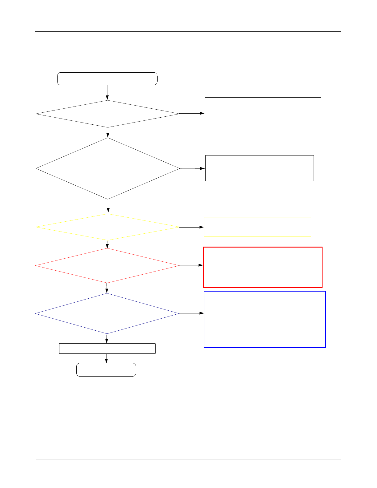
8-3-1.
Power On
Mobile phone does not power on.
Check the Battery Voltage
it more than
Is
Yes
Power-on the phone and
check the power-on sound
or motor Vibration.
Sound or Vibration is ok
No
Check the TAC1000
soldering crack, open, etc)
(
3.8
V?
.
?
No
Yes
Abnormal
If its voltage level is extremely low(under
Change the TAC1000(Power-key switch)
Charging the battery by TA.
Change the battery.
Change the FRONT-LCD ASSY
And retry to the power-on operation.
3.0
V),
Yes
Check the U600 output voltage
C660>1V,C661>1V)
(
Yes
Check the Clock OSC4000
Is that frequency24Mhz?
Yes
check the initial operation
Yes
END
No
No
If the output voltage is not satisfied with normal
condition, Change the U600.
Each voltage level has
※
Change the OSC4000.
Test condition(Oscilloscope setting)
※
us.div(time division)
:20.0
±10%
margin.
8-7
Confidential and proprietary-the contents in this service guide subject to change without prior notice.
Distribution, transmission, or infringement of any content or data from this document without Samsung’swritten authorization is strictly prohibited.
Level3Repair
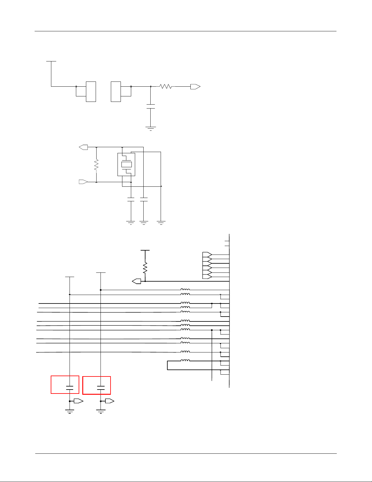
W
V_BATTERY
XTAL_24MHZ_IN
XTAL_24MHZ_OUT
VINT_1.0V_AP
ANT701
1
1
2
2
R4008
VMIF_1.0V_AP
ANT702
1
1
2
2
OSC4000
1
2
AP_N_RST_IN
C756
4
3
C4001
C4000
VCC_1.8V_AP
7
0
6
R
R718
VARM_1.0V_AP_SNSN
VARM_1.0V_AP_SNSP
VINT_1.0V_AP_SNSN
VINT_1.0V_AP_SNSP
VG3D_1.0V_AP_SNSN
VG3D_1.0V_AP_SNSP
L600
L601
L602
L613
L603
L604
L605
L606
L607
L608
L609
L610
ON_S
H4
PWRHOLD
E7
PWRON
F3
RS2N
G3
RS2P
L6
RS3N
L7
RS3P
L5
RS4N
L4
RS4P
F5
RSOB
B1
SW1
M7
SW3
N7
SW3
M4
SW4
N4
SW4
A4
SW5
B4
SW5
N10
SW6
N12
SW7
A12
SW8
B12
SW8
M1
SW10
F1
SW21
F2
SW21
J1
SW22
J2
SW22
A7
SW91
B7
SW91
A9
SW92
B9
SW92
C660
C661
BUCK1_GNDBUCK3_GND
8-8
Confidential and proprietary-the contents in this service guide subject to change without prior notice.
Distribution, transmission, or infringement of any content or data from this document without Samsung’swritten authorization is strictly prohibited.
Level3Repair
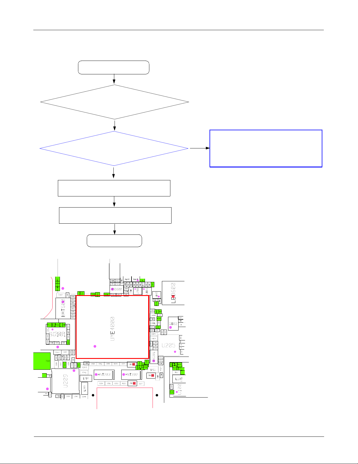
8-3-2.
Initial
Initial Failure
Yes
Re-download latest SW on the
mobile phone.
Abnormal
Re Check
Trouble shooting process
Change UME300
Change PBA
"8-3-1
Power on"
Normal
Abnormal
Abnormal
Check the OSC4000(Crack, open etc.)
Check the U600(Crack etc)
END
8-9
Confidential and proprietary-the contents in this service guide subject to change without prior notice.
Distribution, transmission, or infringement of any content or data from this document without Samsung’swritten authorization is strictly prohibited.

Level3Repair
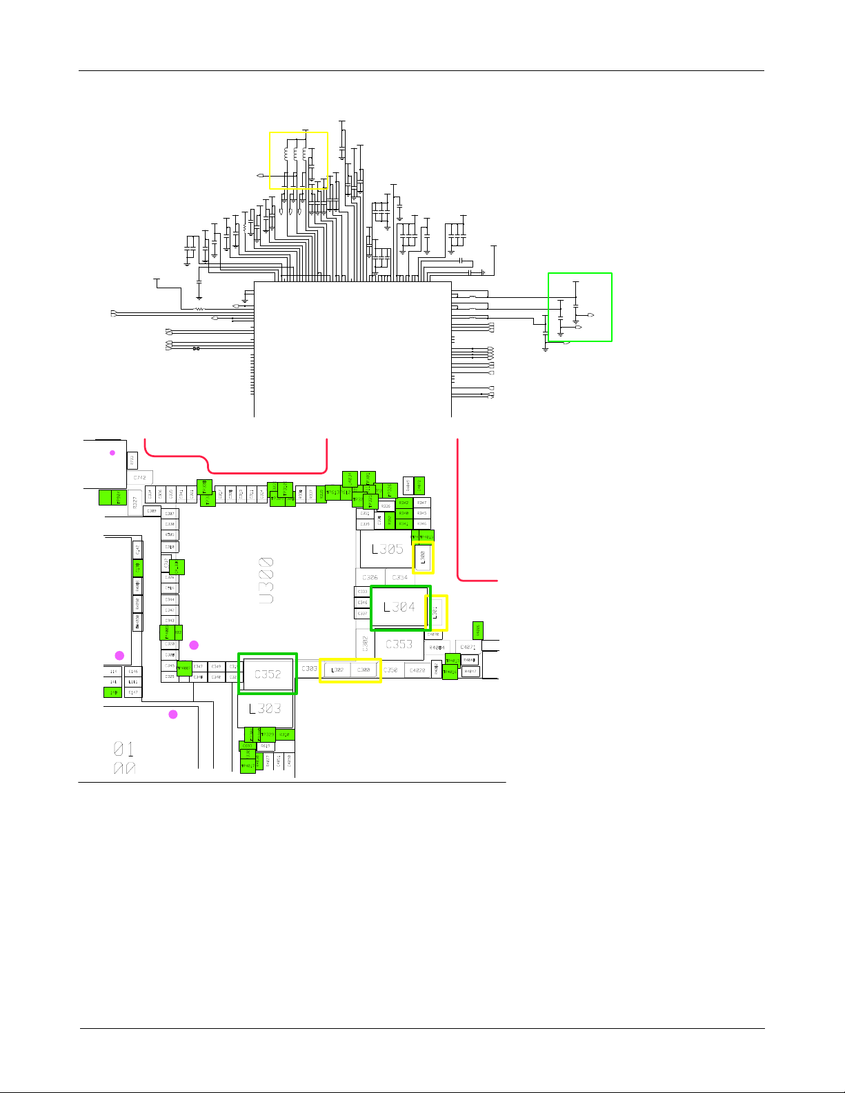
8-3-3.
No Service
No service
Yes
Check memu setting
Menu→applications→setting→wireless and network
mobile networks→network mode→setting is auto mode
Menu→Phone→Keypad
*#1234#
L300,L301,L302,C300
check Phone version
→
PHONE:N900XXXX or
PHONE:unknown
Check the CP V_BAT
→
→
PHONE:unknown
=3.6~4V
→
?
PHONE:N900XXXX
No
Check the contact of antenna.
Sub FPCB)
(
Replace the L300,L301,L302,C300
Yes
Check the CP_VSD1_, CP_VSD2_
CP_VSD1(C352)
CP_VSD2(C353)
Change the board
=0.9~1.4V
=1.8V
Abnormal
Yes
END
No
Replace the UCP300
8-10
Confidential and proprietary-the contents in this service guide subject to change without prior notice.
Distribution, transmission, or infringement of any content or data from this document without Samsung’swritten authorization is strictly prohibited.
RESET_REQ_N
RESET_PWRDWN_N
VRTC_1.8V
SPEECH_PCM_IN
SPEECH_PCM_CLK
SPEECH_PCM_OUT
SPEECH_PCM_SYNC
CP_DUMP_INT
8
9
3
3
3
3
C
C
R305
RESET_RFE_N
R310
VUSB_PD_
Level3Repair
CP_VSIM_
V_BAT
VPLL_
0
1
3
C
9
2
Y
Y
2
D
S
_
N
I
V
_
D
D
V
VUSB_IO_
VDIGRF_
7
1
3
C
1
5
2
V
U
U
1
1
U
D
D
M
S
S
P
_
_
_
N
N
I
I
N
I
V
V
V
_
_
_
D
D
D
D
D
D
V
V
V
2
1
3
C
CP_VSD2_
3
7
1
0
3
3
C
C
8
6
7
8
4
7
1
1
1
1
1
F
F
C
C
A
G
L
2
1
C
D
A
L
_
V
T
P
N
L
P
1
_
R
A
L
_
_
_
B
_
P
X
D
S
D
B
_
T
D
D
U
S
_
D
V
_
V
Y
U
D
D
_
H
V
D
D
P
V
D
M
V
_
D
D
V
U300
CP_VSD3_
CP_VSD2_
VPLL_
1
0
3
C
1
1
3
8
CP_VSD2_
0
C
3
C
0
2
CP_VSD1_
3
5
6
4
C
2
2
2
3
3
3
C
C
C
CP_VSD2_
CP_VSD2_
5
4
3
3
3
3
C
C
5
4
3
C
9
8
7
4
4
4
3
3
3
C
C
C
0
2
3
1
6
7
5
1
1
1
1
1
1
J
L
D
A
B
M
I
2
1
2
C
B
P
I
V
M
M
S
M
I
I
1
M
U
S
S
M
_
_
_
_
_
_
X
O
O
I
O
O
O
I
R
I
I
I
_
_
_
_
_
_
Y
D
D
D
D
D
H
D
D
D
D
D
P
V
V
V
V
V
M
_
D
D
V
4
5
8
5
6
4
7
2
3
8
5
3
6
2
6
1
1
1
1
1
L
C
D
C
C
D
D
A
D
H
H
K
C
C
C
M
8
8
8
8
8
2
8
C
C
C
N
G
N
N
C
C
C
I
I
I
I
I
I
I
I
I
V
V
V
V
V
V
V
1
1
M
_
_
E
_
C
C
I
I
O
S
I
M
_
H
E
_
D
_
D
O
O
I
I
V
_
_
D
D
D
D
V
V
3
A
1
1
1
1
A
A
1
M
M
_
M
M
M
_
_
_
_
_
E
E
E
M
M
M
E
E
E
_
_
O
O
O
O
O
_
_
_
_
_
_
R
I
I
I
I
I
L
L
L
O
E
O
E
E
_
_
_
_
_
O
I
I
L
L
L
R
R
R
_
D
D
_
D
D
D
C
D
D
D
O
O
O
D
D
_
D
D
D
D
D
_
_
_
C
C
C
D
V
V
V
V
D
D
V
D
D
D
_
_
_
V
D
V
D
D
D
D
D
D
V
V
V
V
D
D
D
V
V
V
CP_VSD1_
CP_VSD3_
6
3
3
C
3
1
4
2
4
4
4
4
USB_VBUS_CP_
3
3
3
3
C
C
C
C
C346
RXDATANLANE1
RXDATANLANE2
RXDATAPLANE1
RXDATAPLANE2
DSP_AUDIO_IN1
C350
U4
SD1_FB
V1
SD1_SW
V2
L303
SD1_SW
V4
SD2_FB
Y3
SD2_SW
Y4
L304
SD2_SW
V10
SD3_FB
Y10
L305
SD3_SW
E12
CC1_CLK
F13
CC1_IO
G13
CC1_RST
F14
CC2_CLK
G14
CC2_IO
H16
CC2_RST
J18
M18
K18
L18
H17
TXDATAN
H18
TXDATAP
U15
T_OUT0
T15
T_OUT1
R15
T_OUT2
P15
T_OUT3
W14
U11
ON
H11
I2S2_WA1
U8
TP307
TP308
TP309
TP310
TP311
SIM_CLK
SIM_IO
SIM_RST
RFE_MPHY_RX1_DATX
RFE_MPHY_RX2_DATX
RFE_MPHY_RX1_DAT
RFE_MPHY_RX2_DAT
RFE_MPHY_TX_DATX
RFE_MPHY_TX_DAT
HW_ID4_CP
DSP_AUDIO_IN1
CP_ON
GPS_CLK_EN
CP_VSD1_
CP_VSD2_
CP_VSD3_
C354
C352
C353
VSD1_GND
VSD2_GND
VSD3_GND
3
5
1
6
8
6
7
1
1
1
Y
Y
H
W
J
B
H
P
S
P
N
G
G
3
3
C
T
T
U
_
_
V
S
B
S
E
E
B
V
B
_
R
R
_
P
P
O
O
C
C
C
C
V
V
_
_
D
D
D
D
V
V
V_BAT
0
2
1
0
0
0
3
3
3
L
L
L
0
0
3
VSD2
CP_VSD2_
VDIGRF_
VPLL_
CP_VSD2_
VRTC_
CP_VSIM_
VUSB_IO_
7
3
3
C
0
4
3
C
1
5
3
C
RESET_N_RF
TP305
9
1
1
3
2
C
3
C
8
2
2
5
3
3
C
R
0
3
3
3
3
3
C
C
J13
RCT_MON1
J14
RCT_MON2
TP301
N17
XRESET_N
P10
RESET_ALL
P7
RESET_BB_N
P9
OFF_N
P12
TP304
RESET_RFE_N
H14
RESET2_N
N15
MMCI1_CD
N14
MMCI1_CLK
N12
MMCI1_CMD
K13
MMCI1_DAT_0
N10
MMCI1_DAT_1
L12
MMCI1_DAT_2
N11
MMCI1_DAT_3
L5
NAND_ADQ_0
N2
NAND_ADQ_1
J3
NAND_ADQ_2
K4
NAND_ADQ_3
K7
NAND_ADQ_4
L7
NAND_ADQ_5
L3
NAND_ADQ_6
J8
NAND_ADQ_7
K5
NAND_ADQ_8
H4
NAND_ADQ_9
J6
NAND_ADQ_10
N4
NAND_ADQ_11
M4
NAND_ADQ_12
F3
NAND_ADQ_13
H5
C
VRTC_
VUSB_PD_
3
2
6
0
0
0
3
3
3
C
C
C
9
0
3
C
D
D
D
6
1
N
N
N
3
G
G
G
C
_
_
_
3
2
1
D
D
D
S
S
S
V
V
V
2
3
3
2
8
7
1
1
2
2
6
8
1
1
1
1
P
P
V
Y
R
R
W
W
Y
Y
W
M
2
1
F
F
2
3
L
P
C
U
D
A
O
I
L
E
R
D
P
D
T
M
M
P
M
N
I
I
_
P
R
S
V
S
_
R
G
P
A
S
S
I
B
V
_
V
V
B
V
_
V
V
V
S
D
_
N
S
B
I
U
V
D
U
S
V
V
D
V
_
U
V
V
D
D
V
8-11
Confidential and proprietary-the contents in this service guide subject to change without prior notice.
Distribution, transmission, or infringement of any content or data from this document without Samsung’swritten authorization is strictly prohibited.

Level3Repair
8-3-4.
Sim Part
Insert SIM card
Yes
Is SIM/SD socket ok?
Yes
Check the SIM Voltage.
C694 or C695 of SIM
(
FPCB)
>= 1.8or3.0?
Yes
END
No
No
Replace SIM/SD socket.
Change to the new SIM card.
If it doesn`t still work SIM card after changing
the SIM card, Check the U300(Crack etc)
8-12
Confidential and proprietary-the contents in this service guide subject to change without prior notice.
Distribution, transmission, or infringement of any content or data from this document without Samsung’swritten authorization is strictly prohibited.

Level3Repair
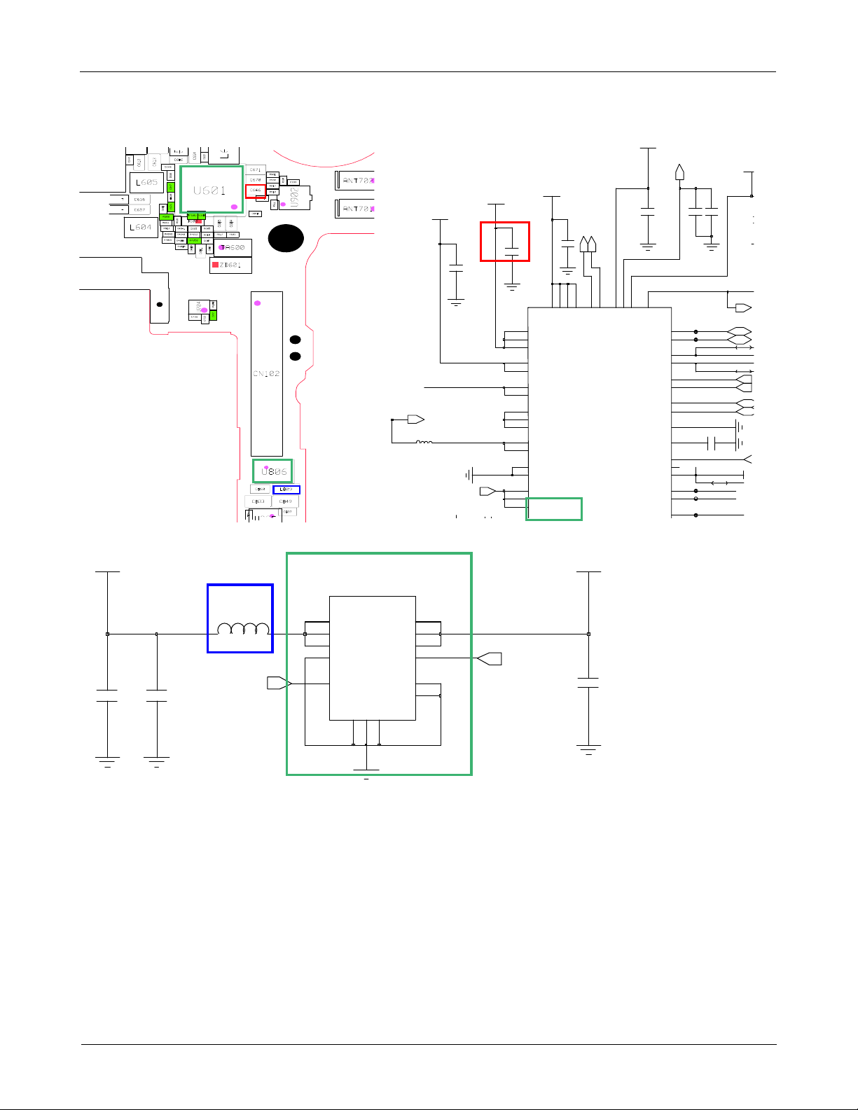
8-3-5.
Charging Part
TA/USB Insert
Charging Sequence Start
Check the CHG_IN_5V(C666)=5V
Battery is Charging?
VBUS_5V
Yes
Yes
Yes
Yes
=5V
No
No
No
Check L809=5V,
or may not connected TA/USB
Resolder and Replace U806
Resolder or Replace U601
END
8-13
Confidential and proprietary-the contents in this service guide subject to change without prior notice.
Distribution, transmission, or infringement of any content or data from this document without Samsung’swritten authorization is strictly prohibited.
Level3Repair
C
6
6
7
A
T
V
U
U
V
V
WPC_5V
PM_SYS_PWR
CIG22E1R0MNE
PM_SYS_PWR
E
D
8
H
G
F
_
T
T
A
B
COMN1
COMP2
MIC_USB
_
S
U
B
V
A8
DN1
A9
DP2
E8
UT1
D8
UR2
E10
SL1
D10
SR2
B10
C10
C9
BC
C8
0603
NC
B9
UID
D9
IDB
C6
JIG
B7
ADN1
A7
ADP2
D7
AUR2
2
6
6
C
TP608
TP609
TP610
TP611
TP613
3
6
6
C
C676
V_B
VCC_1.8V_AP
E
S
E
N
CHG_IN_5V
8
6
6
C
V_BATTERY
6
6
6
C
C1
CHGIN
D1
CHGIN
D2
CHGIN
B2
WCIN
B1
WCIN
E1
BYP
E2
BYP
C2
BYP_W
C3
BYP_W
D3
BYP_W
F1
CHGLX
G1
CHGLX
H1
CHGPG
J2
CHGPG
H4
SYS
J3
SYS
J4
SYS
S
E
N
S
E
_
S
Y
_
C665
R
D
E
N
T
G
T
T
A
A
B
B
_
V
V
4
6
6
C
5
H
T
T
A
B
3
6
2
7
9
8
6
5
J
J
H
T
T
T
T
T
T
A
A
A
B
B
B
E
H
H
C
B
T
S
P
O
N
I
A
U
S
S
V
_
_
B
B
M
T
T
V
V
A
A
M
M
B
B
U601
V_BUS_5
C849
C837
L809
OVP_EN
CHG_IN_5
U806
B3
IN
C2
IN
C3
IN
C1
OVLO
A1
_EN\
VBUSDET
D
D
N
N
G
G
4
4
4
C
A
B
A2
OUT
A3
OUT
B2
OUT
B1
1
NC
2
NC
D
N
G
VBUS_DET
C860
8-14
Confidential and proprietary-the contents in this service guide subject to change without prior notice.
Distribution, transmission, or infringement of any content or data from this document without Samsung’swritten authorization is strictly prohibited.
Level3Repair
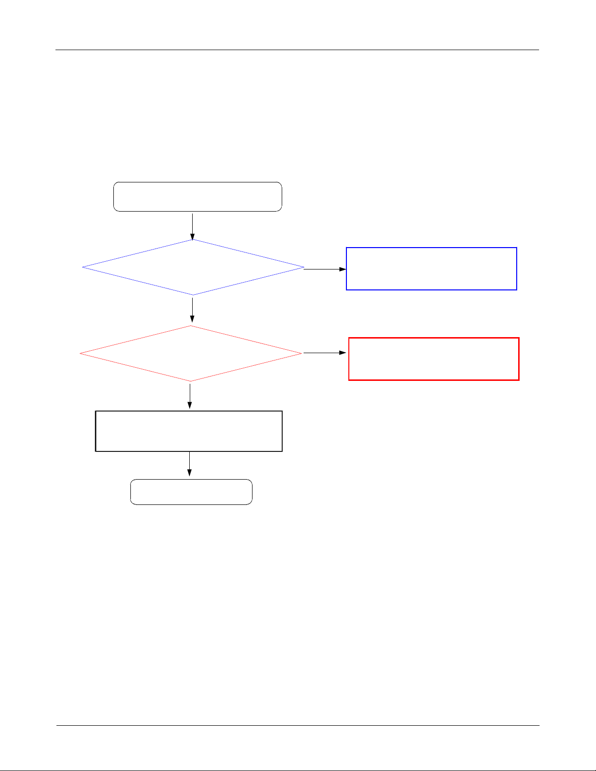
8-3-6.
OTG
OTG does not work
Yes
Check CHG_IN_5V(C666)=5V
Yes
Check VBUS_5V(L809)
=5V
No
No
Check U601
Check U806
Yes
Change the board
Yes
END
8-15
Confidential and proprietary-the contents in this service guide subject to change without prior notice.
Distribution, transmission, or infringement of any content or data from this document without Samsung’swritten authorization is strictly prohibited.

Level3Repair
V_BUS_5V
C849
C837
L809
OVP_EN
VCC_1.8V_AP
VBUS_DET
V_BATTERY
CHG_IN_5V
WPC_5V
C668
CAP X2
C671
C670
V_BAT
PM_SYS_PWR
L614
VCC_1.8V_AP
R609
C685
AP_JTAG_EXTRST
PM_SYS_PWR
R610
VCC_3.0V_MOTOR
VIBTONE_PWM
VF
MOTOR_P
MOTOR_N
C617
C673
PM_SYS_PWR
LED600
C672
CAM_FLASH_SET
CAM_FLASH_EN
C684
R615
C686
VCC_1.8V_AP
IF_PMIC_SDA
IF_PMIC_SCL
nPOWER
C687
VCC_1.8V_AP
VBUS_DET
CHG_IN_5V
C860
PMIC_ACO KB
W_CHG_DET
USB_VBUS_AP_4. 9V
USB_VBUS_C P_4.9V
U806
B3
A2
IN
OUT
C2
A3
IN
OUT
C3
B2
IN
OUT
C1
B1
OVLO
VBUSDET
A1
1
_EN\
NC
2
NC
GND
GND
GND
C4
A4
B4
VBATGND_SENSE
V_BATTERY_SENSE
C664
C666
J6
H6
H2
H3
B8
MVIO
BATTJ5BATT
BATTH5BATT
BAT_SP
BAT_SN
C1
CHGIN
D1
CHGIN
D2
CHGIN
B2
WCIN
B1
WCIN
E1
BYP
E2
BYP
C2
BYP_W
C3
BYP_W
D3
BYP_W
F1
CHGLX
G1
CHGLX
H1
CHGPG
J2
CHGPG
H4
SYS
J3
SYS
J4
SYS
U601
G2
C678
AVL
F3
DETBATB
F2
INOKB
E3
WCINOKB
A5
FLED1
A6
FLED1
B5
TORCHEN
B6
FLASHEN
A2
SAFEOUT1
A3
SAFEOUT2
H9
IN_MOT
H10
MDN
J9
MDP
G9
MGAIN
G10
MPWM
F6
VIO
G6
SDA
F9
SCL
D5
MRST1B
D4
INTB
D6
RESETB
GNDFG
GND_AG4GND_A
GNDM
GND_Q
GND_D
J8
E4
E6
G5
F10
V_BAT
C665
C663
C662
C667
E9
C7
MVBAT
MVBUS
C669
H8
V_BATTERY_SENSE
A8
TP608
BATT_FG
DN1
USB2_AP_D-
TP609
A9
DP2
USB2_AP_D+
E8
UT1
D8
UR2
E10
SL1
D10
SR2
B10
COMN1
C10
COMP2
C9
BC
C8
MIC_USB
B9
UID
D9
IDB
C6
JIG
B7
ADN1
A7
ADP2
D7
AUR2
E7
AUT1
H7
QSTRT
G8
VCELL
F8
EO
J7
ALRTB
G7
SCLFG
F7
SDAFG
B3
TEST1
C4
TEST2
A4
TEST3
B4
TEST4
C5
VCCTEST
F4
SYS_A
F5
SYS_A
G3
OVPENB
E5
VBUSDET
A1
NC
A10
NC
J1
NC
J10
NC
1
NC
2
NC
JTAG_TXD
AP_TXD
AP_RXD
JTAG_RXD
VPS_L
VPS_R
MUIC_DM
MUIC_DP
C676
D600
MUIC_ID
PMIC_JIGONB
JTAG_IF_CON_SENSE
TP610
USB_D_M
TP611
USB_D_P
TP613
CP_RXD_1.8V
TP612
CP_TXD_1.8V
V_BATTERY_SENSE
FUEL_SCL_1.8V
FUEL_SDA_1.8 V
PM_SYS_PWR
R626
OVP_EN
VBUS_DET
C697
OVP_EN
VCC_1.8V_AP
R613
4.7K
0603
FUEL_ALERT
R617
IF_PMIC_IRQ
8-16
Confidential and proprietary-the contents in this service guide subject to change without prior notice.
Distribution, transmission, or infringement of any content or data from this document without Samsung’swritten authorization is strictly prohibited.

Level3Repair
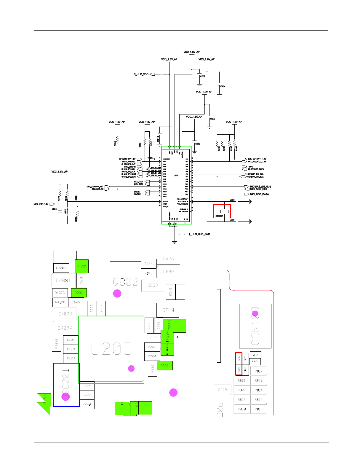
8-3-7.
Sensor
Sensor does not work
Yes
Check OSC201
Frequency
Check R201, R202
= 32.768
Yes
I2C is OK?)
(
Yes
Replace Sensor IC
khz
?
No
No
Replace OSC201
Replace U 205
END
Yes
8-17
Confidential and proprietary-the contents in this service guide subject to change without prior notice.
Distribution, transmission, or infringement of any content or data from this document without Samsung’swritten authorization is strictly prohibited.
Level3Repair
8-18
Confidential and proprietary-the contents in this service guide subject to change without prior notice.
Distribution, transmission, or infringement of any content or data from this document without Samsung’swritten authorization is strictly prohibited.
Level3Repair
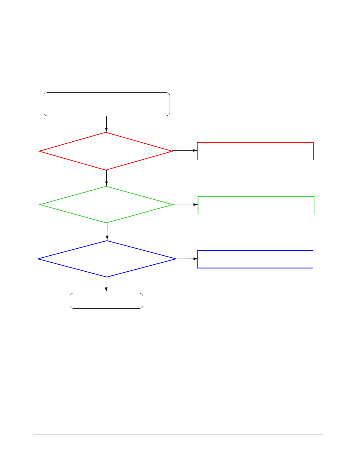
8-3-8-1
Microphone Part
Check main microphone function
in voice call Handset mode or voice recorder mode
Check sub board
connection(HDC900)
Check the voltage at
C1020
- Main MIC
Yes
Yes
=2.8V
No
No
Set the HDC900 connection
resolder or replace U1001
Yes
Check component soldering
statuses of L909, L910
Yes
END
No
Resolder or replace L909, L910
8-19
Confidential and proprietary-the contents in this service guide subject to change without prior notice.
Distribution, transmission, or infringement of any content or data from this document without Samsung’swritten authorization is strictly prohibited.

Level3Repair
N
N
MAIN_MICBIAS_EN
MAIN_MICBIAS_2.8VV_BAT
U704
4
VDD
3
CE
1
VOUT
2
GND
D
N
G
5
C733C732
C863
L816
C864
L817
MAIN_MIC_N_CON
MAIN_MIC_P_CON
8-20
Confidential and proprietary-the contents in this service guide subject to change without prior notice.
Distribution, transmission, or infringement of any content or data from this document without Samsung’swritten authorization is strictly prohibited.

Level3Repair
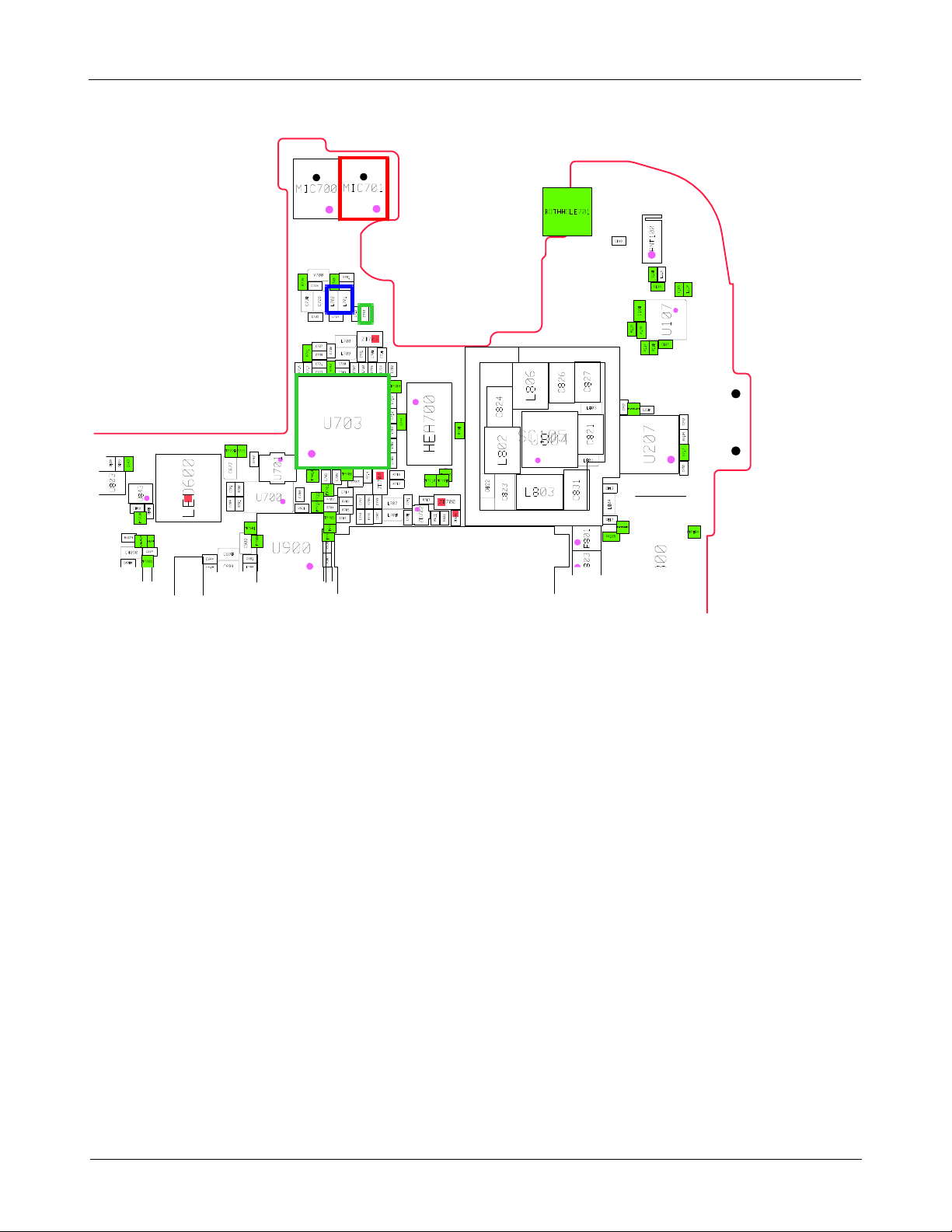
8-3-8-2.
Microphone Part-Sub(2nd) MIC
Check Sub(2n d) microphone function
in voice call loudSPK NS Off mode
or in camcording mode
Yes
Check PC B where Sub MIC
MIC701) is placed
(
for any damage
Yes
Check the voltage at
C753
=2.8V
No
No
Replace the PCB module
resolder or replace U703
Yes
Check component soldering
statuses of L701, L702
Yes
END
No
Resolder or replace L701, L702
8-21
Confidential and proprietary-the contents in this service guide subject to change without prior notice.
Distribution, transmission, or infringement of any content or data from this document without Samsung’swritten authorization is strictly prohibited.

Level3Repair
D
SUB_MICBIAS_2.8V
1
0
7
V
MAIN_MIC_N
MAIN_MIC_P
MIC701
L701
1
OUT
OUT
GND1
GND
GND2
GND
GND3
GND
VDD5VDD
2
3
4
C736
C737
L702
SUB_MIC_P
SUB_MIC_N
0
4
7
R
VCC_1.8V_AP
VCC_1.8V_AP
V_BAT
7
8
A
A
2
1
D
D
D
D
V
V
O
O
I
I
U703
D
D
N
N
G
G
D
D
9
1
9
F
A
B
V_BAT
C702
C703
C706
C708
0
1
1
2
4
1
3
1
1
1
1
J
L
H
G
C
J
G
G
L
E
D
R
D
A
D
D
D
D
D
D
D
D
O
D
D
V
V
D
O
V
V
D
V
P
V
L
A
D
D
A
P
L
C
L
P
O
O
L
S
S
D
D
L
L
D
L
N
D
D
D
D
D
G
D
N
N
N
N
N
A
N
G
G
G
G
G
L
P
P
P
G
P
L
P
P
H
H
H
S
D
C
1
1
8
5
6
7
J
J
L
L
B
K
P
L
D
N
G
P
S
1
1
1
L
K
LINEOUT1L|LINEOUT1P
LINEOUT1R|LINEOUT1N
LINEOUT2L|LINEOUT2P
LINEOUT2R|LINEOUT2N
R
R
D
D
N
N
G
G
P
P
S
S
1
1
1
L
F4
TEST
A4
CLKI0
A3
CLKI1
F2
TP702
RTCI
E1
SCL
E2
SDA
F11
VREF
G9
VREF2
L4
C712
CPP
K5
CPN
K4
REFCPP
L6
REFCPN
K2
SPOUTLN
L2
SPOUTLP
K10
SPOUTRN
L10
SPOUTRP
K9
RCOUTP
J10
RCOUTN
D2
IRQ_N
H3
DETIN
J8
DETIN_HP
L9
HPDET
K8
MICDET
E9
MBS4
C11
MIG4
C10
MIN4
K6
HPOUTL
L7
HPOUTR
K7
HSENSE
C722
H10
H11
H9
J9
C
C
N
N
2
XTAL_24MHZ_AP
CODEC_CLK32K
C710
C714
C715
SPK_OUT_N
SPK_OUT_P
RCV_P
RCV_N
EAR_MIC_N
EAR_MIC_P
C718
EAROUT_L
EAROUT_R
EAROUT_FB
VPS_L
VPS_R
C724
G_DET
L_DET
EAR_IMP_DET
EAR_ADC_3.5
VCC_1.8V_AP
R708
EAR_SEND_EN
VCC_1.8V_AP
YMU_LDO_EN
R702
C705
C707
C709
1
1
1
2
8
1
B
D
G
B
E
0
D
D
D
D
D
D
O
O
O
D
V
D
D
D
V
A
L
L
L
|
|
|
O
I
D
D
D
D
D
D
V
V
V
D
D
D
B5
PA0|DMCK
A6
TP701
YMU_SPI_SCK
YMU_SPI_MOSI
YMU_SPI_MISO
YMU_SPI_SS_N
MM_I2S_CLK
MM_I2S_SYNC
MM_I2S_DO
MM_I2S_DI
SPEECH_PCM_CLK
SPEECH_PCM_SYNC
SPEECH_PCM_OUT
SPEECH_PCM_IN
BT_PCM_CLK
BT_PCM_SYNC
BT_PCM_OUT
BT_PCM_IN
1
4
7
R
SUB_MICBIAS_2.8V
3RD_MICBIAS_2.8V
C752
C753
SUB_MIC_P
SUB_MIC_N
3RD_MIC_P
3RD_MIC_N
R704
R705
R707
TP704
TP705
TP706
TP708
TP709
TP710
C716
C717
C719
C720
C721
C723
PA1|DMDIN0
B6
PA2|DMDIN1
C2
SBCK
B3
SBD
E4
IFSEL
D3
R703
SCK
E3
MOSI
G3
MISO
G4
SPIMODE
F3
SS_N
A5
TP703
BCLK0
B4
LRCK0
C3
SDIN0
C4
SDOUT0
C5
TP707
BCLK1
D5
LRCK1
D4
SDIN1
C6
SDOUT1
C7
BCLK2
D6
LRCK2
B7
SDIN2
D7
SDOUT2
E10
MBS1
A10
MIN1
A11
MIN1
B10
MIG1
F10
MBS2
D10
MIN2
D9
MIG2
F9
MBS3
C9
MIN3
B11
MIG3
E8
LINEINL|LINEINP
F8
LINEINR|LINEINN
D
D
D
D
D
D
D
D
D
D
N
N
N
N
N
N
N
N
N
N
G
G
G
G
G
G
G
G
G
G
A
A
A
A
A
A
A
D
A
D
1
1
2
2
3
1
3
2
5
4
1
J
J
J
J
A
K
H
H
A
D
8-22
Confidential and proprietary-the contents in this service guide subject to change without prior notice.
Distribution, transmission, or infringement of any content or data from this document without Samsung’swritten authorization is strictly prohibited.
Level3Repair
8-23
Confidential and proprietary-the contents in this service guide subject to change without prior notice.
Distribution, transmission, or infringement of any content or data from this document without Samsung’swritten authorization is strictly prohibited.
 Loading...