Samsung SP-C500R Service Manual [ENG]

SERVICE MANUAL
SP-C500R
PRINTEDINMAY2003

CONTENT
1. SERVICE GUIDE
2. SPECIFICATIONS
3. TROUBLESHOOTING FLOWCHART
4. TEST MODE / ALIGNMENT
5. PART LIST
6. BLOCK DIAGRAM
7. EXPLODE VIEW
8. REFERENCE MAP
9. CIRCUIT DESCRIPTION
10. CIRCUIT PATH
11. CIRCUIT DIAGRAM
12. APPENDIX

1. SERVICE GUIDE
1. When adjusting cordless phone it is highly recommanded that it should be done in the
shielded room to prevent adjustment from interference.
2. When measuring RF part, use 50 Ω standard coaxial cables.
3. For adjustment of RF coil, use ceramic adjustment driver.
Metalic driver may cause not only demage of core and coil but also change of coil's
characteristics.
4. Use proper screw drivers to prevent screws from demage.
2. SPECIFICATIONS
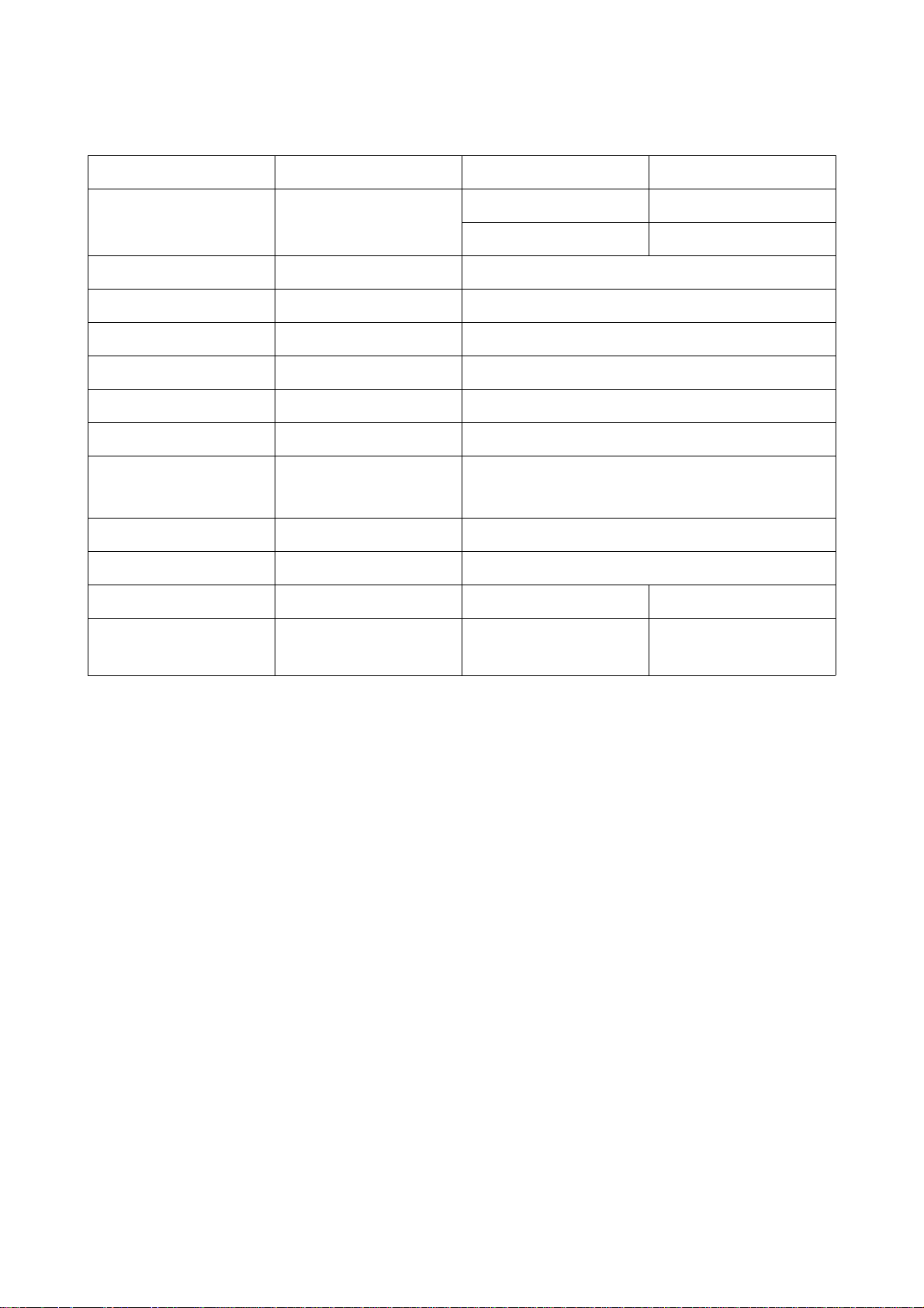
Spec Uint Handset Base unit
DC 3.6V,350mAh DC9V,300mA/150mA
Power Supply V/mA
Re-charging Battey Adaptor 220V
Frequency MHz 814.0125~814.9875 / 903.0125~903.9875
Channel Number 40
Channel Spacing kHz 25
Output Power mW 10
Bandwidth kHz 16
Receiving Sensitivity uV 2
Operation Time hour
Operating Temperature °C 0~55
Operating Humidity % 5~90
Weight g 202 148
Size
mm 105x75x115 50x25x175
(widthxlengthxheight)
stand-by : 20 hour
talk: : 3 hour
3. TROUBLESHOOTING FLOWCHART
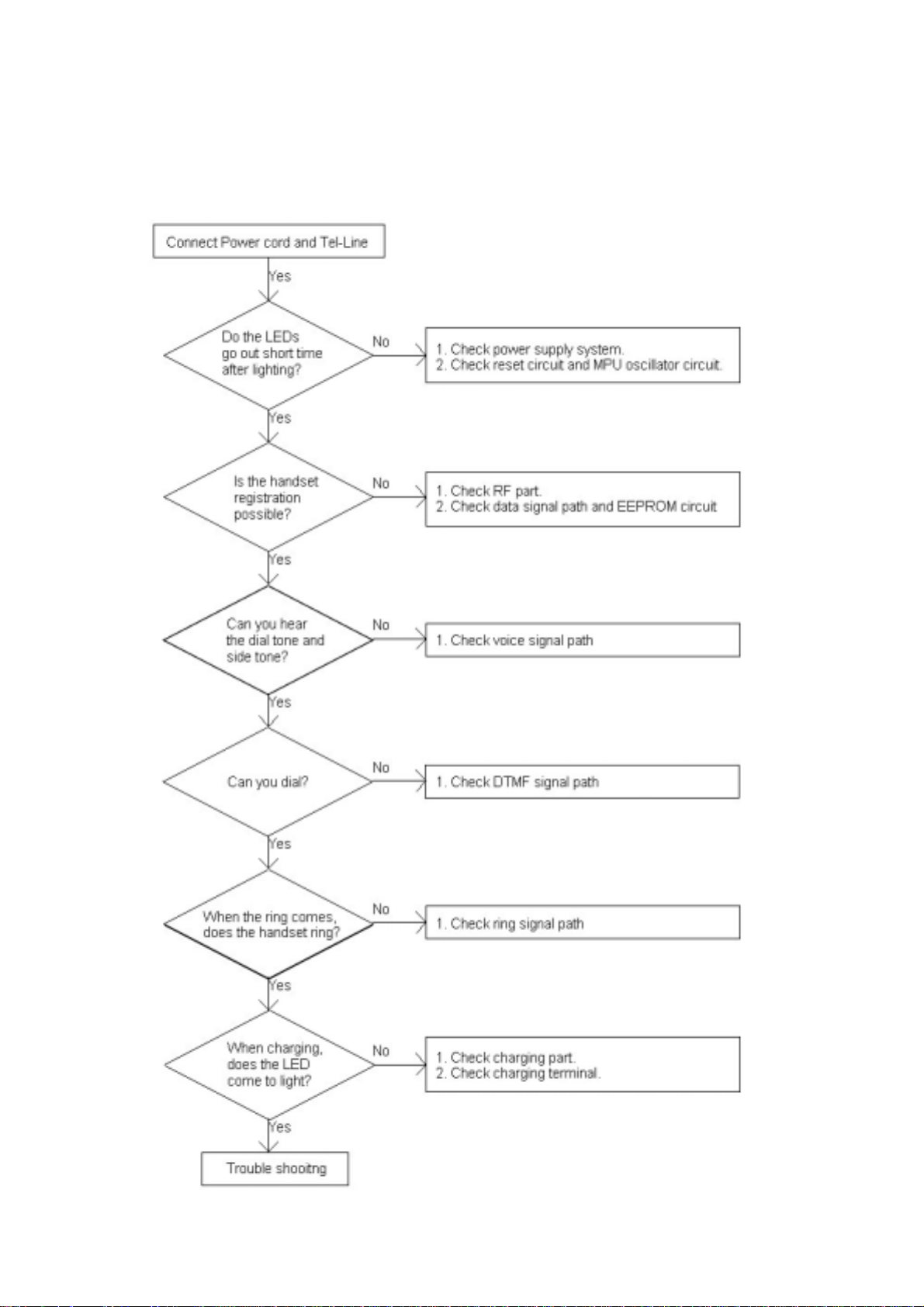
3.1 BASE UNIT
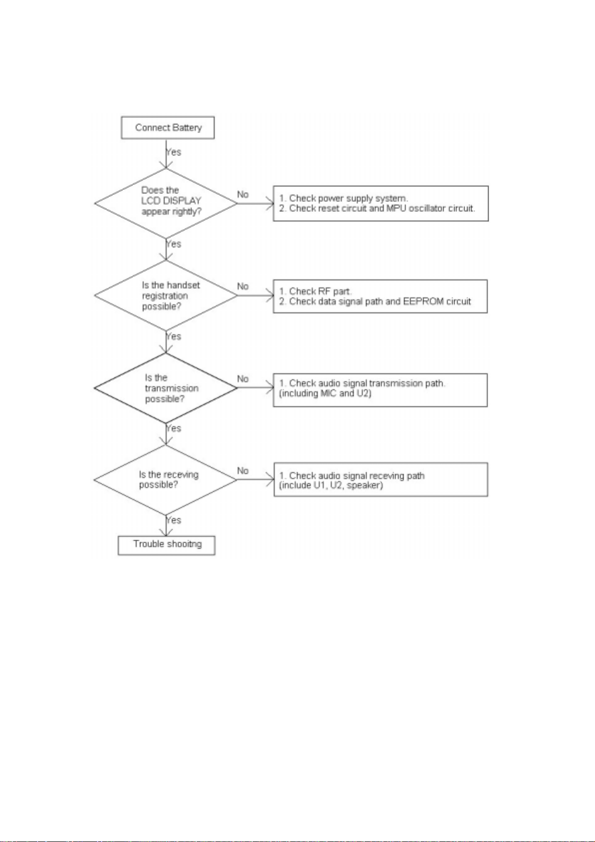
3.2 HANDSET
4. TEST MODE
4.1 BASE UNIT
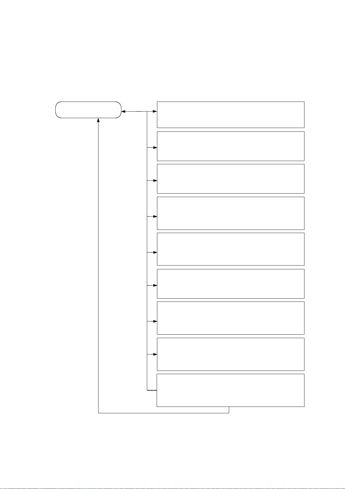
- How to start Test Mode
Powe ON with holding paging button.
After about 2 second, TEST MODE starts.
TEST MODE START
"TX / RX TEST MODE (20CH)"
(Nomal Test condition)
Set TM_SW 0,1,2,3 to 1,1,1,0 respectively
Press paging key.
"TX TEST MODE"
Set TM_SW 0,1,2,3 to 1,1,0,0 respectively
Press paging key..
"TX DATA TEST MODE"
Set TM_SW 0,1,2,3 to 1,1,0,1 respectively
Press paging key.
"RX TEST MODE"
Set TM_SW 0,1,2,3 to 0,0,0,0 respectively
Press paging key.
"DTMF TEST" (precede 1 to # by pressing key)
Set TM_SW 0,1,2,3 to 1,0,1,1 respectively
Press paging key.
"Channel is increased by 1."
Set TM_SW 0,1,2,3 to 0,1,1,1 respectively
Press paging key.
"Channel is increased by 5."
Set TM_SW 0,1,2,3 to 0,0,1,1 respectively
Press paging key.
"Channel is decreased by 5."
Set TM_SW 0,1,2,3 to 1,1,1,1 respectively
Press paging key.
" TEST MODE RESTART"
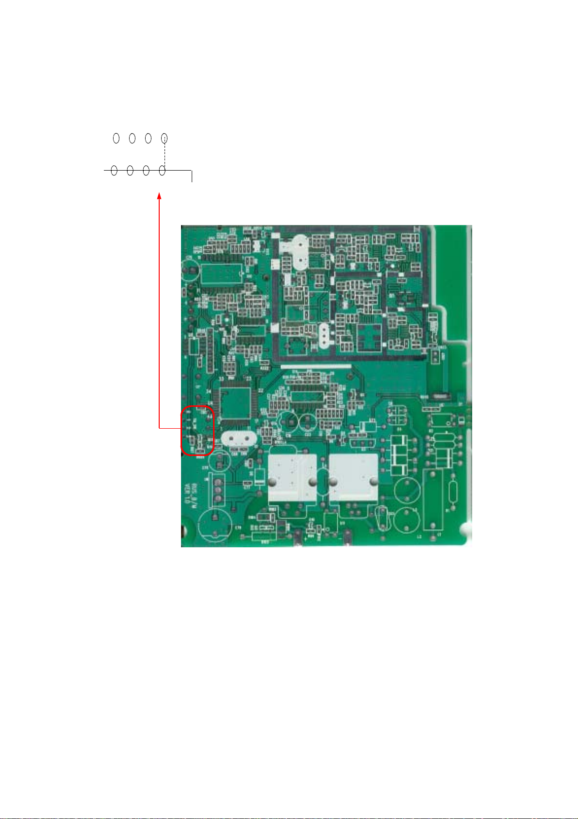
* DEFAULT TEST CHANNEL IS C H 20.
* "1"= OPEN ,"0"= SHORT in TEST MODE SWITCH
EX)
TM_SW ===> 1,1,1,0 : TX TEST MODE
01 23 GND
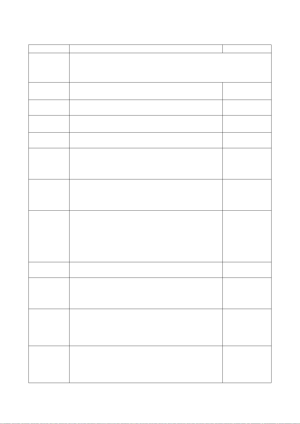
4.2 BASE UNIT ALIGNMENT
Test Item Test conditon/Test Procedure SPEC
1.Powe ON with holding paging button.
TEST MODE
TX VCO
RX VCO 1.Adjust VCO COIL (L302) to DC 2.5V at TP30 1. 2.5±0.5V
After about 2 second, TEST MODE starts.
When measuring the RF LEVEL, use 50 Ω standard coaxial cables.
2.
Defaul channel on Test Mode is CH 20.
***
1.Adjust VCO COIL (L302) to DC 2.5V at TP30 2.
2.5±0.5V
TX POWER
TX
FREQUENCY
NORMAL
DEVIATION
TX
DISTORTION
RX AUDIO
LEVEL
RX
DISTORTION
1.Set HP8920 to TX TEST MODE
2.Adjust RV201 so that the reading on HP8920 is 9.5 dBm.
1.Set HP8920 to TX TEST MODE
2.Adjust CV301 so that the reading on HP8920 is 904.4875MHz.
1.Set HP8920. AF-GEN-FREQ : 1kHz / 240mV
HPF:400Hz , LPF:15KHz
2.Connect audio output of HP8920 to Feeding bridge.
3.Adjust RV3 so that the reading on HP8920 is 3.0 KHz.
1.Set HP8920. AF-GEN-FREQ : 1kHz / 240mV
HPF:400Hz , LPF:15KHz
2.Connect audio output of HP8920 to Feeding bridge.
3.Check the reading on HP8920. No adjust.
RX TEST MODE
***
1.Set HP8920 to RX TEST MODE.
RF-GEN-FREQ:814.4875MHz
AMPLITUDE:-55dBm,
AF-GEN-FREQ:1KHz,AF_GEN
FM:3KHz ,HPF:400MHz,LPF:15KH
2.Adjust RV1 so that the reading on HP8920 is 1100mV.
1.HP8920 set up is same as RX AUDIO LEVEL
2.Adjust T301 so that distortion is minimized.
9.5±0.5dBm
904.4875MHz ±
800Hz
3.0 ±0.15 KHz
3.0% max.
-TELLINEOUT
LEVEL= 1100mV
- test point(TP8)
= 150±30mV
test point ; TP9
3.0% max.
RX S/N RATIO
RX SINAD
RSSI
1.HP8920 set up is same as RX AUDIO LEVEL.
2. filter option ; CCITT ON.
3. Selects the S/N FUNCTION and check the reading. No adjust.
1.HP8920 set up is same as RX AUDIO LEVEL.
2. filter option ; CCITT ON. AMPLITUDE:-110dBm,
HPF:400Hz,CCITT ON,
3. Selects the SINAD FUNCTION and check the reading.
No adjust
1.HP8920 set up is same as RX AUDIO LEVEL.
AMPLITUDE:-115dBm, FM MODULATION :OFF
2.Adjust RV301 so that green LED is bliking.
test point ; TP9
50dB min.
test point ; TP9
27dB min
-115dBm±1dBm
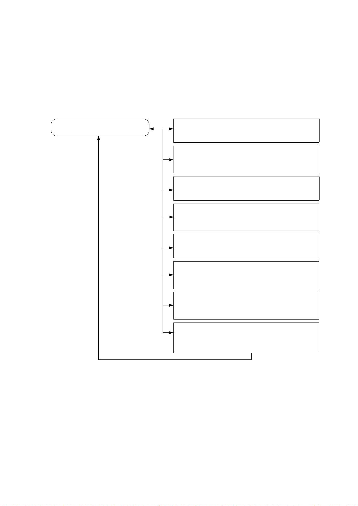
.3 HANDSET TEST MODE
4
- How to start Test Mode
Connect the battery to the handset with holding "*" and "#" button. You will hear beep sound.
Then press " * " and " # " button sequentially.
The TEST MODE starts with beep sound and you will see the channel number "20" on LCD.
TEST MODE START TX / RX TEST MODE (20CH)
(nomal test conditon)
Press the [REDIAL] button
→TX TEST MODE
Press the [TALK] button
→TX TEST MODE
Press the [VOLUME] button
→RX TEST MODE
Press the [MUTE] button
→TX MUTE MODE
Press the [ # ] button
→VOLUME CONTROL
Pressthe[*]button
→BELL VOLUME CONTROL
Press the [MEMORY] button
→
TEST MODE RESTART
* DEFAULT TEST CHANNEL IS C H 20.
* You can change the test channel by input 2 digits number between 01 and 40.
4.3.1 HANDSET ALIGNMENT
Test item Test Condition/ Procedure SPEC
Connect the battery to the handset with holding "*" and "#" button.
1
TEST MODE
TX VCO
RX VCO 1..Adjust VCO COIL (L302) to DC 1.5V at TP301. 1.5±0.4V
You will hear boop sound. Then press " * " and " # " button sequentially.
When measuring the RF LEVEL, use 50 Ω standard coaxial cables.
2.
Defaul channel on Test Mode is CH 20.
***
1.Adjust VCO COIL (L302) to DC 1.5V at TP30 2.
1.5±0.4V
TX POWER
TX
FREQUENCY
NORMAL
DEVIATION
TX
DISTORTION
RX AUDIO
LEVEL
RX
DISTORTION
RX S/N RATIO
RX SINAD
RSSI
1.Set HP8920 to TX TEST MODE
2.Adjust RV201 so that the reading on HP8920 is 9.5 dBm.
1..Set HP8920 to TX TEST MODE
2.Adjust CV301 so that the reading on HP8920 is 814.4875MHz.
1.Set HP8920. AF-GEN-FREQ : 1kHz / 21mV
HPF:400Hz , LPF:15KHz
2.Connect audio output of HP8920 to TP5.
3.Adjust RV2 so that the reading on HP8920 is 3.0 KHz.
1.Set HP8920. AF-GEN-FREQ : 1kHz / 21mV
HPF:400Hz , LPF:15KHz
2.Connect audio output of HP8920 to TP5.
3.Check the reading on HP8920. No adjust.
RX TEST MODE
***
1.Set HP8920 to RX TEST MODE.
RF-GEN-FREQ:903.4875MHz )
AMPLITUDE:-55dBm,
AF-GEN-FREQ:1KHz,AF_GEN
FM:3KHz ,HPF:400MHz,LPF:15KH
2.Adjust RV1 so that the reading on HP8920 is 100mV at TP1.
1.1.HP8920 set u p is same as RX AUDIO LEVEL
2.Adjust T301 so that distortion is minimized.
1.HP8920 set up is same as RX AUDIO LEVEL.
2. filter option ; CCITT ON.
3. Selects the S/N FUNCTION and check the reading. No adjust.
1..HP8920 set up is same as RX AUDIO LEVEL.
2. filter option ; CCITT ON. AMPLITUDE:-110dBm,
HPF:400Hz,CCITT ON,
3. Selects the SINAD FUNCTION and check the reading.
No adjust
1.HP8920 set up is same as RX AUDIO LEVEL.
AMPLITUDE:-115dBm, FM MODULATION :OFF
2.Adjust RV301 so that level transition on TP25 is repeated.
9.5±0.5dBm
814.4875MHz±
800Hz
3.0 ±0.15 KHz
3.0% max
test point (TP1)
=100mV
test point (TP2)
=130±25mV
test point ; TP9
3.0% max.
test point ; TP3
50dB min.
test point ; TP3
27dB min
-115dBm±1dBm
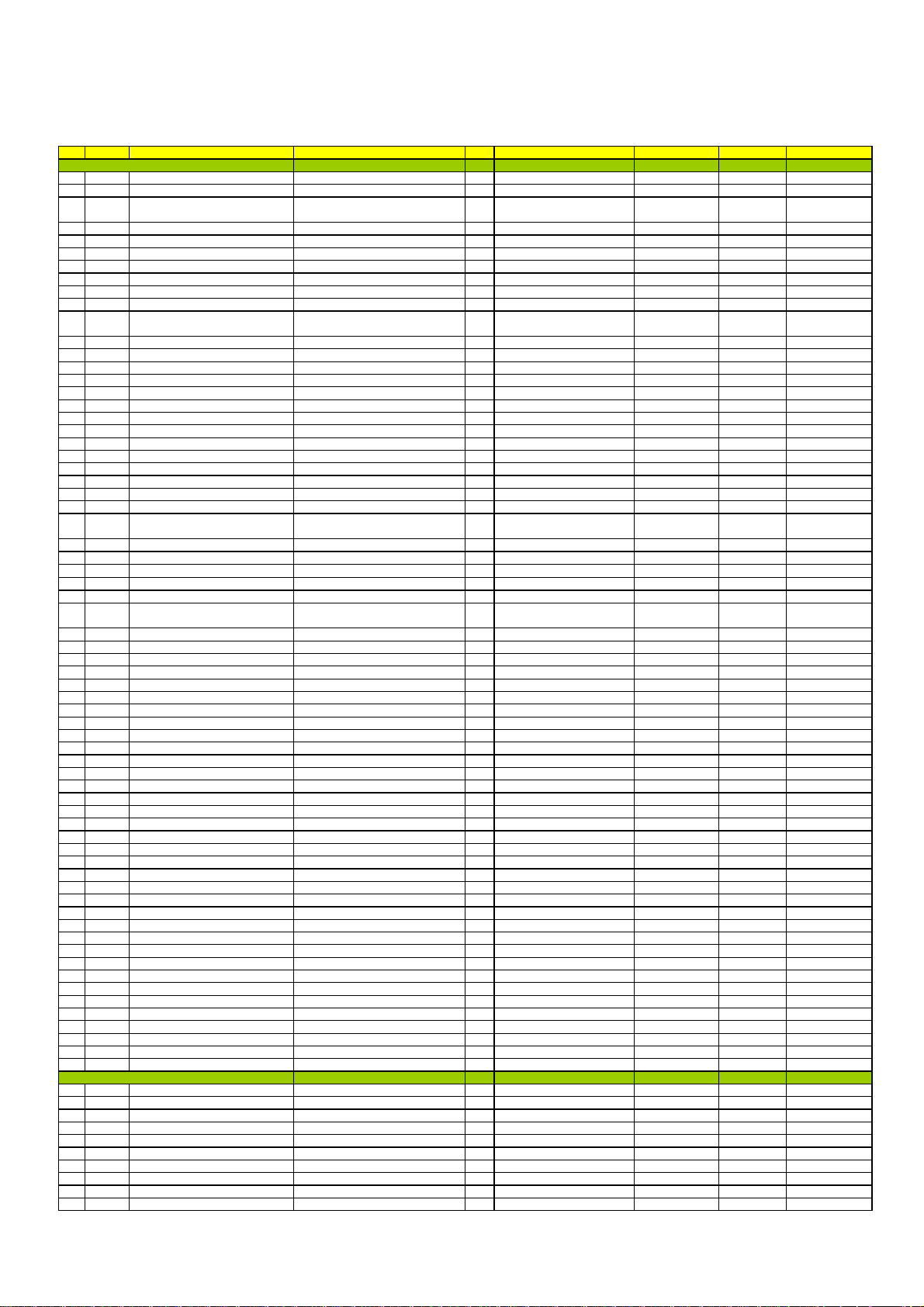
5. PARTS LIST
O
E
MODEL : SP-C500R (RUSSIA)
REPORT DATE : May 8,2003
No. PART N
BASE MAIN SMD ASS'Y (BM_1_3)
1 BASE CPU S3P7528DZZ-QZR8 1 U4 SAMSUNG
2 CAPACITOR,CHIP CERAMIC 100nF,10%,25V,X7R,1608
3 CAPACITOR,CHIP CERAMIC 100nF,+80~-20%,25V,Y5V,1608 9
4 CAPACITOR,CHIP CERAMIC 100pF,5%,50V,NP0,1608 2 C22,C20 SAMSUNG
5 CAPACITOR,CHIP CERAMIC 10nF,10%,50%,X7R,1608 6 C10,C27,C34,C80,C92,C93 SAMSUNG
6 CAPACITOR,CHIP CERAMIC 150pF,5%,50V,NP0,1608 1 C54 SAMSUNG
7 CAPACITOR,CHIP CERAMIC 1nF,10%,50V,X7R,1608 2 C47,C14 SAMSUNG
8 CAPACITOR,CHIP CERAMIC 1.2nF,10%,50V,X7R,1608 1 C48 SAMSUNG
9 CAPACITOR,CHIP CERAMIC 1.5nF,10%,50V,X7R,1608 1 C25 SAMSUNG
10 CAPACITOR,CHIP CERAMIC 1.8nF,10%,50V,X7R,1608 1 C53 SAMSUNG
11 CAPACITOR,CHIP CERAMIC 1uF,+80~-20%,16V,Y5V,1608 7
12 CAPACITOR,CHIP CERAMIC 200pF,5%,50V,NP0,1608 1 C24 SAMSUNG
13 CAPACITOR,CHIP CERAMIC 220nF,10%,50V,X7R,1608 1 C11 SAMSUNG
14 CAPACITOR,CHIP CERAMIC 220pF,5%,50V,NP0,1608 2 C49,C15 SAMSUNG
15 CAPACITOR,CHIP CERAMIC 22nF,10%,50V,X7R,1608 1 C62 SAMSUNG
16 CAPACITOR,CHIP CERAMIC 27pF,5%,50V,NP0,1608 2 C68,C69 SAMSUNG
17 CAPACITOR,CHIP CERAMIC 33nF,10%,50V,X7R,1608 4 C37,C38,C39,C44 SAMSUNG
18 CAPACITOR,CHIP CERAMIC 470pF,5%,50V,NP0,1608 1 C41 SAMSUNG
19 CAPACITOR,CHIP CERAMIC 4.7nF,10%,50V,X7R,1608 2 C52,C26 SAMSUNG
20 CAPACITOR,CHIP CERAMIC 68nF,10%,50V,X7R,1608 1 C50 SAMSUNG
21 DIODE,SWITCHING LS4148 1 D1 VISHAY
22 IC,COMPANDOR SL5015 1 U10 AUK
23 IC,EEPROM CAT24WC02J 1 U6 CATALYST ATMEL AT24C02
24 IC,OP AMP S324 1 U8 AUK
25 IC,SPEECH NETWORK SL5021 1 U1 AUK PHILIPS TEA1062T
26 NA 8
27 PCB PCB-BASE(RUSSIA) 1 PCB1 SUNGWON
28 RESISTOR,VARIABLE EVN5ESX50B14 2 RV3,RV1 PANASONIC
29 RESISTOR-CHIP 0ohm,5%,1/16W,DA,TP,1608 2 R20,C46 SAMSUNG
30 RESISTOR-CHIP 1.5Kohm,5%,1/16W,DA,TP,1608 1 R71 SAMSUNG
31 RESISTOR-CHIP 100Kohm,5%,1/16W,DA,TP,1608 2 R55,R57 SAMSUNG
32 RESISTOR-CHIP 10Kohm,5%,1/16W,DA,TP,1608 9
33 RESISTOR-CHIP 120Kohm,5%,1/16W,DA,TP,1608 1 R13 SAMSUNG
34 RESISTOR-CHIP 12Kohm,5%,1/16W,DA,TP,1608 1 R31 SAMSUNG
35 RESISTOR-CHIP 150Kohm,5%,1/16W,DA,TP,1608 1 R27 SAMSUNG
36 RESISTOR-CHIP 150ohm,5%,1/16W,DA,TP,1608 1 R15 SAMSUNG
37 RESISTOR-CHIP 18Kohm,5%,1/16W,DA,TP,1608 2 R53,R56 SAMSUNG
38 RESISTOR-CHIP 1Mohm,5%,1/16W,DA,TP,1608 1 R648 SAMSUNG
39 RESISTOR-CHIP 2.2Kohm,5%,1/16W,DA,TP,1608 1 R14 SAMSUNG
40 RESISTOR-CHIP 2.4Kohm,5%,1/16W,DA,TP,1608 1 R78 SAMSUNG
41 RESISTOR-CHIP 220Kohm,5%,1/16W,DA,TP,1608 1 R60 SAMSUNG
42 RESISTOR-CHIP 220ohm,5%,1/16W,DA,TP,1608 2 R10,R11 SAMSUNG
43 RESISTOR-CHIP 22Kohm,5%,1/16W,DA,TP,1608 2 R645,R4 SAMSUNG
44 RESISTOR-CHIP 24Kohm,5%,1/16W,DA,TP,1608 1 R54 SAMSUNG
45 RESISTOR-CHIP 27Kohm,5%,1/16W,DA,TP,1608 2 R79,R99 SAMSUNG
46 RESISTOR-CHIP 2.7Kohm,5%,1/16W,DA,TP,1608 2 R103,R8 SAMSUNG
47 RESISTOR-CHIP 3.3Kohm,5%,1/16W,DA,TP,1608 4 R19,R26,R59,R646 SAMSUNG
48 RESISTOR-CHIP 3.9Kohm,5%,1/16W,DA,TP,1608 1 R69 SAMSUNG
49 RESISTOR-CHIP 33Kohm,5%,1/16W,DA,TP,1608 2 R67,R74 SAMSUNG
50 RESISTOR-CHIP 390ohm,5%,1/16W,DA,TP,1608 1 R16 SAMSUNG
51 RESISTOR-CHIP 39Kohm,5%,1/16W,DA,TP,1608 6 R64,R65,R66,R72,R73,R91 SAMSUNG
52 RESISTOR-CHIP 39ohm,5%,1/16W,DA,TP,1608 2 R22,R23 SAMSUNG
53 RESISTOR-CHIP 4.7Kohm,5%,1/16W,DA,TP,1608 1 R33 SAMSUNG
54 RESISTOR-CHIP 470Kohm,5%,1/16W,DA,TP,1608 1 R7 SAMSUNG
55 RESISTOR-CHIP 47Kohm,5%,1/16W,DA,TP,1608 3 R24,R52,R58 SAMSUNG
56 RESISTOR-CHIP 5.6Kohm,5%,1/16W,DA,TP,1608 1 R70 SAMSUNG
57 RESISTOR-CHIP 51Kohm,5%,1/16W,DA,TP,1608 2 R81,R18 SAMSUNG
58 RESISTOR-CHIP 560ohm,5%,1/16W,DA,TP,1608 4 R17,R97,R628,R629 SAMSUNG
59 RESISTOR-CHIP 6.8ohm,5%,1/10W,DA,TP,2012 1 R104 SAMSUNG
60 RESISTOR-CHIP 680ohm,5%,1/16W,DA,TP,1608 1 R102 SAMSUNG
61 RESISTOR-CHIP 910ohm,5%,1/16W,DA,TP,1608 1 R34 SAMSUNG
62 TRANSISTOR KRC405 2 Q13,Q14 KEC
63 TRANSISTOR KTA2015Y 3 Q10,Q11,Q12 KEC
64 TRANSISTOR KTC3876Y 1 Q5 KEC
65 TRANSISTOR KTC4075Y 1 Q15 KEC
66 TRANSISTOR MMBTA42 1 Q4 KEC
BASE MAIN INSERT ASS'Y (BM_1_2)
1 ADAPTOR KG3B-9-300+9-150DU ADAPTOR KINGS
2 CAPACITOR,ELECTROLYTIC 100U/16V(E) 2 C76,C19 SAMYOUNG SAMSUNG
3 CAPACITOR,ELECTROLYTIC 10U/16V(E) 1 C23 SAMYOUNG SAMSUNG
4 CAPACITOR,ELECTROLYTIC 220U/16V(E) 1 C78 SAMYOUNG SAMSUNG
5 CAPACITOR,ELECTROLYTIC 470U/25V(E) 1 C79 SAMYOUNG SAMSUNG
6 CAPACITOR-METAL 470nF,250V,10% 1 C1
7 CAPACITOR-POLYESTER 1nF,250V,10% 2 C6,C5
8 CRYSTAL-UNIT 3.579545/HC-49S 1 X1 K-WELL
9 DIODE,RECTIFIER 1N4004,400V1A,DO-41,TP 5 D2,D3,D4,D5,D8 VISHAY
10 DIODE,ZENER 1N4741A,11V 1 DZ3 VISHAY
DESCRIPTION
SPECIFICATION
QT'Y
1
REFERENC
C13 SAMSUNG
C9,C35,C58,C60,C61,
C67,C77,C91
C36,C40,C45,C51,C57,C59,
C63
R6,C12,C18,
C21,R63,R68,R80,R100,
R9,R12,R30,R32,R61,R62,
R90,R101,R647
1'st VENDOR 2'nd VENDOR REMARK
SAMSUNG
SAMSUNG
SAMSUNG
sp-c500r_parts_list_030508_mp2.xls 1/4 SP-C500R_030506
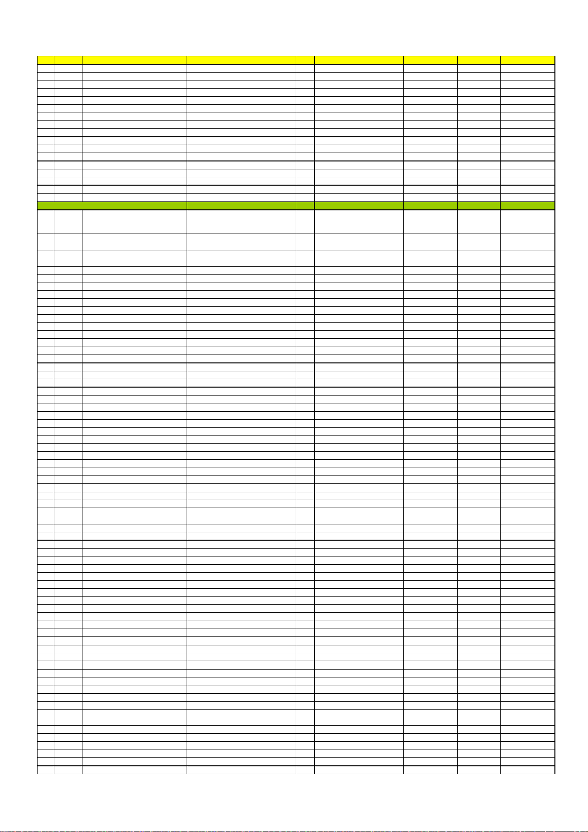
No. PART N
O
E
11 IC,PHOTO COUPLER TCET1103 2 U2,U11 VISHAY
12 IC,REGULATOR KIA7805P 1 U9 KEC
13 INDUCTOR-AXIAL 27uH,10% 2 L4,L5 SANHA
14 INDUCTOR-RADIAL 4mH,10% 2 L2,L3 SANHA
15 JACK-MODULAR AR-623PC-2 1 JP1 ARIN
16 JACK-MODULAR AR-623PC-DEC-4 1 JP3 ARIN
17 JUMPER WIRE 0R(WIRE) 2 DZ2,DZ1
18 LED
19 LED SR3511 1 LD5 AUK
20 LED SM3511 1 LD2 AUK
21 RESISTOR,AXIAL 15K,5%, (1/4W Axial) 2 R2,R1 HANBU
22 RESISTOR,AXIAL 20K,5%, (1/4W Axial) 1 R3 HANBU
23 RESISTOR,AXIAL 33R(1/2W Axial) 1 R105 HANBU
24 SWITCH,TACT
25 TRANSISTOR KTA1277Y 1 Q3 KEC
26 VARISTOR INR7D331K 1 SG1 ILJIN
BASE RF SMD ASS'Y (BRF_1_2)
1 CAPACITOR,CHIP CERAMIC 100nF,10%,25V,X7R,1608 11
2 CAPACITOR,CHIP CERAMIC 100pF,5%,50V,NP0,1608 6
3 CAPACITOR,CHIP CERAMIC 10nF,10%,50V,X7R,1608 5 C301,C319,C338,C353,C357 SAMSUNG
4 CAPACITOR,CHIP CERAMIC 18pF,5%,50V,NP0,1608 1 C390 SAMSUNG
5 CAPACITOR,CHIP CERAMIC 1nF,10%,50V,X7R,1608 4 C309,C326,C388,C398 SAMSUNG
6 CAPACITOR,CHIP CERAMIC 1pF,5%,50V,NP0,1608 4 C345,C363,C367,C395 SAMSUNG
7 CAPACITOR,CHIP CERAMIC 1uF,+80~-20%,25V,Y5V,1608 2 C352,C349 SAMSUNG
8 CAPACITOR,CHIP CERAMIC 220pF,5%,50V,NP0,1608 2 C307,C306 SAMSUNG
9 CAPACITOR,CHIP CERAMIC 22nF,10%,50V,X7R,1608 1 C354 SAMSUNG
10 CAPACITOR,CHIP CERAMIC 27pF,5%,50V,NP0,1608 1 C304 SAMSUNG
11 CAPACITOR,CHIP CERAMIC 2pF,5%,50V,NP0,1608 3 C368,C374,C376 SAMSUNG
12 CAPACITOR,CHIP CERAMIC 33pF,5%,50V,NP0,1608 1 C335 SAMSUNG
13 CAPACITOR,CHIP CERAMIC 39pF,5%,50V,NP0,1608 2 C333,C389 SAMSUNG
14 CAPACITOR,CHIP CERAMIC 3pF,5%,50V,NP0,1608 5 C331,C341,C358,C360,C364 SAMSUNG
15 CAPACITOR,CHIP CERAMIC 47pF,5%,50V,NP0,1608 2 C314,C305 SAMSUNG
16 CAPACITOR,CHIP CERAMIC 4.7nF,10%,50V,X7R,1608 2 C355,C336 SAMSUNG
17 CAPACITOR,CHIP CERAMIC 4pF,5%,50V,NP0,1608 5 C323,C339,C342,C344,C350 SAMSUNG
18 CAPACITOR,CHIP CERAMIC 5.6nF,10%,50V,X7R,1608 1 C302 SAMSUNG
19 CAPACITOR,CHIP CERAMIC 5pF,5%,50V,NP0,1608 4 C372,C393,C394,C399 SAMSUNG
20 CAPACITOR,CHIP CERAMIC 68pF,5%,50V,NP0,1608 1 C334 SAMSUNG
21 CAPACITOR,CHIP CERAMIC 6pF,5%,50V,NP0,1608 2 C359,C361 SAMSUNG
22 CAPACITOR,CHIP CERAMIC 8pF,5%,50V,NP0,1608 3 C340,C343,C362 SAMSUNG
23 CAPACITOR,TANTAL 10U/10V(T) 1 C315 FUJITSU,NEC
24 CAPACITOR-TRIMMER 10pF / ECRJA010A11X 1 CV301 PANASONIC
25 DI-ELECTRIC FILTER DCF2R0814G01 1 F307 EMKO
26 DIODE-ARRAY KDS226 1 D301 KEC
27 DIODE-VVC KDV153 2 D303,D302 KEC
28 DUPLEXER-SAW NSVS631 1 DU301 JRC
29 IC-IF TA31136FN 1 U301 TOSHIBA
30 IC-PLL TB31202FN 1 U302 TOSHIBA
31 INDUCTOR-CHIP CIL21J1R0KNE 1 L303 SAMSUNG
32 RESISTOR-CHIP 0ohm,5%,1/16W,DA,TP,1608 1 C356 SAMSUNG
33 RESISTOR-CHIP 1.2Kohm,5%,1/16W,DA,TP,1608 1 R301 SAMSUNG
34 RESISTOR-CHIP 1.5Kohm,5%,1/16W,DA,TP,1608 1 R337 SAMSUNG
35 RESISTOR-CHIP 100ohm,5%,1/16W,DA,TP,1608 9
36 RESISTOR-CHIP 10Kohm,5%,1/16W,DA,TP,1608 4 R322,R324,R334,R343 SAMSUNG
37 RESISTOR-CHIP 12Kohm,5%,1/16W,DA,TP,1608 1 R332 SAMSUNG
38 RESISTOR-CHIP 150Kohm,5%,1/16W,DA,TP,1608 2 R303,R305 SAMSUNG
39 RESISTOR-CHIP 150ohm,5%,1/16W,DA,TP,1608 1 R387 SAMSUNG
40 RESISTOR-CHIP 180ohm,5%,1/16W,DA,TP,1608 1 R342 SAMSUNG
41 RESISTOR-CHIP 1Kohm,5%,1/16W,DA,TP,1608 1 R389 SAMSUNG
42 RESISTOR-CHIP 2.2Kohm,5%,1/16W,DA,TP,1608 4 R331,R340,R385,R388 SAMSUNG
43 RESISTOR-CHIP 20Kohm,5%,1/16W,DA,TP,1608 1 R302 SAMSUNG
44 RESISTOR-CHIP 22Kohm,5%,1/16W,DA,TP,1608 1 R351 SAMSUNG
45 RESISTOR-CHIP 24Kohm,5%,1/16W,DA,TP,1608 1 R349 SAMSUNG
46 RESISTOR-CHIP 3.3Kohm,5%,1/16W,DA,TP,1608 1 R304 SAMSUNG
47 RESISTOR-CHIP 3.9Kohm,5%,1/16W,DA,TP,1608 3 R326,R327,R328 SAMSUNG
48 RESISTOR-CHIP 33ohm,5%,1/16W,DA,TP,1608 1 R345 SAMSUNG
49 RESISTOR-CHIP 39Kohm,5%,1/16W,DA,TP,1608 1 R347 SAMSUNG
50 RESISTOR-CHIP 4.7Kohm,5%,1/16W,DA,TP,1608 1 R325 SAMSUNG
51 RESISTOR-CHIP 470ohm,5%,1/16W,DA,TP,1608 1 R319 SAMSUNG
52 RESISTOR-CHIP 47Kohm,5%,1/16W,DA,TP,1608 3 R329,R333,R384 SAMSUNG
53 RESISTOR-CHIP 47ohm,5%,1/16W,DA,TP,1608 1 R348 SAMSUNG
54 RESISTOR-CHIP 5.6Kohm,5%,1/16W,DA,TP,1608 2 R330,R339 SAMSUNG
55 RESISTOR-CHIP 51Kohm,5%,1/16W,DA,TP,1608 1 R341 SAMSUNG
56 RESISTOR-CHIP 56Kohm,5%,1/16W,DA,TP,1608 2 R398,R386 SAMSUNG
57 RESISTOR-CHIP 68Kohm,5%,1/16W,DA,TP,1608 1 R338 SAMSUNG
58 RESISTOR-CHIP 8.2Kohm,5%,1/16W,DA,TP,1608 2 R395,R344 SAMSUNG
59 TRANSISTOR BFQ67W 6
60 TRANSISTOR KTN2907AU 1 Q324 KEC
61 TRANSISTOR STC917UF 2 Q304,Q321 AUK
62 TRANSISTOR-FET 3SK320 1 Q320 TOSHIBA
63 TRIMMER POTENTIOMETER 10kohm / EVN5ESX50B14 1 RV301 PANASONIC
64 TRIMMER POTENTIOMETER 500ohm / EVN5ESX50B52 1 RV201 PANASONIC
65 NA 4 C371,C375,C377,C378
DESCRIPTION
SY3511
ST1230B-1
SPECIFICATION
QT'Y
1 LD4 AUK
1 SW1 SEKYEONG
REFERENC
C303,C308,C310,C332,C337,
C351,C365,C373,C379,C381,
C397
C325,C366,C369,C370,C380,
C386
R314,R315,R316,R323,R335,
R336,R346,R350,R399
Q305,Q306,Q307,Q308,Q309,
Q310
1'st VENDOR 2'nd VENDOR REMARK
SAMSUNG
SAMSUNG
SAMSUNG
VISHAY
sp-c500r_parts_list_030508_mp2.xls 2/4 SP-C500R_030506
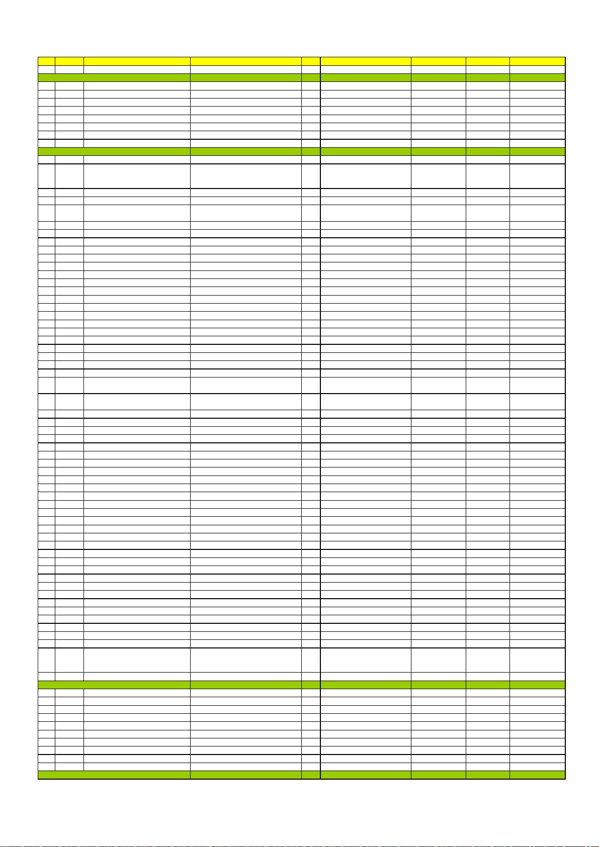
No. PART N
O
E
BASE RF INSERT ASS'Y (BRF_1_2)
1 ANTENNA-WHIP ANTENNA / 90mm 1 ANT1 OSUNG
2 CONNECTOR SYFW200-S02G 1 J301 URI
3 CRYSTAL-FILTER UM-5 / 21.7M15A 1 F302 K-WELL
4 CRYSTAL-UNIT HR-4A / 21.25MHz 1 X301 K-WELL
5 FILTER-CERAMIC LTM450DW 1 F301 CQ
6 INDUCTOR-AIR 0.35*1.6+3.0 2 L301,L302 SANHA
7 INDUCTOR-IFT 5DL-C5001S / 5PLC-K5001Z-KR 1 T301 SANHA TOKO
HANDY MAIN SMD ASS'Y (HM_1_2)
1 CAPACITOR,CHIP CERAMIC 1.8nF,10%,50V,X7R,1608 1 C19 SAMSUNG
2 CAPACITOR,CHIP CERAMIC 100nF,+80~-20%,25V,Y5V,1608 16
3 CAPACITOR,CHIP CERAMIC 100pF,5%,50V,NP0,1608 1 C2 SAMSUNG
4 CAPACITOR,CHIP CERAMIC 1nF,10%,50V,X7R,1608 2 C32,C28 SAMSUNG
5 CAPACITOR,CHIP CERAMIC 1uF,+80~-20%,16V,Y5V,1608 9
6 CAPACITOR,CHIP CERAMIC 2.2nF,10%,50V,X7R,1608 2 C33,C34 SAMSUNG
7 CAPACITOR,CHIP CERAMIC 20pF,5%,50V,NP0,1608 2 C52,C51 SAMSUNG
8 CAPACITOR,CHIP CERAMIC 22nF,10%,50V,X7R,1608 1 C27 SAMSUNG
9 CAPACITOR,CHIP CERAMIC 270pF,5%,50V,NP0,1608 1 C20 SAMSUNG
10 CAPACITOR,CHIP CERAMIC 33nF,10%,50V,X7R,1608 7 C5,C6,C9,C10,C11,C16,C31 SAMSUNG
11 CAPACITOR,CHIP CERAMIC 4.7nF,10%,50V,X7R,1608 1 C18 SAMSUNG
12 CAPACITOR,TANTAL 10U/10V(T) 2 C42,C44 FUJITSU,NEC
13 DIODE,SWITCHING LS4148 2 D1,D2 VISHAY
14 IC-AUDIO AMP NJM2113M 1 U1 JRC
15 IC-COMPANDOR SL5015 1 U2 AUK
16 IC-CONPARATOR S393 1 U4 AUK
17 IC-CPU S3P7235XZZ-QWR5 1 U8 SAMSUNG
18 IC-EEPROM CAT24WC04J 1 U7 CATALYST ATMEL
19 IC-OPAMP S324 1 U3 AUK
20 IC-REGULATOR NJM2871F03 1 U6 JRC
21 IC-VOLTAGE RETECTOR ELM9730NBA 1 U5 ELM
22 PCB PCB-HANDSET(RUSSIA) 1 PCB1 SUNGWON
23 RESISTOR,VARIABLE EVN5ESX50B14 2 RV1,RV2 PANASONIC
24 RESISTOR-CHIP 0ohm,5%,1/16W,DA,TP,1608 5 R11,R21,C35,R50,R58 SAMSUNG
25 RESISTOR-CHIP 100Kohm,5%,1/16W,DA,TP,1608 8
26 RESISTOR-CHIP 10Kohm,5%,1/16W,DA,TP,1608 7
27 RESISTOR-CHIP 15Kohm,5%,1/16W,DA,TP,1608 2 R6,R23 SAMSUNG
28 RESISTOR-CHIP 15ohm,5%,1/16W,DA,TP,1608 1 R65 SAMSUNG
29 RESISTOR-CHIP 18Kohm,5%,1/16W,DA,TP,1608 2 R9,R3 SAMSUNG
30 RESISTOR-CHIP 1Kohm,5%,1/16W,DA,TP,1608 1 R63 SAMSUNG
31 RESISTOR-CHIP 1Mohm,5%,1/16W,DA,TP,1608 2 R26,R55 SAMSUNG
32 RESISTOR-CHIP 2.2Kohm,5%,1/16W,DA,TP,1608 1 R66 SAMSUNG
33 RESISTOR-CHIP 2.7Kohm,1%,1/16W,DA,TP,1608 1 R41 SAMSUNG
34 RESISTOR-CHIP 200ohm,5%,1/16W,DA,TP,1608 1 R57 SAMSUNG
35 RESISTOR-CHIP 220Kohm,5%,1/16W,DA,TP,1608 1 R10 SAMSUNG
36 RESISTOR-CHIP 24Kohm,5%,1/16W,DA,TP,1608 1 R5 SAMSUNG
37 RESISTOR-CHIP 27Kohm,5%,1/16W,DA,TP,1608 4 R29,R30,R31,R32 SAMSUNG
38 RESISTOR-CHIP 2Kohm,1%,1/16W,DA,TP,1608 1 R16 SAMSUNG
39 RESISTOR-CHIP 3.9Kohm,1%,1/16W,DA,TP,1608 1 R37 SAMSUNG
40 RESISTOR-CHIP 3.9Kohm,5%,1/16W,DA,TP,1608 2 R20,R25 SAMSUNG
41 RESISTOR-CHIP 300ohm,1%,1/16W,DA,TP,1608 1 R42 SAMSUNG
42 RESISTOR-CHIP 33Kohm,5%,1/16W,DA,TP,1608 3 R7,R14,R22 SAMSUNG
43 RESISTOR-CHIP 36Kohm,1%,1/16W,DA,TP,1608 1 R38 SAMSUNG
44 RESISTOR-CHIP 39Kohm,1%,1/16W,DA,TP,1608 1 R40 SAMSUNG
45 RESISTOR-CHIP 39Kohm,5%,1/16W,DA,TP,1608 2 R13,R12 SAMSUNG
46 RESISTOR-CHIP 3Kohm,1%,1/16W,DA,TP,1608 1 R34 SAMSUNG
47 RESISTOR-CHIP 47Kohm,1%,1/16W,DA,TP,1608 1 R47 SAMSUNG
48 RESISTOR-CHIP 47Kohm,5%,1/16W,DA,TP,1608 2 R24,R44 SAMSUNG
49 RESISTOR-CHIP 51Kohm,1%,1/16W,DA,TP,1608 2 R35,R36 SAMSUNG
50 RESISTOR-CHIP 56Kohm,5%,1/16W,DA,TP,1608 1 R2 SAMSUNG
51 RESISTOR-CHIP 6.8Kohm,5%,1/16W,DA,TP,1608 1 R19 SAMSUNG
52 RESISTOR-CHIP 62Kohm,1%,1/16W,DA,TP,1608 1 R39 SAMSUNG
53 TRANSISTOR KRA305 4 Q1,Q5,Q6,Q8 KEC
54 TRANSISTOR KRC406 6 Q2,Q3,Q4,Q9,Q11,Q13 KEC
55 TRANSISTOR KTC4075 1 Q7 KEC
56 NA 13
HANDY MAIN INSERT ASS'Y (HM_1_2)
1 AUDIO-RECEIVER SM-28D12 1 SP1 SHINMYUNG
2 BATTERY 3/V350H,3.6V,350mA 1 BT1 VARTA
3 BUZZER MSG1216 1 BZ1 LT COMPONENT
4 CONNECTOR 53014-0210 1 JP1 MOLEX
5 CRYSTAL-UNIT 4.194304/HC-49S 1 X1 K-WELL
6 LCD GD-41010-0-TFPC 1 LCD1 GENDA
7 MIC-CONDENSOR CMP-4542 1 MI1 BSE
8 WIRE 3+120+3mm/#28 BLACK 1 W2
9 WIRE 3+120+3mm/#28 WHITE 1 W1
HANDY RF SMD ASS'Y (HRF_1_2)
DESCRIPTION
SPECIFICATION
QT'Y
REFERENC
C3,C7,C14,C30,C36,C37,
C38,C39,C40,C41,C43,C45,
C46,C50,C53,C54
C1,C4,C8,C12,C17,C21,C24,
C25,C26
R1,R4,R8,R28,R59,R60,R61,
R62
R43,R45,R46,R48,R49,R54,
R64
Q10,C13,R15,R17,R18,
C23,R27,R33,R51,
R52,R53,C55,R56
1'st VENDOR 2'nd VENDOR REMARK
SAMSUNG
SAMSUNG
SAMSUNG
SAMSUNG
sp-c500r_parts_list_030508_mp2.xls 3/4 SP-C500R_030506
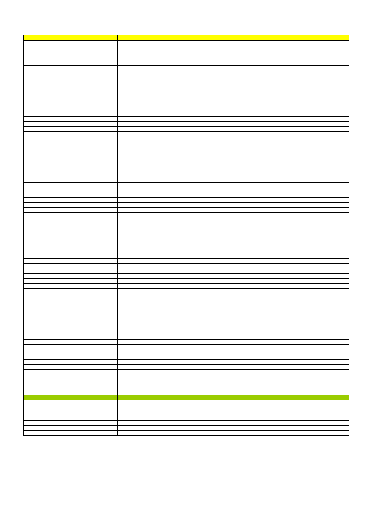
No. PART N
O
E
1 CAPACITOR,CHIP CERAMIC 100nF+80~-20%,25V,Y5v,1608 13
2 CAPACITOR,CHIP CERAMIC 100pF,5%,50V,NP0,1608 4 C325,C366,C369,C386 SAMSUNG
3 CAPACITOR,CHIP CERAMIC 10nF,10%,50V,X7R,1608 4 C319,C338,C353,C357 SAMSUNG
4 CAPACITOR,CHIP CERAMIC 1nF,10%,50V,X7R,1608 5 C309,C326,C376,C388,C398 SAMSUNG
5 CAPACITOR,CHIP CERAMIC 1pF,5%,50V,NP0,1608 5 C327,C345,C363,C367,C377 SAMSUNG
6 CAPACITOR,CHIP CERAMIC 1uF,+80~-20%,25V,Y5V,1608 2 C352,C349 SAMSUNG
7 CAPACITOR,CHIP CERAMIC 220pF,5%,50V,NP0,1608 2 C307,C306 SAMSUNG
8 CAPACITOR,CHIP CERAMIC 27pF,5%,50V,NP0,1608 1 C304 SAMSUNG
9 CAPACITOR,CHIP CERAMIC 2pF,5%,50V,NP0,1608 6
10 CAPACITOR,CHIP CERAMIC 33nF,10%,50V,X7R,1608 1 C301 SAMSUNG
11 CAPACITOR,CHIP CERAMIC 33pF,5%,50V,NP0,1608 1 C335 SAMSUNG
12 CAPACITOR,CHIP CERAMIC 39pF,5%,50V,NP0,1608 1 C333 SAMSUNG
13 CAPACITOR,CHIP CERAMIC 3pF,5%,50V,NP0,1608 4 C339,C368,C374,C393 SAMSUNG
14 CAPACITOR,CHIP CERAMIC 4.7nF,10%,50V,X7R,1608 2 C355,C336 SAMSUNG
15 CAPACITOR,CHIP CERAMIC 47nF,10%,50V,X7R,1608 1 C354 SAMSUNG
16 CAPACITOR,CHIP CERAMIC 47pF,5%,50V,NP0,1608 3 C305,C314,C389 SAMSUNG
17 CAPACITOR,CHIP CERAMIC 4pF,5%,50V,NP0,1608 5 C323,C344,C350,C358,C372 SAMSUNG
18 CAPACITOR,CHIP CERAMIC 5.6nF,10%,50V,X7R,1608 1 C302 SAMSUNG
19 CAPACITOR,CHIP CERAMIC 5pF,5%,50V,NP0,1608 3 C340,C390,C399 SAMSUNG
20 CAPACITOR,CHIP CERAMIC 68pF,5%,50V,NP0,1608 1 C334 SAMSUNG
21 CAPACITOR,CHIP CERAMIC 6pF,5%,50V,NP0,1608 2 C361,C342 SAMSUNG
22 CAPACITOR,CHIP CERAMIC 8pF,5%,50V,NP0,1608 2 C362,C359 SAMSUNG
23 CAPACITOR,CHIP CERAMIC 9pF,5%,50V,NP0,1608 1 C343 SAMSUNG
24 CAPACITOR,TANTAL 10U/10V(T) 1 C315 FUJITSU,NEC
25 CAPACITOR-TRIMMER 10pF /ECRJA010A11X 1 CV301 PANASONIC
26 DI-ELECTRIC FILTER DCF2R0904G01 1 F307 EMKO
27 DIODE-ARRAY KDS226 1 D301 KEC
28 DIODE-VVC KDV153 2 D303,D302 KEC
29 DUPLEXER-SAW NSVS630 1 DU301 JRC
30 IC-IF TA31136FN 1 U301 TOSHIBA
31 IC-PLL TB31202FN 1 U302 TOSHIBA
32 INDUCTOR-CHIP CIL21J1R0KNE 1 L303 SAMSUNG
33 RESISTOR-CHIP 0ohm,5%,1/16W,DA,TP,1608 2 C356,R323 SAMSUNG
34 RESISTOR-CHIP 1.2Kohm,5%,1/16W,DA,TP,1608 1 R301 SAMSUNG
35 RESISTOR-CHIP 100ohm,5%,1/16W,DA,TP,1608 7
36 RESISTOR-CHIP 10Kohm,5%,1/16W,DA,TP,1608 4 R322,R334,R343,R344 SAMSUNG
37 RESISTOR-CHIP 12Kohm,5%,1/16W,DA,TP,1608 3 R332,R351,R398 SAMSUNG
38 RESISTOR-CHIP 150Kohm,5%,1/16W,DA,TP,1608 2 R305,R303 SAMSUNG
39 RESISTOR-CHIP 150ohm,5%,1/16W,DA,TP,1608 2 R342,R387 SAMSUNG
40 RESISTOR-CHIP 1Kohm,5%,1/16W,DA,TP,1608 1 R337 SAMSUNG
41 RESISTOR-CHIP 2.2Kohm,5%,1/16W,DA,TP,1608 4 C313,R331,R383,R385 SAMSUNG
42 RESISTOR-CHIP 20Kohm,5%,1/16W,DA,TP,1608 1 R302 SAMSUNG
43 RESISTOR-CHIP 220ohm,5%,1/16W,DA,TP,1608 1 R399 SAMSUNG
44 RESISTOR-CHIP 22Kohm,5%,1/16W,DA,TP,1608 1 R349 SAMSUNG
45 RESISTOR-CHIP 3.3Kohm,5%,1/16W,DA,TP,1608 2 R340,R304 SAMSUNG
46 RESISTOR-CHIP 3.9Kohm,5%,1/16W,DA,TP,1608 3 R326,R327,R328 SAMSUNG
47 RESISTOR-CHIP 33Kohm,5%,1/16W,DA,TP,1608 1 R347 SAMSUNG
48 RESISTOR-CHIP 33ohm,5%,1/16W,DA,TP,1608 2 R345,R335 SAMSUNG
49 RESISTOR-CHIP 4.7Kohm,5%,1/16W,DA,TP,1608 2 R324,R325 SAMSUNG
50 RESISTOR-CHIP 470ohm,5%,1/16W,DA,TP,1608 1 R319 SAMSUNG
51 RESISTOR-CHIP 47Kohm,5%,1/16W,DA,TP,1608 3 R333,R382,R384 SAMSUNG
52 RESISTOR-CHIP 5.6Kohm,5%,1/16W,DA,TP,1608 2 R330,R339 SAMSUNG
53 RESISTOR-CHIP 51Kohm,5%,1/16W,DA,TP,1608 1 R341 SAMSUNG
54 RESISTOR-CHIP 56Kohm,5%,1/16W,DA,TP,1608 1 R329 SAMSUNG
55 RESISTOR-CHIP 68Kohm,5%,1/16W,DA,TP,1608 2 R338,R386 SAMSUNG
56 RESISTOR-CHIP 8.2Kohm,5%,1/16W,DA,TP,1608 1 R395 SAMSUNG
57 RESISTOR-CHIP 820ohm,5%,1/16W,DA,TP,1608 1 R389 SAMSUNG
58 TRANSISTOR BFQ67W 6
59 TRANSISTOR KTN2907AU 2 Q323,Q324 KEC
60 TRANSISTOR STC917UF 2 Q304,Q321 AUK
61 TRANSISTOR-FET 3SK320 1 Q320 TOSHIBA
62 TRIMMER POTENTIOMETER 10kohm / EVN5ESX50B14 1 RV301 PANASONIC
63 TRIMMER POTENTIOMETER 500ohm / EVN5ESX50B52 1 RV201 PANASONIC
64 NA 2 C375,C392
HANDY RF INSERT ASS'Y (HRF_1_2)
1 ANTENNA-HELICAL ANTENNA 1 ANT1 MJTEL
2 CONNECTOR SYFW200-S02G 1 J301 URI
3 CRYSTAL-FILTER UM-5 / 21.7M15A 1 F302 K-WELL
4 CRYSTAL-UNIT HR-4A / 21.25MHz 1 X301 K-WELL
5 FILTER-CERAMIC LTM450DW 1 F301 CQ
6 INDUCTOR-AIR 0.35*1.6+3.0 2 L301,L302 SANHA
7 INDUCTOR-IFT 5DL-C5001S / 5PLC-K5001Z-KR 1 T301 SANHA TOKO
DESCRIPTION
SPECIFICATION
QT'Y
REFERENC
C303,C308,C310,C332,C337,
C351,C365,C370,C373,C379,
C380,C381,C397
C331,C341,C360,C364,C371,
C394
R314,R315,R316,R336,R346,
R348,R350
Q305,Q306,Q307,Q308,Q309,
Q310
1'st VENDOR 2'nd VENDOR REMARK
SAMSUNG
SAMSUNG
SAMSUNG
VISHAY
sp-c500r_parts_list_030508_mp2.xls 4/4 SP-C500R_030506
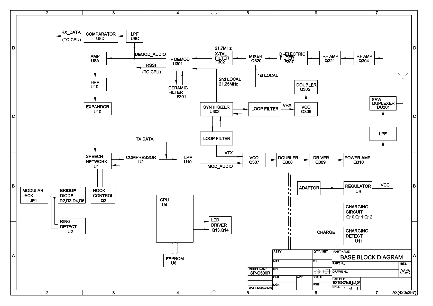
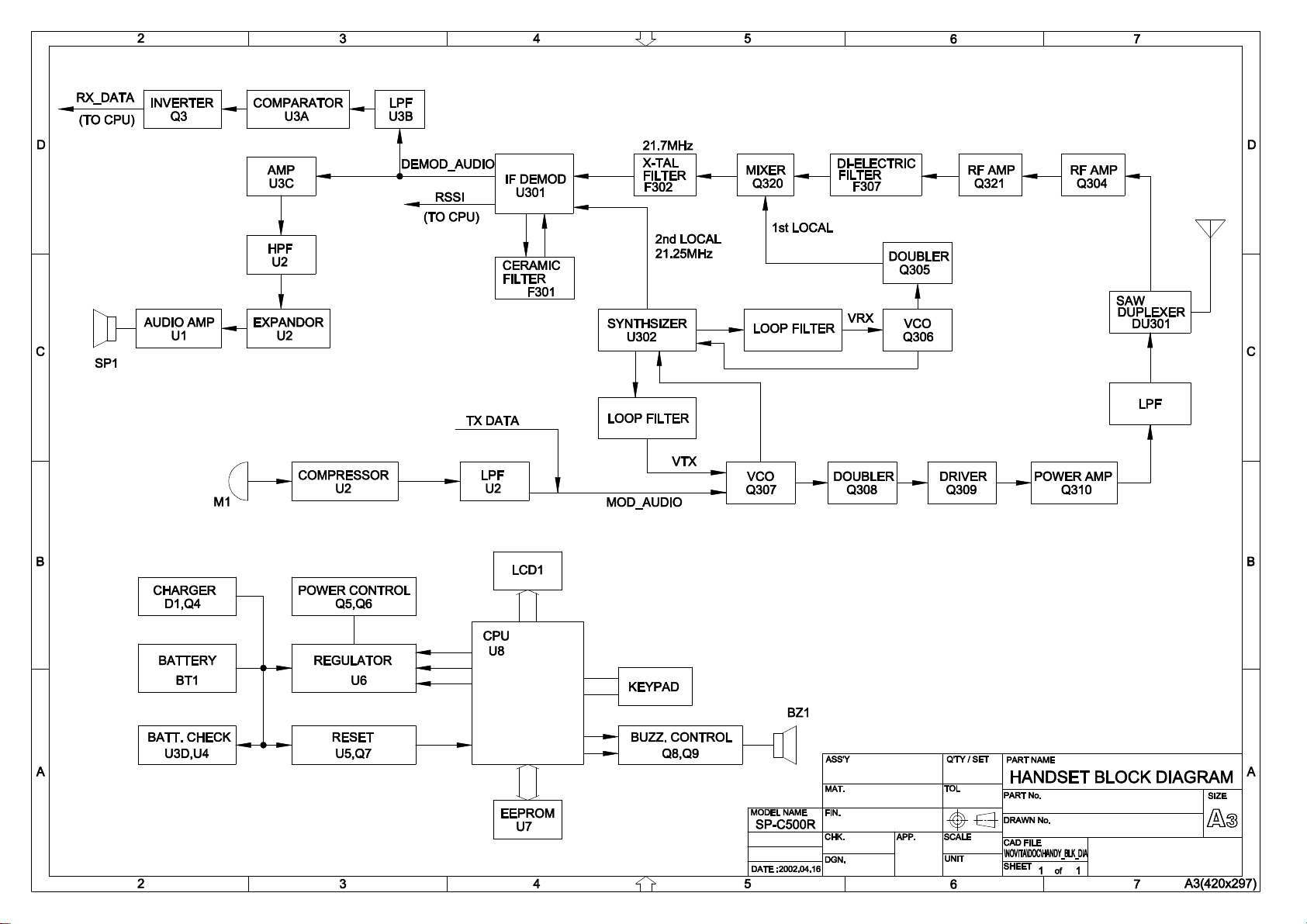
6. Block Diagram
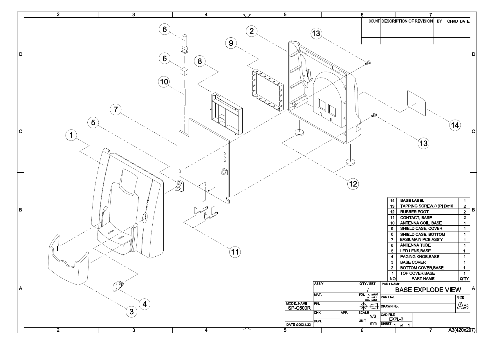
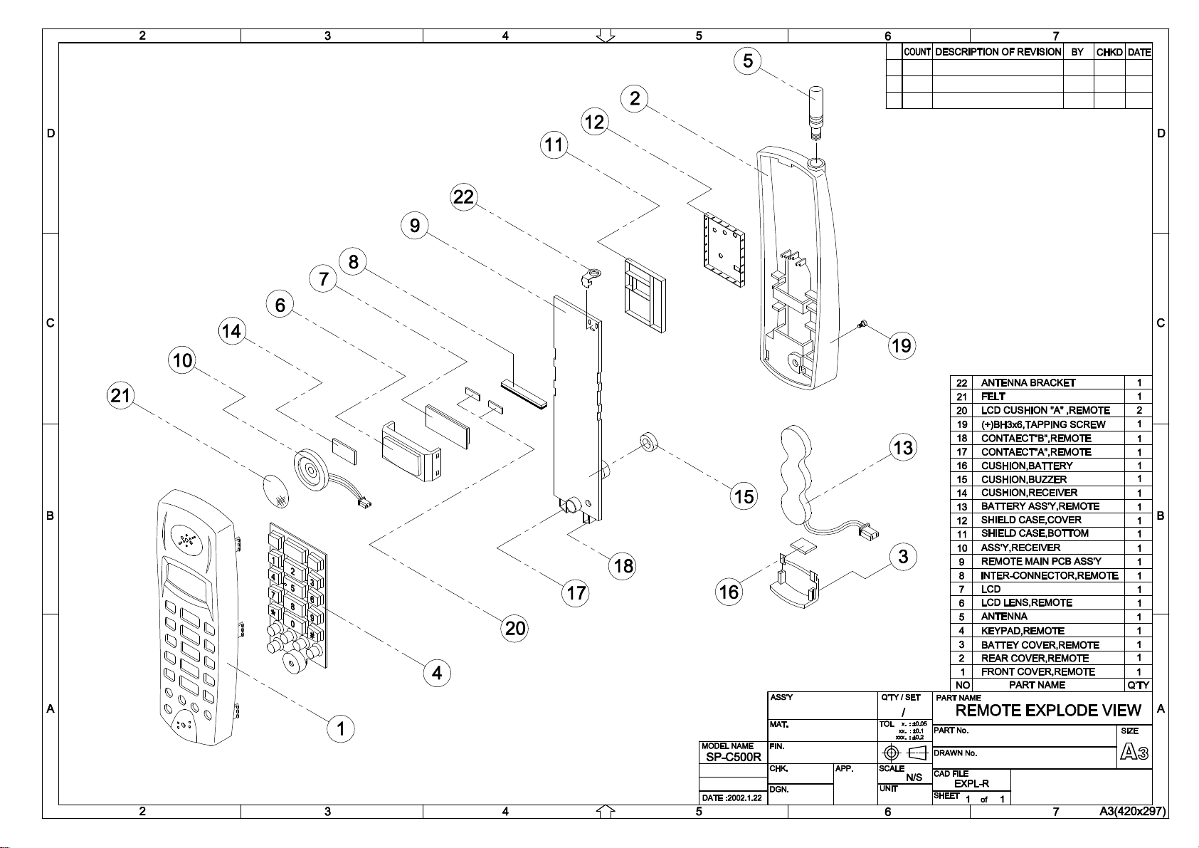
7. Explode View
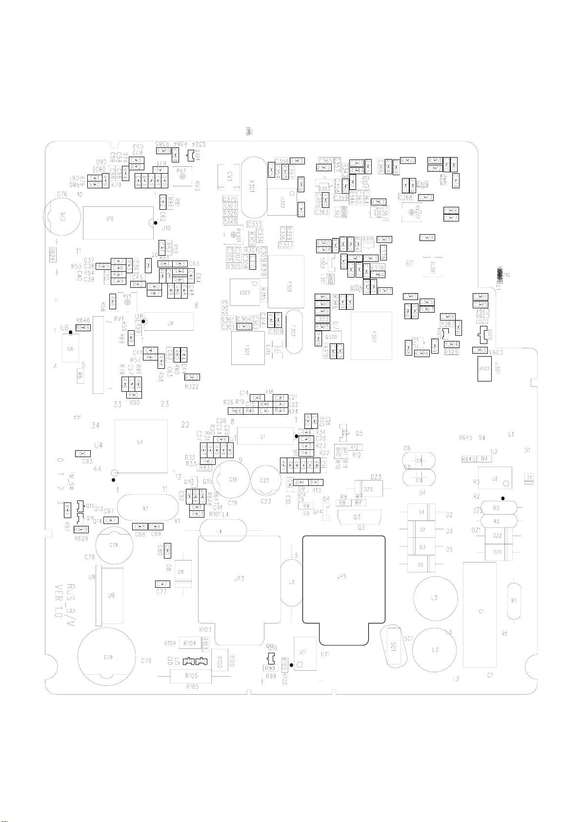
8. Reference Map
8.1 Base Logic Top
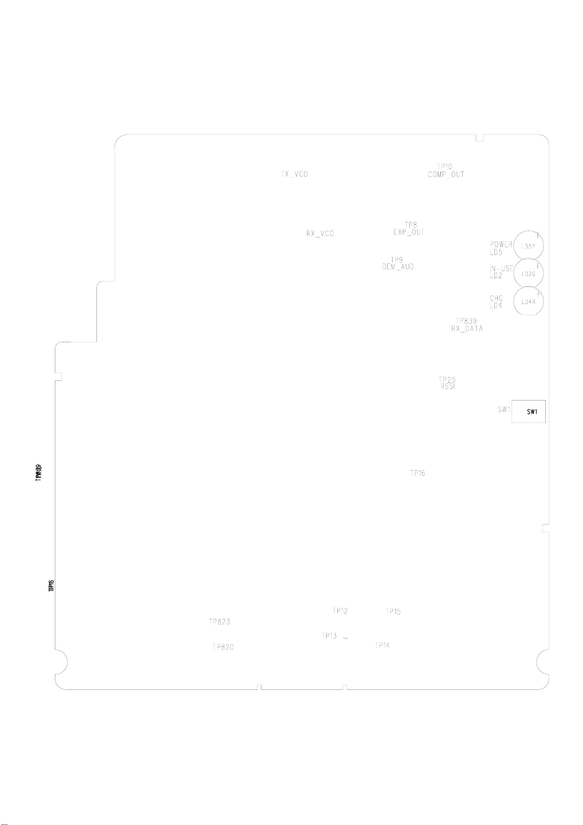
8.2 Base Logic Bottom

8.3 Remote Logic Top
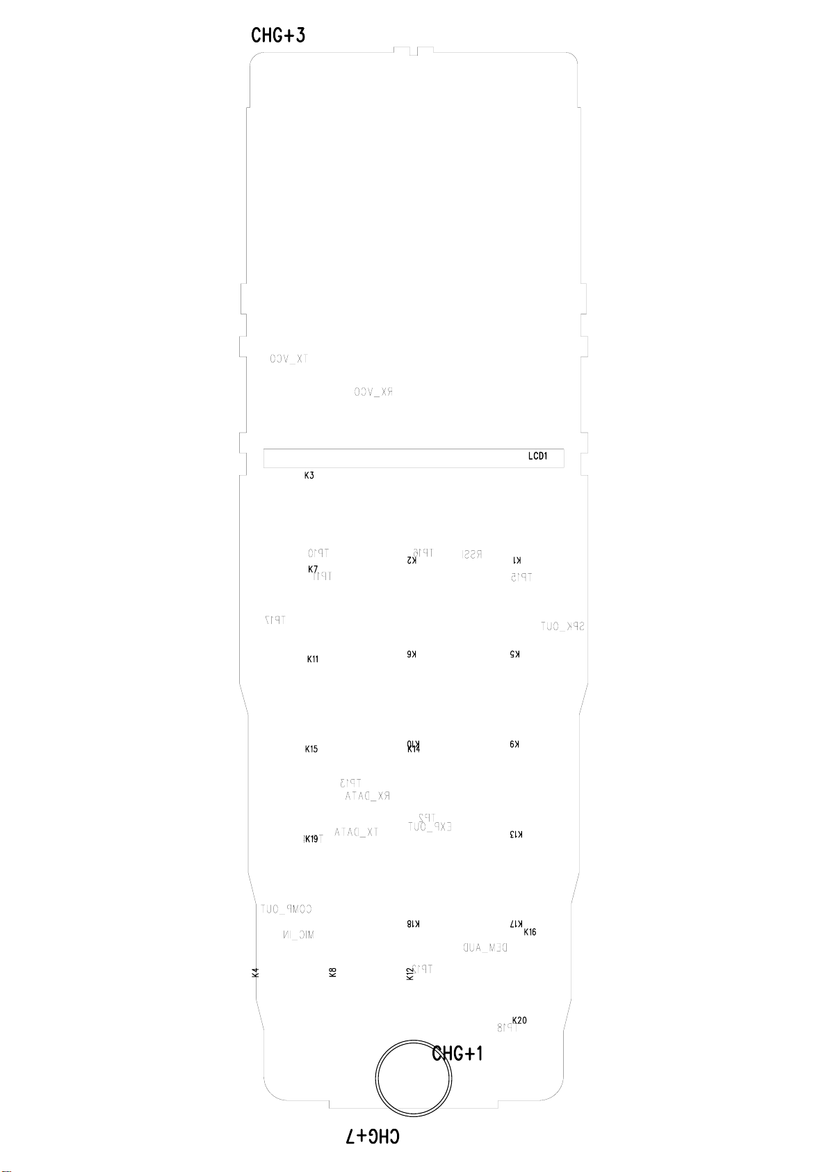
8.4 Remote Logic Bottom

9. CIRCUIT DESCRIPTION
1. Base Unit Section
1.1. Power supply circuit
The DC 9V from the AC adaptor is supplied to JP3 (DC modular jack).
This input voltage is supplied to the main circuit through D8 (diode) and supplied to
the charge circuit.
The voltage from D8 is regulated to 5V by regulator U9. This regulated 5V is supplied
to main circuit and RF circuit.
1.2. Charge circuit
Charging circuit is composed of U11,Q10,Q11,Q12,R99,R100,R102,R103,R104 and
R105.
This charging circuit supplies constant current to the handset batteries through
CHG+1 and CHG-1.
When the charge current flows, U11 (photo-coupler) detects the current and send a
CHARGE signal to pin 41 of U4 (CPU).
Then LD4 is lighted.
1.3. Receiving audio signal from telephone line
The audio signal from JP1 (telephone line modular jack) goes pin 1 of U1 (speech
network) through bridge diode composed of D2, D3, D4 and D5, and switching
transistor Q3.
After being amplified in speech network, it comes out from pin 4 and goes to the pin8
of U10 (compander) through R81 and C62.
This signal is amplified and compressed for noise reduction then goes through 3rd
order low pass filter composed of op amp. in U10, C52, C53, C54 R72, R73 and R74.
This signal is sent to the modulation input (MOD_AUDIO) of the RF block through C51,
R70 and RV3 and transmitted to the handset.
1.4. Sending audio signal to telephone line
Received RF signal from handset is detected in the RF block and the demodulated
audio signal(DEMOD_AUDIO) is filtered by low pass filter composed of U8A, C41, R57,
R58 and R59 through C44. This audio signal is filtered again by high pass filter
composed of op amp in U10, C37, C38, C39, R53, R54 and R55 then expanded in
U10.

The expanded signal coming from pin 19 of U10, and goes to the pin 6 and 7 of
U1 (speech network) through C34 and R52.
Speech network adjusts a transmit signal gain and sends it to the telephone line
through switching transistor Q3, bridge diode (D2, D3, D4 and D5) and modular jack
JP1.
1.5. Sending and Receiving of data signal
The sending data comes out from TX_DATA of CPU (pin 28), and enters into pin 4 of
U10 (compander).
It is modulated at RF block through the same path as audio signal.
The received data which demodulated at RF block with the same manner as audio
signal is going to the low path filter composed of U8C, C47, C48, C49, R64,R65 and
R67. Filtered signal is comparated at U8D. The square wave from U8D(RX_DATA) is
fed to pin 39 of CPU.
1.6. Ring detector circuit
When the ring signal is supplied to U2(photo coupler) through C1, R1, DZ1, DZ2, U2
detects it and send a RING_SIGNAL signal to pin 42 of U4 (CPU).
The base unit send a ringing data through the "sending data path" to the handset.
1.7. DTMF signal
In case that the tone/pulse mode is set tone position, it is possible to use DTMF dial.
DTMF signal is generated by U1 by the command from CPU (Pin 34).
DTMF signal from CPU (pin 34) is supplied to the pin 11 of U1 and sent to the
telephone line.
When DTMF signal is sent to telephone, pin 4, 5, 6, 7 of U1 is muted by CPU (pin
35).
1.8. Pulse dialing
In case that the tone/pulse mode is set pulse position, it is possible to use pulse dial.
The pulse signal is made by switching Q4 (switching TR) on or off (CPU pin 37).
1.9. EEPROM
U6 is the EEPROM.
This stores the identification code which are inherent to pair of base unit and handset
to safe guard against interference.

1.10. Reset circuit
When power is supplied to the base unit, C91 is shorted momentary, and Q15 is turn
on momentary. Then pin 12 of CPU become low a few millisecond, and CPU is reset.
1.11. LED driver circuit
When power is supplied to base unit, LD5 becomes light, and LD2, LD4 become light
on and off.
If handset is cradled at base unit, pin 4 of CPU becomes high and Q14 is turn on,
then LD4 is lighted.
And if base unit is linked with handset, pin 3 of CPU becomes high and Q13 is turn
on, then LD2 (green LED) is lighted.
1.12. Speech network
R20,R34,C18 and C119 are used for impedance matching between telephone line and
phone.
The R15,R16,C11,C12,C13 connected pin10, 16 of U1 are for side tone balance.
2. Base RF Block Section
2.1. RX VCO circuit
RX VCO circuit is configured by Q305, Q306, D302 (varicap diode), L301 (air coil),
and some additional passive parts.
The control voltage from pin 14 (charge pump out) of the U302 (PLL IC) is supplied
to the D302 cathode through passive loop filter (C336, C337, C338, R329, R330,
R331) to control the oscillation frequency.
L301 is used to adjust the oscillation frequency band.
The oscillation frequency of 450MHz band signal goes to pin 16 of U302 via C345.
The oscillator output is doubled by Q305 (doubler) and fed into Q320 (RX mixer).
2.2. TX VCO circuit
TX VCO circuit is configured by Q307, D303, L302 and some additional passive parts.
The control voltage from pin 3 (charge pump out) of the U302 is supplied to the D303
cathode through passive loop filter (C353, C354, C355, R338, R339, R340) to control
the oscillation frequency.
The modulating signal is supplied to D303 anode.
L302 is used to adjust the oscillation frequency band.
The oscillation frequency of 450MHz band signal goes to pin 1 of U302 via C363.
 Loading...