

Samsung sn761678b Service manual
www.ti.com
FEATURES
1
2
3
4
5
6
7
8
9
10
11
12
13
14
15
30
29
28
27
26
25
24
23
22
21
20
19
18
17
16
VHIOSCC
VHIOSCB
OSCGND
VLOOSCC
VLOOSCB
UHFOSCB1
UHFOSCC1
UHFOSCC2
UHFOSCB2
IFGND
VCC
IFOUT
CP
VTU
XTAL
UHFRFIN
VHFRFIN
BS4
RFGND
MIXOUT2
MIXOUT1
IFIN2
IFIN1
BS2
BS1
BS3
ADC
AS
SDA
SCL
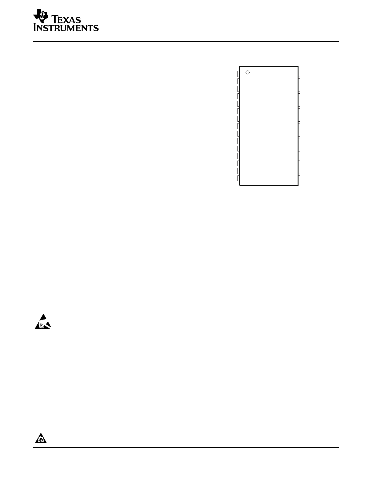
DBTPACKAGE
(TOP VIEW)
P0038-01
• Single-Chip Mixer/Oscillator and
Phase-Locked Loop (PLL) Synthesizer
• Three-Band Local Oscillator
• I2C Bus Protocol (Bidirectional Data
Transmission)
• 30-V Tuning Voltage Output
• Four NPN-Type Band-Switch Drivers
• Programmable Reference Divider Ratio
(512, 640, or 1024)
• External 4-Pin Intermediate Frequency (IF)
Filter Between Mixer Output and IF Amplifier
Input
• 5-V Power Supply
• 30-Pin Thin Shrink Small-Outline Package
(TSSOP)
APPLICATIONS
• TVs
• VCR/DVD Recorders
• Set-Top Boxes
SN761678B
TV TUNER IC
SLES185 – JUNE 2006
DESCRIPTION
The SN761678B is a synthesized tuner IC designed for TV tuning systems. The circuit consists of a
phase-locked loop (PLL) synthesizer, three-band local oscillator and mixer, 30-V output tuning amplifier, and four
NPN band-switch drivers. The device is available in a small-outline package. A 15-bit programmable counter and
reference divider are controlled by I2C bus protocol. Tuning step frequency is selectable by this reference divider
ratio for a crystal oscillator.
blk
blk
blk
blk
blk
blk
PRODUCTION DATA information is current as of publication date.
Products conform to specifications per the terms of the Texas
Instruments standard warranty. Production processing does not
necessarily include testing of all parameters.
This integrated circuit can be damaged by ESD. Texas Instruments recommends that all integrated circuits be handled with
appropriate precautions. Failure to observe proper handling and installation procedures can cause damage.
ESD damage can range from subtle performance degradation to complete device failure. Precision integrated circuits may be
more susceptible to damage because very small parametric changes could cause the device not to meet its published
specifications.
Please be aware that an important notice concerning availability, standard warranty, and use in critical applications of Texas
Instruments semiconductor products and disclaimers thereto appears at the end of this data sheet.
Copyright © 2006, Texas Instruments Incorporated
www.ti.com
B0089-02
IF
Amplifier
Operational
Amplifier
XTAL
Oscillator
4MHz
1/8
Prescaler
512/640/1024
Divider
1/32,1/33
Prescaler
Phase
Detector
15-Bit
Counter
Charge
Pump
I CBus
2
Interface
5-Level
ADC
IFOUT
IFGND
VTU
CP
VHFRFIN
UHFRFIN
RFGND
XTAL
SCL
SDA
AS
NPNBand-SwitchPort
VLOOSCB
VHIOSCC
OSCGND
VLOOSCC
VHIOSCB
UHFOSCB1
UHFOSCC1
UHFOSCC2
UHFOSCB2
MIXOUT1
MIXOUT2
VCC
BS1
ADC
BS2
BS3
BS4
VHF-L
Oscillator
VHF-H
Oscillator
UHF
Oscillator
VHF
Mixer
UHF
Mixer
IFIN2
IFIN1
SN761678B
TV TUNER IC
SLES185 – JUNE 2006
FUNCTIONAL BLOCK DIAGRAM
2
Submit Documentation Feedback
www.ti.com
18
S0159-01
150kW
50kW
19
S0133-03
SN761678B
TV TUNER IC
SLES185 – JUNE 2006
Terminal Functions
TERMINAL
NAME NO.
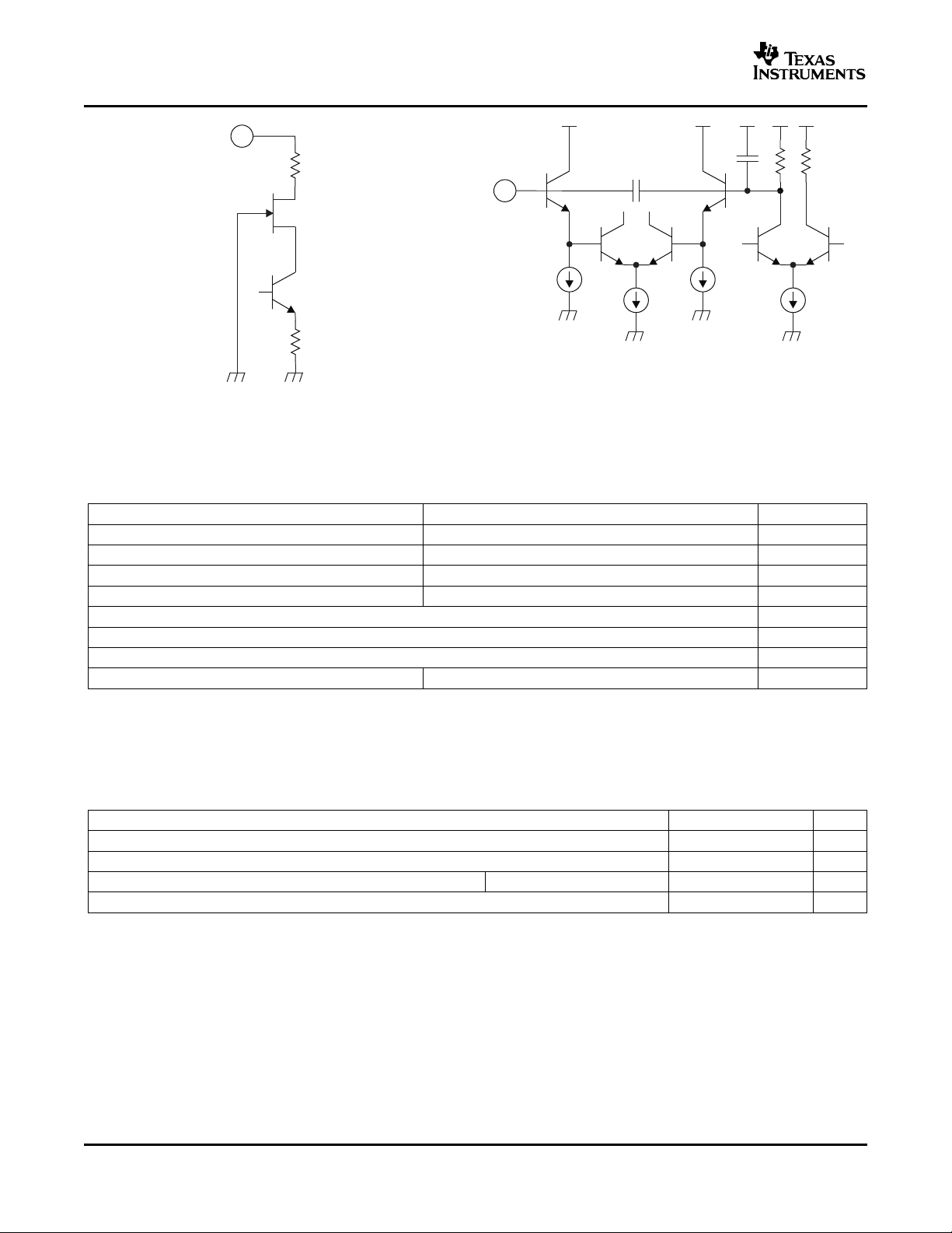
ADC 19 ADC input Figure 1
AS 18 Address selection input Figure 2
BS1 21 Band-switch 1 output (NPN emitter follower) Figure 4
BS2 22 Band-switch 2 output (NPN emitter follower) Figure 4
BS3 20 Band-switch 3 output (NPN emitter follower) Figure 4
BS4 28 Band-switch 4 output (NPN emitter follower) Figure 4
CP 13 Charge-pump output Figure 5
IF GND 10 IF ground
IF IN1 23 IF amplifier input 1 Figure 3
IF IN2 24 IF amplifier input 2 Figure 3
IF OUT 12 IF output Figure 6
MIX OUT1 25 Mixer output 1 Figure 7
MIX OUT2 26 Mixer output 2 Figure 7
OSC GND 3 Oscillator ground
RF GND 27 RF ground
SCL 16 Serial clock input Figure 8
SDA 17 Serial data input/output Figure 9
UHF OSC B1 6 UHF oscillator base 1 Figure 10
UHF OSC B2 9 UHF oscillator base 2 Figure 10
UHF OSC C1 7 UHF oscillator collector 1 Figure 10
UHF OSC C2 8 UHF oscillator collector 2 Figure 10
UHF RF IN 30 UHF RF input Figure 11
VCC 11 Supply voltage for mixer/oscillator/PLL: 5 V
VHF RF IN 29 VHF RF input Figure 12
VHI OSC B 2 VHF HIGH oscillator base Figure 13
VHI OSC C 1 VHF HIGH oscillator collector Figure 13
VLO OSC B 5 VHF LOW oscillator base Figure 14
VLO OSC C 4 VHF LOW oscillator collector Figure 14
VTU 14 Tuning voltage amplifier output Figure 15
XTAL 15 4-MHz crystal oscillator input Figure 16
DESCRIPTION SCHEMATIC
Figure 1. Figure 2.
Submit Documentation Feedback
3
www.ti.com
20p
20p
23
24
22
28
21
20
S0138-02
50kW
12
S0155-01
13
S0156-01
S0160-01
25
26
16
S0136-03
SN761678B
TV TUNER IC
SLES185 – JUNE 2006
Figure 3. Figure 4.
4
Figure 5. Figure 6.
Figure 7. Figure 8.
Submit Documentation Feedback

www.ti.com
17
S0133-02
8
9
7
6
3kW3kW
S0130-01
S0142-05
30
S0142-04
29
S0129-01
3kW3kW
1
2
S0129-02
3kW3kW
4
5
Figure 9. Figure 10.
SN761678B
TV TUNER IC
SLES185 – JUNE 2006
Figure 11. Figure 12.
Figure 13. Figure 14.
5
Submit Documentation Feedback
www.ti.com
S0158-01
15
14
S0157-01
SN761678B
TV TUNER IC
SLES185 – JUNE 2006
Figure 15. Figure 16.
Absolute Maximum Ratings
over operating free-air temperature range (unless otherwise noted)
Supply voltage range, V
Input voltage 1, V
Input voltage 2, V
Input voltage 3, V
GND
VTU
IN
Continuous total dissipation, P
Operating free-air temperature range, T
Storage temperature range, T
Maximum junction temperature, T
Maximum short-circuit time, t
(1) Stresses beyond those listed under "absolute maximum ratings" may cause permanent damage to the device. These are stress ratings
only, and functional operation of the device at these or any other conditions beyond those indicated under "recommended operating
conditions" is not implied. Exposure to absolute-maximum-rated conditions for extended periods may affect device reliability.
(2) Voltage values are with respect to the IF GND of the circuit.
(3) Derating factor is 8.57 mW/ ° C for TA≥ 25 ° C.
(2)
CC
(2)
(2)
(2)
(3)
D
A
stg
J
SC(max)
VCC (pin 11) –0.4 V to 6.5 V
OSC GND, RF GND (pins 3, 27) –0.4 V to 0.4 V
VTU (pin 14) –0.4 V to 35 V
Other pins (1, 2, 4–9, 12, 13, 15–26, 28–30) –0.4 V to 6.5 V
TA≤ 25 ° C 1071 mW
Each pin to V
(1)
or to GND 10 s
CC
–20 ° C to 85 ° C
–65 ° C to 150 ° C
150 ° C
Recommended Operating Conditions
Supply voltage, V
Tuning supply voltage, V
Output current of band switch, I
Operating free-air temperature, T
6
CC
TU
MIN NOM MAX UNIT
4.5 5 5.5 V
30 33 V
BS
A
One port on 10 mA
–20 85 ° C
Submit Documentation Feedback
 Loading...