

Level
8.
Block Diagram
8-1.
Repair
3
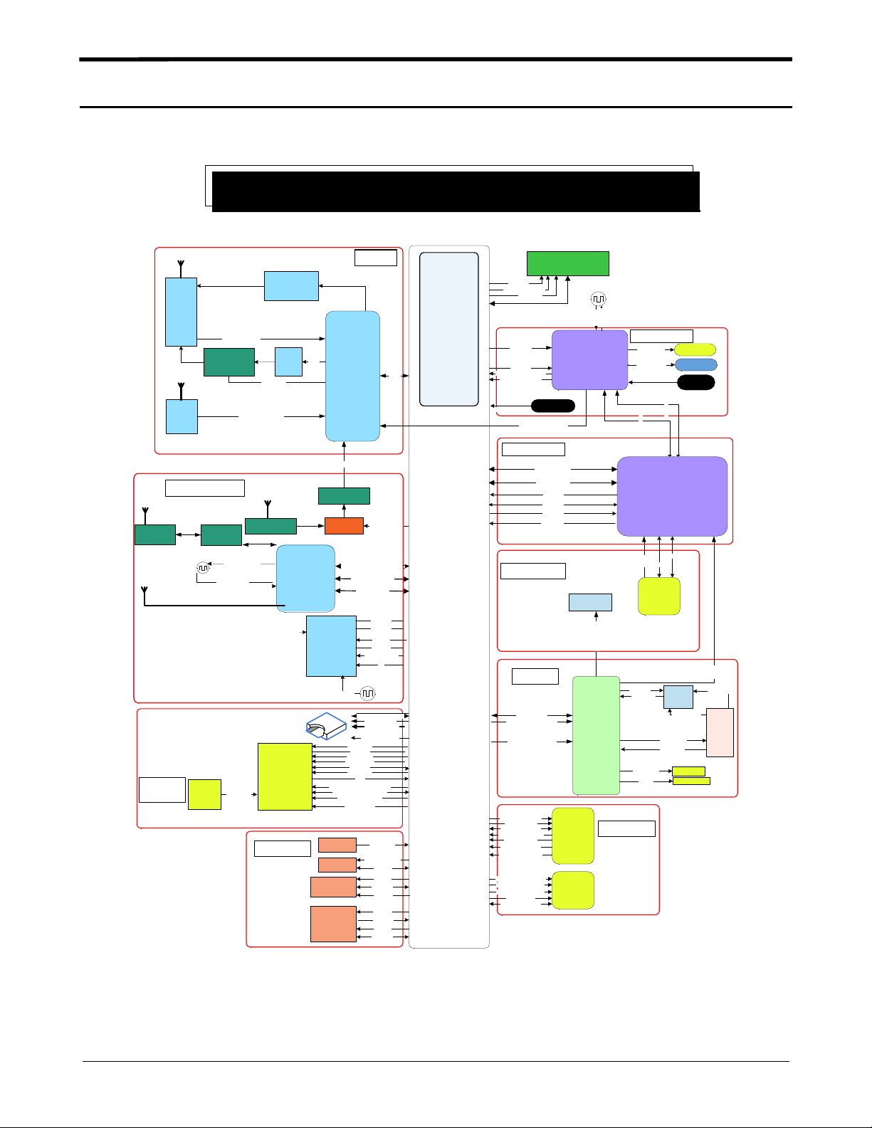
MS01 LTE (SM-G7105) BLOCK DIAGRAM
BT/WIFI
ANT
Diplexer
DPX165950
DT-8126A1
EAR
JACK
ANTENNA )
(
LCD
TSP
Main
ANT
FEMID
LMSW54
GM-G27
Duplexer
SAYEY2G53BA0F0A
Diversity
ANT
DIVER
SITY
FEM
D5099
Connectivity
BPF
ACPF-7024
-SG1
XTAL (FA-128-48 MH z)
BLIC
2G Quad Tx
3G B1,2,5,8 Tx
LTE B1,3,5,8 Tx
2G Quad Rx
3G B1, 2,5,8 Rx
LTE B1,3,5 ,8,20 Rx
BT_WIFI_
CLK(48MHz )_OUT
BT_WIFI _
CLK(48MHz )_IN
LED_A_20V
MMMB PAM
LTE B7 Rx
WB1/WB 5/WB 8/
LB3/ LB7/ LB20
Diversity Rx
SAW
SSFFHHGG8899DDAA000022
NFC Ant
HD TFT LCD
SENSOR
SKY77630
B7
PAM
RF7907
TR7
GPS
ANT
BT/WI-FI/FM
WCN3660 A
NFC_ANT
SD/SIM1
5.25"
&
TSP
LTE
B7 Tx
TRANCEIVER
WTR1625L
GPS_RF_IN
SAW
SSFFHHGG8899YYQQ110022
LNA
MXDLN16S
NFC
S3FNRN3
NFC_CLK
MIPI_DSI 0_CLK_M/P(499 NHz)
MIPI_DSI 0_LANE[0:2]_M /P
MIPI_DSI 0_RESET_N
HALL IC
COMPASS
ACCELATOR
RCV
/PROXY
RF
2G
3G
LTE
GPS
GPS_EXT _CTRL
WLAN(IN, IP,QP,QM,DATA ,CTL)
BT_SSBI_ DATA_CTL
FM_DATA_ SSBI
NFC_SDA
NFC_SCL
NFC_EN
NFC_IRQ
NFC FIRMWARE
I2C
XTAL
(27.1 2 MHz)
T_FLASH_ CLK(50MHz
T_FLASH_ CMD
T_FLASH_ D(0:3)
UIM1_CLK (50MHz)
/RST/DATA
LED_A_20V
LED_K1/2
TS_I2C_SCL
TS_I2C_DATA
TS_INT_N
DSI_RST _N
VGH
LCD_PWM _BL
DETECT_
FLIPCOVER
I2C_SCL (192KHz)
I2C_SDA
I2C_SCL
I2C_DATA
ACC_INT
RCV_P/N
ALSP_INT
I2C_SCL
I2C_DATA
MSM
( CP+ AP )
1.2GHz
)
POP
1.5Gb LPDDR 3
SDRAM
RESET_N
SDC1_CLK (200MHz)
SDC1_CMD
SDC1_D(0:7)
SSBI_MSM
PS_HOLD
BBCLK1(19 .2MHz)_MSM
SLEEP_CLK (32.192)
VOL_UP/ DOWN
RFCLK1_19. 2MHz
MUIC
SUB BRD
AUDIO
SLIMBUS _Data
SLIMBUS_ CLK(28.8MHz )
PMIC_AUDIO _REF_
CLK(19.2MHz)
CAM_MCLK (24MHz)
CAM_RESET _N
CAM_I2C_ SDA/SCL
CAM_CSIO_LANE [0:3]
CAM_CSIO_M /P
CIS_SPI_SCLK /SSN
CIS_SPI_MOSI /MISO
VT_CAM_MCLK (24MHz)
MIPI_CSI1 _DATA0_M/P
MIPI_CSI 1_CLK_M/P_F
CAM2_RST _N
CAM_I2C_ SDA/SCL
eMMC 8GB
KLM 8G1WEMB -B 031
PMIC
PM8926
VVOOLL..KKEEYY
UART_BOOT _ON
USB_HS_ D_M/P
CHG_DET
MUS_SDA
MUS_SCL
MUSB_INT
MMAAIINN MMIICC
AAUUDDIIOO CCOODDEECC
WCD9306
8M CAM
VT CAM
XXTTAALL
((1199..22MMHHzz))
T
N
U
I
_
O
_
M
9
M
1
9
1
MM
//
PP
__
CC
II
MM
__
NN
II
AA
MM
CAMERA
PMIC
MOTOR_ P(N)
VCAM_FLASH
PM_KYPD_PWR_N
NN
__
NN
OO
__
GG
II
JJ
DD
II
__
BB
SS
USB_DP
UU
EAR_ADC
SEND_END
SPK_OUT _N
SPK_OUT _P
RCV_P
RCV_N
MMOOTTOORR
Flash LED
DD
XX
TT
//
DD
XX
RR
__
TT
RR
AA
UU
MMUUIICC
TSU6721 YFPR
USB_DM
IFC
CCOOMMPP..
EAR_DET _3.5
EARSPK_ R/L
EAR_MIC_M /P
SSPPEEAAKKEERR
RREECCEEIIVVEERR
PPOOWWEERR
KKEEYY
RR
//
LL
__
SS
PP
VV
EAR_DET_ 3.5
33..55ppii
EEAARR
JJAACCKK
8-1
Confidential and proprietary-the contents in this service guide subject to change without prior notice.
Distribution, transmission, or infringement of any content or data from this document without Samsung’swritten authorization is strictly prohibited.
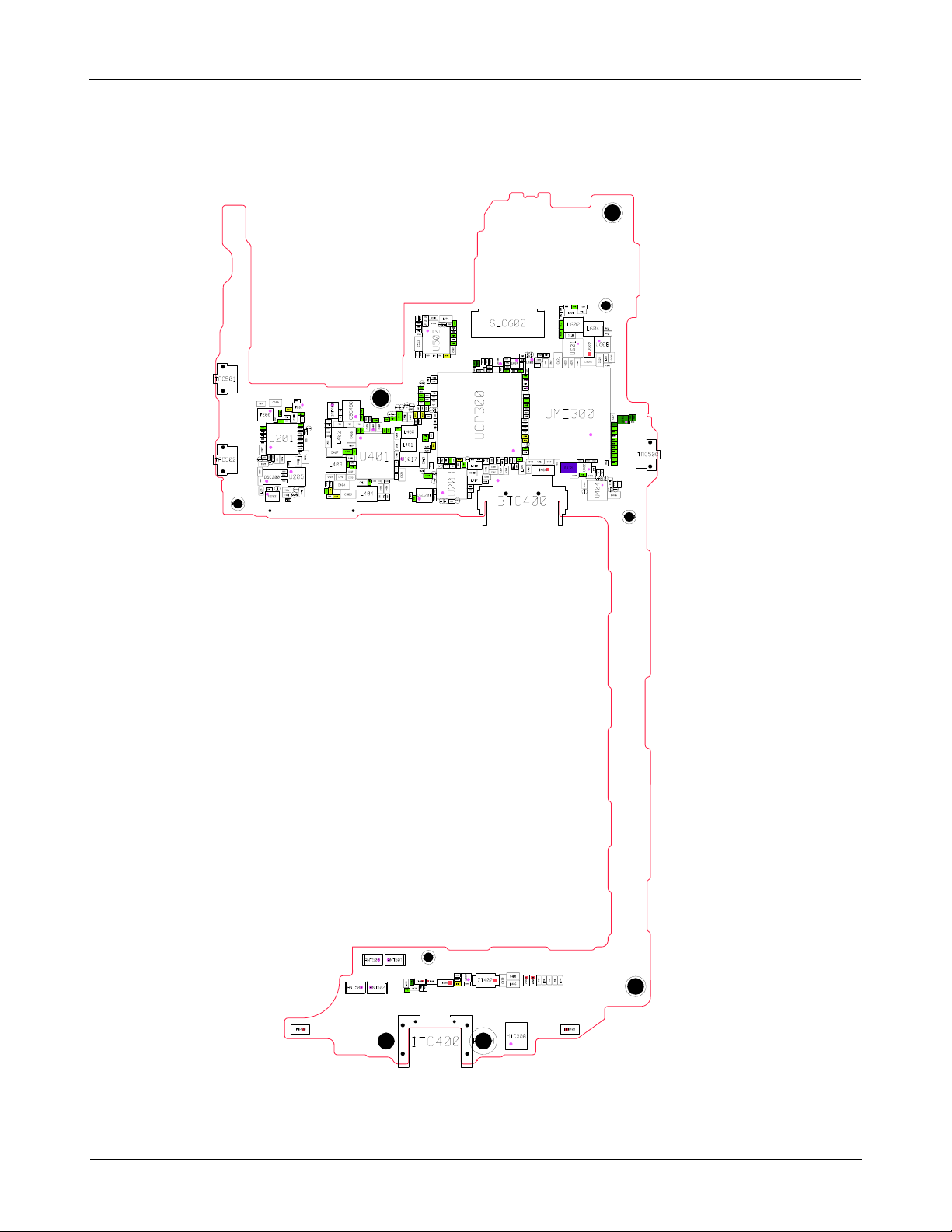
PCB Diagrams
8-2.
8-2-1.
Top
TAC501
TAC502
BH403
C532
F200
C229
C228
C221
C213
U201
C206
7
0
2
C
C272
TP_BT_DATA
TP_BT_SSBI
C225
9
3
5
C
OSC200
2
0
2
C
5
C251
1
2
L
U202
Level3Repair
BH400
C616
C647
BH402
C607
0
5
6
C
C617
L601
1
0
6
0
1
0
0
0
0
1
1
_
_
I
I
B
B
S
S
C612
C614
S
S
_
_
C613
P
P
T
T
C635
C648
0
9
6
5
U605
3
3
9
C634
4
C
C
6
C
7
2
R326
6
R
R325
U1018
C385
U1019
R329
C366
C398
C356
C357
C358
UME300
C373
C330
C331
C319
R323
R324
0
0
3
C
D
S
_
P
T
R327
C361
R415
C469
R1012
VR402
9
5
6
3
0
7
C
8
4
4
L
D400
C
C
0
1
6
L602
R
R611
L604
9
0
R612
6
R
C618
1
0
0
U608
0
6
6
D
U
7
3
2
0
2
1
2
3
6
2
6
C
C
0
7
4
C
R430
6
6
2
L
C
0
6
2
2
C626
6
C
6
3
C
C
C602
7
5
4
0
6
0
0
6
6
3
R
R
0
C
6
R510
Q
R603
R335
R339
R348
R336
R340
R342
R341
R337
TAC500
R338
C474
R432R433
1
1
R347
5
R
2
0
5
3
4
4
R
3
2
U
1
1
3
3
R
R
R431
T
P
C475
C473
N
D
I
_
_
C
B
I
S
TP_USB_DM
U
U
M
_
_
P
P
T
8
T
7
2
4
7
4
3
7
7
4
4
C
4
4
C
R
C
L
_
S
P
N
0
O
TP_VPS_R
V
_
T
_
O
P
O
B
T
_
T
R
A
U
4
_
P
T
C476
U
BH408
1
C512
3
4
0
C518
5
5
L
C
L501
C516
4
4
5
C542
C506
C
TP_CODEC_INTTP_CODEC_RST
C507
C511
C543
L508
C540
3
1
5
C
4
6
0
0
5
5
R
R
9
8
3
C
TP_UART_TX
R350
R344
R334
R346
R343
R349
R333
R345
TP_UART_RX
TP_SLIMBUS_CLK
1
1
5
TP_FM_DATA
TP_FM_SSBI
2
7
2
3
3
3
C
C
C
TP_SLIMBUS_DATA
TP_BT_STROBE
2
4
9
TP_WLAN_CLK
TP_WLAN_SET
2
2
4
4
4
7
8
R
R
4
C377
4
4
C
4
4
C413
C
C
C446
9
1
4
5
3
3
C
C
0
6
4
C450
0
1
C
1
1
4
4
C
C
L400
5
0
4
C461
C
C462
6
0
L401
4
R1023
C
R1024
2
8
4
C
3
8
U1017
4
4
1
4
C
R
7
2
4
C
TP_SWIO1
4
2
3
4
1
C453
4
R
C
C421
C426
0
9
2
1
4
4
C
C
4
0
7
1
3
4
0
2
2
OSC201
R
4
4
4
6
0
C
C
R
4
R
C459
C438
C437
C445
C402
L403
C439
4
3
4
C
1
4
4
C
BH405
0
0
0
0
4
4
9
8
2
2
4
T
4
C
C
C
A
S
0
7
B
3
1
3
4
4
4
4
4
C
R
4
4
C
C
C458
O
C436
C454
C456
5
0
3
0
4
4
5
6
C
U
1
1
4
4
C
C
6
2
6
4
0
C
4
5
5
L
4
C
C407
2
1
C409
4
C
C467
C408
U401
0
C433
4
4
C
C414
C457
C442
C425
8
C400
1
4
8
C417
C
6
4
C
C404
8
2
4
R
C403
L404
C422
R429
C237
C200
F201
R201
2
0
2
L
L214
8
1
C219
2
7
5
0
1
2
2
C
R
C
C214
C220
C247
C246
TP_WLAN_D0
7
1
2
C
C216
C209
4
2
2
C210
C
C211
C212
0
0
2
L
1
5
2
0
0
2
4
3
2
2
2
0
2
C
C
2
2
8
C
C
C
0
2
5
6
2
C
C
C203
R314
U205
R315
T
U
O
_
L
L
A
H
TP_ACC_INT_200
_
P
R351
T
8
6
2
C
TP_ACC_INT_201
C368
TH300
SLC602
L515
C509
2
C514
0
C517
C505
5
2
0
5
U
C
C521C523
L502
R503
C378
C384
R318
R319
R316
R317
0
0
3
K
L
C
M
_
M
A
C
_
P
T
5
6
3
C
2
8
3
C
3
8
3
C
3
2
3
C
1
0
4
R
0
1
3
0
1
7
8
6
1
1
3
3
4
3
3
C
C
C
R
R
3
7
2
TP_NFCFW
C249
L216
C
TP_NFC_INT
3
E
L
B
A
N
E
_
C
F
0
N
_
P
T
2
1
6
2
C
2
U
6
2
C
TP_NFC_VDDA
TP_NFC_MON200TP_NFC_MON201
C254
6
5
5
5
3
3
R
R
2
7
3
C
C379
0
0
3
P
C
U
TP_BBCLK300
R420
R320
C355
6
2
8
5
4
2
C
C
L218
C248
L217
C255
C250
3
5
2
C
C633
0
6
6
2
0
0
2
3
6
6
6
6
R
R
C
R631
U604
U
R632
C336
1
2
3
3
3
3
R
R
C375
R359
C337
4
0
4
2
2
0
6
2
2
7
2
5
8
7
3
3
3
3
3
3
3
2
C
C
C
C
C
C
C
5
3
R
1
0
3
H
C260
8
T
9
3
5
5
6
2
2
2
C
C
C
C257
C256
R208
BTC400
ANT500 ANT501
ANT502ANT503
LED400 LED401
BH407
1
8
ZD400 ZD401
5
4
0
C
5
L
7
8
3
3
4
4
R439
R
R
C531
IFC400
2
R607
0
C480
9
0
9
6
C600
D500
L519
U
ZD402
C609
BH404
7
4
C
MIC500
1
3
4
0
1
0
1
0
0
0
0
2
5
5
5
5
5
5
5
L
L
C
C
C
D
D
Z
Z
L406
BH406
8-2
Confidential and proprietary-the contents in this service guide subject to change without prior notice.
Distribution, transmission, or infringement of any content or data from this document without Samsung’swritten authorization is strictly prohibited.
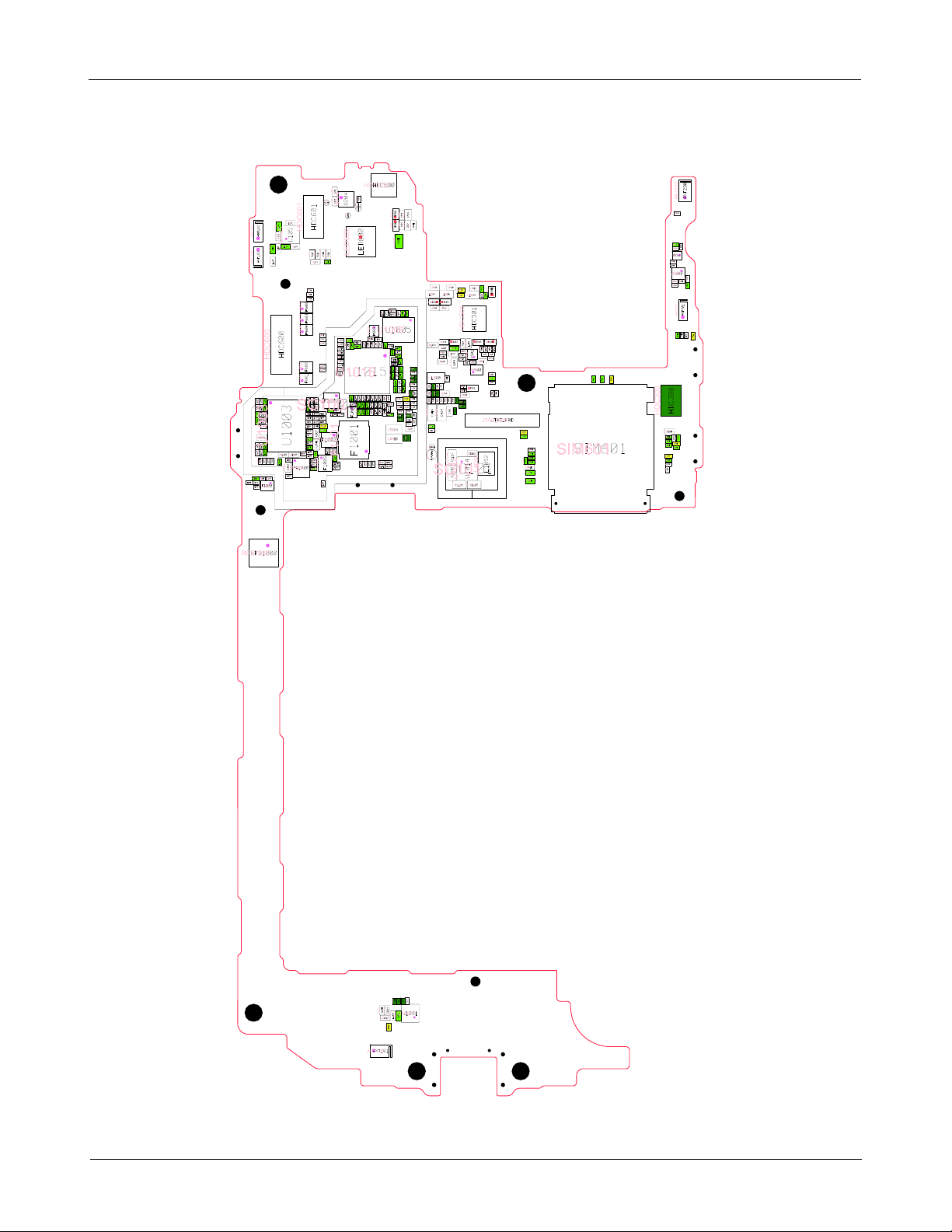
Level3Repair
8-2-2.
Bottom
8-3
Confidential and proprietary-the contents in this service guide subject to change without prior notice.
Distribution, transmission, or infringement of any content or data from this document without Samsung’swritten authorization is strictly prohibited.
8-3.
8-3-1.
Level3Repair
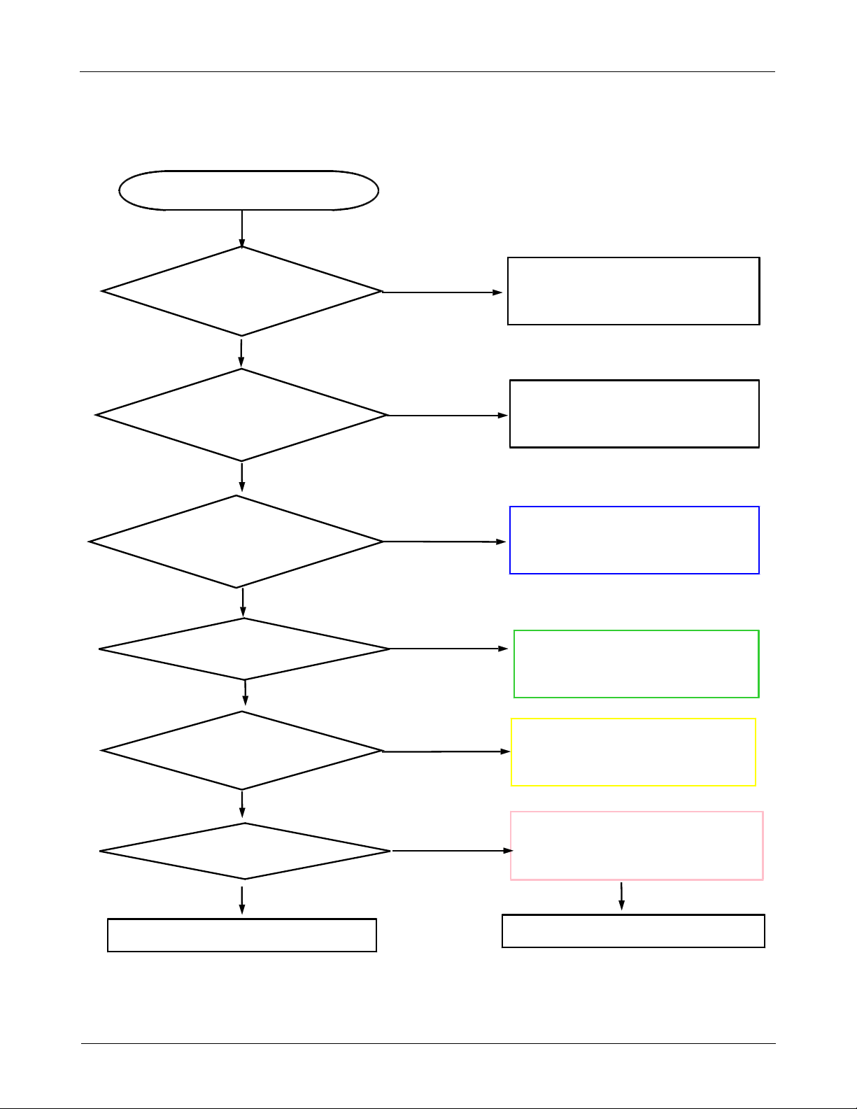
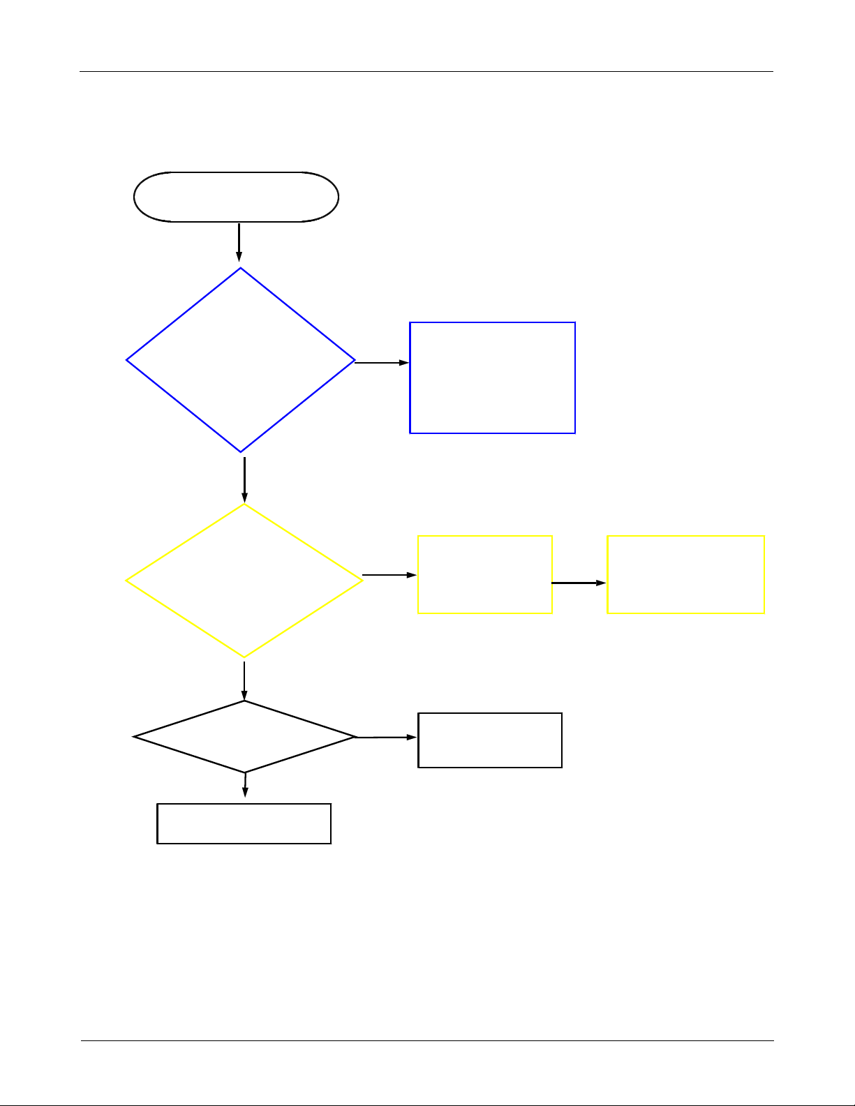
LOGIC
Power On
Power switch on
NG
Connect the jig box.
Check the current consum
ption
>= 100
mA?
Yes
Check the battery
voltage
>= 3.45?
Yes
Check the GPIO_25
of UCP300-1 PS_H
OLD pin is
1.85
V?
Yes
Check the clock at
OSC400
=19.2
MHz
NO
\
NO
NO
Download
Change the battery
Check the PMIC
relatedtoPS_HOLD
NO
?
Resolder OSC400
Yes
C464(VREG_S1)=1.15V?
C465(VREG_S2)=1.15V?
C466(VREG_S3)=1.3V?
C467(VREG_S4)=2.1V?
NO
Check the voltage and ResolderU
401
Yes
check
the initial operation
Yes
END
Confidential and proprietary-the contents in this service guide subject to change without prior notice.
Distribution, transmission, or infringement of any content or data from this document without Samsung’swritten authorization is strictly prohibited.
NO
8-4
Resolder or Replace UCP300
NO
Change the main PBA
Level3Repair
VREG_S1_1P15
C303
C308
C315
C310
C309
C316 C317
C311
C318
7
1
1
2
3
2
P
P
P
A
A
A
D
D
D
N
N
N
G
G
G
AA16
VDD_CORE
AA18
VDD_CORE
AA22
VDD_CORE
AA24
VDD_CORE
AA30
VDD_CORE
AB21
VDD_CORE
AB23
VDD_CORE
AB27
VDD_CORE
AB29
VDD_CORE
AC14
VDD_CORE
AC16
VDD_CORE
AC24
VDD_CORE
AC30
VDD_CORE
AD13
VDD_CORE
AD15
VDD_CORE
AD21
VDD_CORE
AE14
VDD_CORE
AE16
VDD_CORE
AE18
VDD_CORE
AE24
VDD_CORE
AE30
VDD_CORE
AE32
VDD_CORE
AF21
VDD_CORE
AG18
VDD_CORE
AG26
VDD_CORE
AH21
VDD_CORE
AJ14
VDD_CORE
AJ20
VDD_CORE
AJ26
VDD_CORE
AJ30
VDD_CORE
AK11
PMIC_SPMI_DATA
PMIC_SPMI_CLK
VREG_L6_1P8
C386
C387
7
2
3
R
MSM_RESOUT_N
MSM_RESIN_N
MSM_PS_HOLD
CAM_ANALOG_EN
CAM_IO_EN
MOTOR_EN
MODE_1
MODE_0
TP_MSM_RESIN_N
AT7
AR6
E32
D33
C34
D27
G28
F25
C26
D25
C24
C2
AV31
AU32
RFFE1_DATA
RFFE1_CLK
RESOUT_N
RESIN_N
PS_HOLD
PMIC_SPMI_DATA
PMIC_SPMI_CLK
SPI_CS3_N_BLSP3
SPI_CS3_N_BLSP2
SPI_CS2_N_BLSP3
SPI_CS1_N_BLSP3
SPI_CS1_N_BLSP2
MODE_1
MODE_0
GPIO_100
GPIO_99
// No-Pull_up //
GPIO_112
GPIO_114
{ MPM_interrupt }
GPIO_111
// No-Pull_up //
// No-Pull_up //
{ MPM_interrupt }
GPIO_110
// No-Pull_up //
{ MPM_interrupt }
GPIO_113
}
}
}
}
}
}
}
}
}
t
t
t
t
t
t
t
t
t
p
p
p
p
p
p
p
p
p
u
u
u
u
u
u
u
u
u
r
r
r
r
r
r
r
r
r
r
r
r
r
r
r
r
r
r
e
e
e
e
e
e
e
e
e
t
t
t
t
t
t
t
t
t
n
n
n
n
n
n
n
n
n
i
i
i
i
i
i
i
i
i
_
_
_
_
_
_
_
_
_
M
M
M
M
M
M
M
M
M
P
P
P
P
P
P
P
P
P
M
M
M
M
M
M
M
M
M
{
{
{
{
{
{
{
{
{
6
4
_
O
I
P
G
K
L
C
S
_
4
_
S
2
I
M
9
7
2
8
7
1
9
0
3
4
5
6
4
6
5
4
5
6
_
_
_
_
_
_
_
_
_
O
O
O
O
O
O
O
O
O
I
I
I
I
I
I
I
I
I
P
P
P
P
P
P
P
P
P
G
G
G
G
G
G
G
G
G
K
K
K
L
L
L
S
S
S
C
0
1
0
C
C
W
S
D
D
S
D
W
W
M
_
_
_
_
_
_
_
_
_
2
1
3
3
3
4
4
3
1
_
_
_
_
_
_
_
_
_
S
S
S
S
S
S
S
S
S
2
2
2
2
2
2
2
2
2
I
I
I
I
I
I
I
I
I
M
M
M
M
M
M
M
M
M
0
9
4
3
C
D
A
A
VPH_PWR
VREG_S4_2P1
VREG_L25_2P075
C413C410 C412C411
VREG_S3_1P3
C415C414
C416
VDD_GR1
VDD_GR2
VDD_GR3
VDD_GR4
VDD_GR5
VDD_GR6
VDD_GR7
8-5
Confidential and proprietary-the contents in this service guide subject to change without prior notice.
Distribution, transmission, or infringement of any content or data from this document without Samsung’swritten authorization is strictly prohibited.
Level3Repair
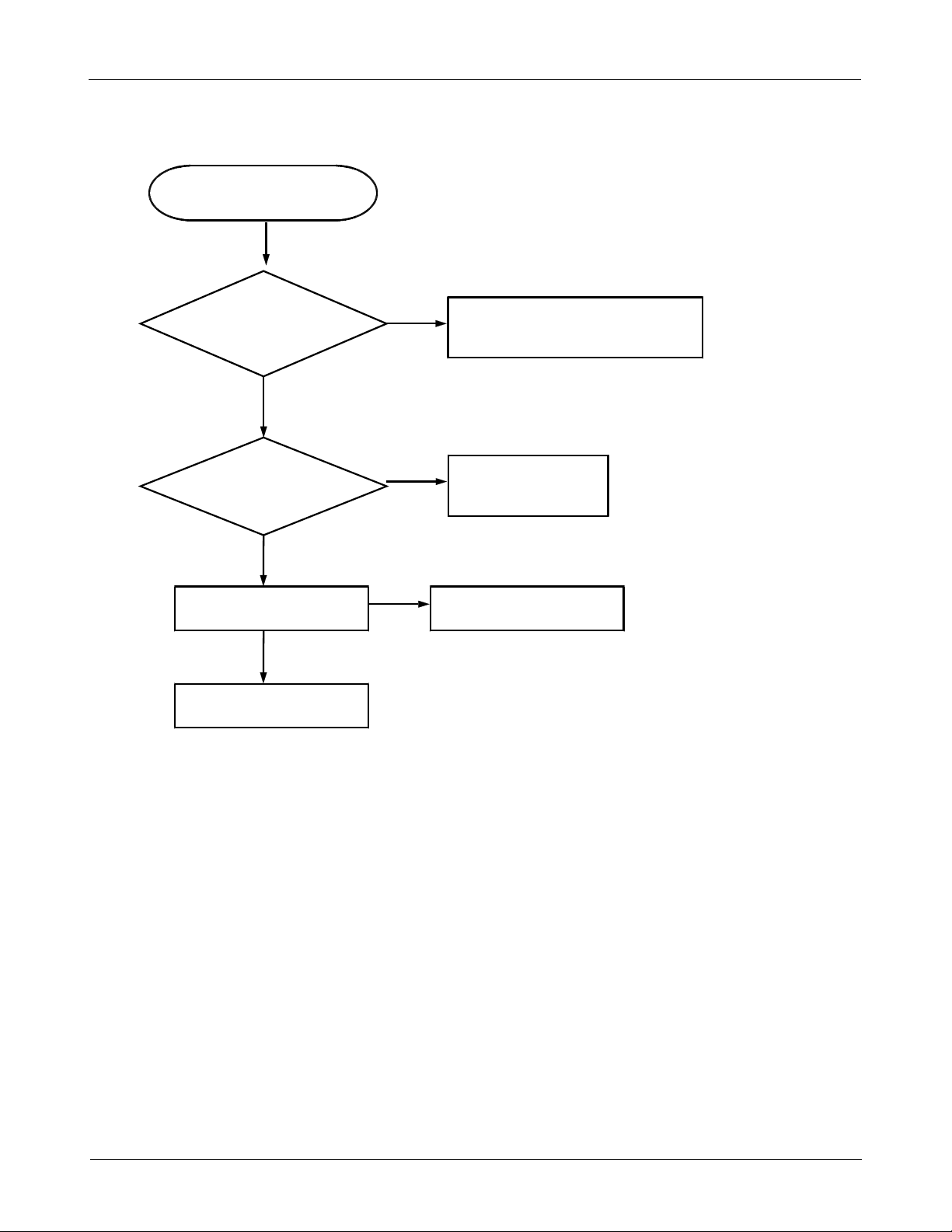
8-3-2.
LCD Working
Power Switch On
LCD Display
On?
Yes
NO
LCD FPCB
connector is co
rrectly connecti
ned?
Yes
Correctly connected
NO
C618
LED_P_26V=26V?
Yes
CHECK
LCD DATALINE
LCD_SDA,SCL)
(
Replace U603&Check
D600,L602,L601,L603
NO
Resolder or replace UCP300
NO
Replace or Resolder
&
D600,L602,L601,L603
Yes
Replace LCD
Confidential and proprietary-the contents in this service guide subject to change without prior notice.
Distribution, transmission, or infringement of any content or data from this document without Samsung’swritten authorization is strictly prohibited.
NO
Replace PBA
8-6
Level3Repair
A
L
LCD_ON
LCD_PWM_BL
MIPI_DSI0_DATA3_M
MIPI_DSI0_DATA3_P
MIPI_DSI0_DATA0_M
MIPI_DSI0_DATA0_P
MIPI_DSI0_CLK_M
MIPI_DSI0_CLK_P
MIPI_DSI0_DATA1_M
MIPI_DSI0_DATA1_P
MIPI_DSI0_DATA2_M
MIPI_DSI0_DATA2_P
LCD_PWM_BL
VPH_PWR_BLU
R611R612
VDD_TSP_2.8V
HDC600
22
11
44
55 66
7788
99
10 10
11 11 12 12
13 14
13
15
17
19
23
25 26
27
29
33
C627
14
15 16
16
17 18
18
19
20
20
212122
22
24
23
24
25
26
27 28
28
293330
30
313132
32
33 34
34
NCNC36NC
NC
35
3738
L604
2
1
C
B
N
I
V
CTRL
PWM
U608
D
D
N
N
C
G
N
G
1
2
2
1
C
B
A1
A2 A3
VSN_-5.0V
X
L
VOUT
C
N
VSP_5.0V
TSP_VDD_1.8V
R600
R601 R602
VCC_1.8V_LCD
TS_INT_N
TS_I2C_SC
TS_I2C_SD
DSI_RST_N
LED_A_20V
LED_K1
LED_K2
VGH
C605
D600
C3
S1
B3
S2
C606C604 C607
LED_K2
LED_K1
C647
C622
L603
LED_A_20V
C602
8-7
Confidential and proprietary-the contents in this service guide subject to change without prior notice.
Distribution, transmission, or infringement of any content or data from this document without Samsung’swritten authorization is strictly prohibited.
Level3Repair
8-3-3.
TSP
Operate TSP
NG
Check
TSP Connecting
YES
Check
LCD Connecting
YES
Check
VTOUCH_3.0V
NO
NO
NO
Reconnecting TSP
Reconnecting LCD
Resolder or Replace
PM400
YES
Check
TSP_SCL,SDA
YES
Replace LCD
NO
NO
Resolder or Replace
UCP300
Replace PBA
8-8
Confidential and proprietary-the contents in this service guide subject to change without prior notice.
Distribution, transmission, or infringement of any content or data from this document without Samsung’swritten authorization is strictly prohibited.
Level3Repair
8-3-4.
Audio Working
Speaker Working
Operate speaker
NG
Signal on in
SPK_OUT_P
SPK_OUT_N?
&
YES
NO
Resolder
ZD507,ZD508
C508,C527
Signal on in
L506,L507
?
YES
Speaker break
down?
NO
Change main PBA
NO
YES
Resolder
L506, L507
Replace PM8226
Change Speaker
NO
Resolder or
Replace UCP300
8-9
Confidential and proprietary-the contents in this service guide subject to change without prior notice.
Distribution, transmission, or infringement of any content or data from this document without Samsung’swritten authorization is strictly prohibited.
Level3Repair
_
EAR_ADC_3.5
L523
VDD_MIC_BIAS2_2.8V
R518
R520
EAR_DETECT_MIC
EAR_DETECT_GND
L506
L507
C529
C530
R514
C546
3
4
0
0
5
C545
5
D
D
Z
Z
HDC501
1
2
1
2
334
L509
L510
C534
4
556
6
78
7
8
99
10
10
NC
NC
NCNC
1213
14
11
ZD507
L511
L513
C538
C537
5
6
0
0
5
5
D
D
Z
Z
C535
C536
EARSPK_R
EARSPK_L
R502
R516
C515
ZD508
R517
FM_ANT
L514
HPH_REF
C522
L504
R523
R513
EAR_MIC_3.5
SPK_OUT_P
SPK_OUT_N
R519
EAR_MIC_3.5_P
EAR_DETECT_EARLEFT
C533
8-10
Confidential and proprietary-the contents in this service guide subject to change without prior notice.
Distribution, transmission, or infringement of any content or data from this document without Samsung’swritten authorization is strictly prohibited.
Level3Repair
Receiver Working
Operate Receiver
NG
Check
ZD501,ZD502,
C524,C525
YES
Receiver break
down?
NO
Check
UCP300
YES
Change main PBA
NO
YES
NO
Resolder or Replace
ZD501,ZD502,C524,C525
Change Receiver
Resolder or Replace
UCP300
8-11
Confidential and proprietary-the contents in this service guide subject to change without prior notice.
Distribution, transmission, or infringement of any content or data from this document without Samsung’swritten authorization is strictly prohibited.
Level3Repair
MICW
orking
Operate MIC
NG
Pollute
MIC Hole?
NO
Signal on in
C501, C503,
C504?
YES
YES
NO
Clean up
MIC hole
Resoldering
C501, C503, C504
MIC
break down
NO
Check Voltage
of
L500
is
1.8V ?
Voltage
YES
CrashU502IC?
YES
YES
Resolder or Replace
MIC
NO
Change UCP300
NO
Change main PBA
8-12
Confidential and proprietary-the contents in this service guide subject to change without prior notice.
Distribution, transmission, or infringement of any content or data from this document without Samsung’swritten authorization is strictly prohibited.
Level3Repair
M
MIC500
POWER1POWER
GND1
GND2
OUT
VDD_MIC_BIAS1_1.8V
GND
2
GND
3
OUT
4
L500
L521
MAIN_MIC_
MAIN_MIC_P
C504C503 ZD509
L502
R503
EAR_MIC_M
C521
C513
C501
VDD_MIC_BIAS2_2.8V
R504
R506
C523
ZD510
EAR_MIC_3.5_P EAR_MIC_P
EAR_MIC_3.5_M
8-13
Confidential and proprietary-the contents in this service guide subject to change without prior notice.
Distribution, transmission, or infringement of any content or data from this document without Samsung’swritten authorization is strictly prohibited.

Stereo Headset Working
Hands-free stereo
headset
NG
Level3Repair
Button NG?
NO
MIC NG?
NO
SPK NG?
YES
YES
YES
Resolder or Replace
U500,U501
Check
L507
YES
Reconnect HDC501
Signal on
in L511 L513
NO
Check U500,U501
NO
Resolder or Replace
L511 L513
YES
NO
Resolder or Replace
PM8226
The End
8-14
Confidential and proprietary-the contents in this service guide subject to change without prior notice.
Distribution, transmission, or infringement of any content or data from this document without Samsung’swritten authorization is strictly prohibited.

Level3Repair
EARSPK_L
EARSPK_R
HPH_REF
EAR_ADC_3.5
SPK_OUT_P
VDD_MIC_BIAS2_2.8V
L523
SPK_OUT_N
R518
R519
EAR_MIC_3.5_P
R520
EAR_DETECT_EARLEFT
C533
L506
L507
C530
C529
EAR_DETECT_MIC
EAR_DETECT_GND
R514
VDD_CODEC_BUCK_2.1V
C545
L510
C546
3
4
0
0
5
5
D
D
Z
Z
L509
C534
VDD_CODEC_DIG_1.2V
HDC501
1
2
1
2
334
4
556
6
7
78
8
10
99
10
NC
NC
NCNC
1213
14
11
ZD507
5
0
5
D
Z
L511
L513
C538
C537
6
0
5
D
Z
VPH_PWR_SPKDRV
EARSPK_R
EARSPK_L
C535
C536
R502
R516
C515
ZD508
R517
L514
L504
R513
FM_ANT
HPH_REF
C522
R523
EAR_MIC_3.5_M
VDD_CODEC_IO_1.8V
VPH_PWR
C506
D
N
G
_
K
C
U
B
_
C
E
D
O
C
L503
L508
L515
C540
C544
C541
C543
C542
RCV_N
RCV_P
VPS_L
VPS_R
SPK_OUT_N
SPK_OUT_P
MAIN_MIC_M
MAIN_MIC_P
EAR_MIC_M
EAR_MIC_P
SLIMBUS_CLK
SLIMBUS_DATA
C507
TP_SLIMBUS_CLK
TP_SLIMBUS_DATA
31
26
16
21
17
36
32
50
49
39
44
53
47
43
38
41
42
46
52
37
20
30
C509
EAROM
EAROP
HPH_L
HPH_R
HPH_REF
LINE_OUT1
LINE_OUT2
SPKR_DRVM
SPKR_DRVP
MIC1_INM
MIC1_INP
MIC2_INM
MIC2_INP
MIC3_INM
MIC3_INP
MIC4_INM
MIC4_INP
MIC5_INM
MIC5_INP
MBHC_HSDET
SLIMBUS_CLK
SLIMBUS_DATA
5
5
0
5
7
9
3
4
3
2
1
1
O
I
G
I
T
K
_
X
V
D
A
C
D
R
_
R
B
_
U
D
D
V
D
X
B
V
_
D
T
K
_
D
_
V
P
D
D
D
S
D
_
V
D
V
D
V
D
V
U502
WCD9306
V
V
R
R
T
K
D
D
L
C
I
K
K
F
U
P
P
B
S
C
S
_
_
_
_
D
D
D
D
D
D
D
D
N
N
N
N
N
N
N
N
G
G
G
G
G
G
G
G
8
5
0
3
5
8
7
2
5
4
2
2
1
DMIC0_CLK
DMIC0_DATA
DMIC1_CLK
DMIC1_DATA
NCP_C1M
NCP_VNEG
BUCK_VOUT1
BUCK_VOUT2
BUCK_VSW
LDO_HI_CAP
MIC_BIAS1
MIC_BIAS2
MIC_BIAS3
C
N
7
6
5
5
NCP_C1P
CCOMP
RESET_N
C
N
C502
C505
D
N
G
_
V
R
D
K
P
S
9
24
15
14
C511
1
2
11
6
12
13
L501
34
54
48
51
22
29
MCLK
33
MODE
8
4
INTR
C516
C512
D
N
G
_
K
C
U
B
_
C
E
D
O
C
TP_CODEC_RST
TP_CODEC_INT
C518
C517
VDD_MIC_BIAS2_2.8V
VDD_MIC_BIAS1_1.8V
CODEC_RESET_N
CODEC_INT_N
PMIC_AUDIO_REF_CLK
C514
8-15
D
N
D
G
N
_
V
G
_
R
K
D
C
K
U
P
B
S
_
C
E
D
O
C
D
N
G
_
K
C
U
B
_
C
E
D
O
C
Confidential and proprietary-the contents in this service guide subject to change without prior notice.
Distribution, transmission, or infringement of any content or data from this document without Samsung’swritten authorization is strictly prohibited.

Level3Repair
8-3-5.
KEY Working
Power KEY
Press Power Key
Check the P/K
Soldering State
It is OK
YES
Check
R510
NG
?
NO
NO
Resoldering the TAC
Resolder or Replace
R510
500
YES
Check
ON_SW
YES
Change main PBA
NO
Resolder or Replace
UCP300
8-16
Confidential and proprietary-the contents in this service guide subject to change without prior notice.
Distribution, transmission, or infringement of any content or data from this document without Samsung’swritten authorization is strictly prohibited.

Level3Repair
Volume Key and Oter Sub key
Press Volume Key
and Other Sub Key
Volume Key NG?
NO
home Key
NG?
NO
Yes
Yes
Resolder or Replace TAC501, TAC502
Resolder or Replace
R511,L505,ANT502,ANT503
Yes
Resolder or Replace UCP300
Yes
Replace PBA
home Key LED
NG?
Yes
Check LED400, LED401 is damaged
NO
Menu&Back Key
NG?
Confidential and proprietary-the contents in this service guide subject to change without prior notice.
Distribution, transmission, or infringement of any content or data from this document without Samsung’swritten authorization is strictly prohibited.
GO TO
8-17
8-3-3.
TSP

TAC501
TAC500
Level3Repair
R510
12
34567
12
7
3456
C532
PM_KYPD_PWR_N
PM_RESIN_N
VOL_UP_KEY
OK_KEY
VREG_L6_1P8
R511
L505
C531
1
1
ANT502
2
2
1
1
ANT503
2
2
TAC502
12
34567
VOL_DOWN_KEY
C539
8-18
Confidential and proprietary-the contents in this service guide subject to change without prior notice.
Distribution, transmission, or infringement of any content or data from this document without Samsung’swritten authorization is strictly prohibited.

Level3Repair
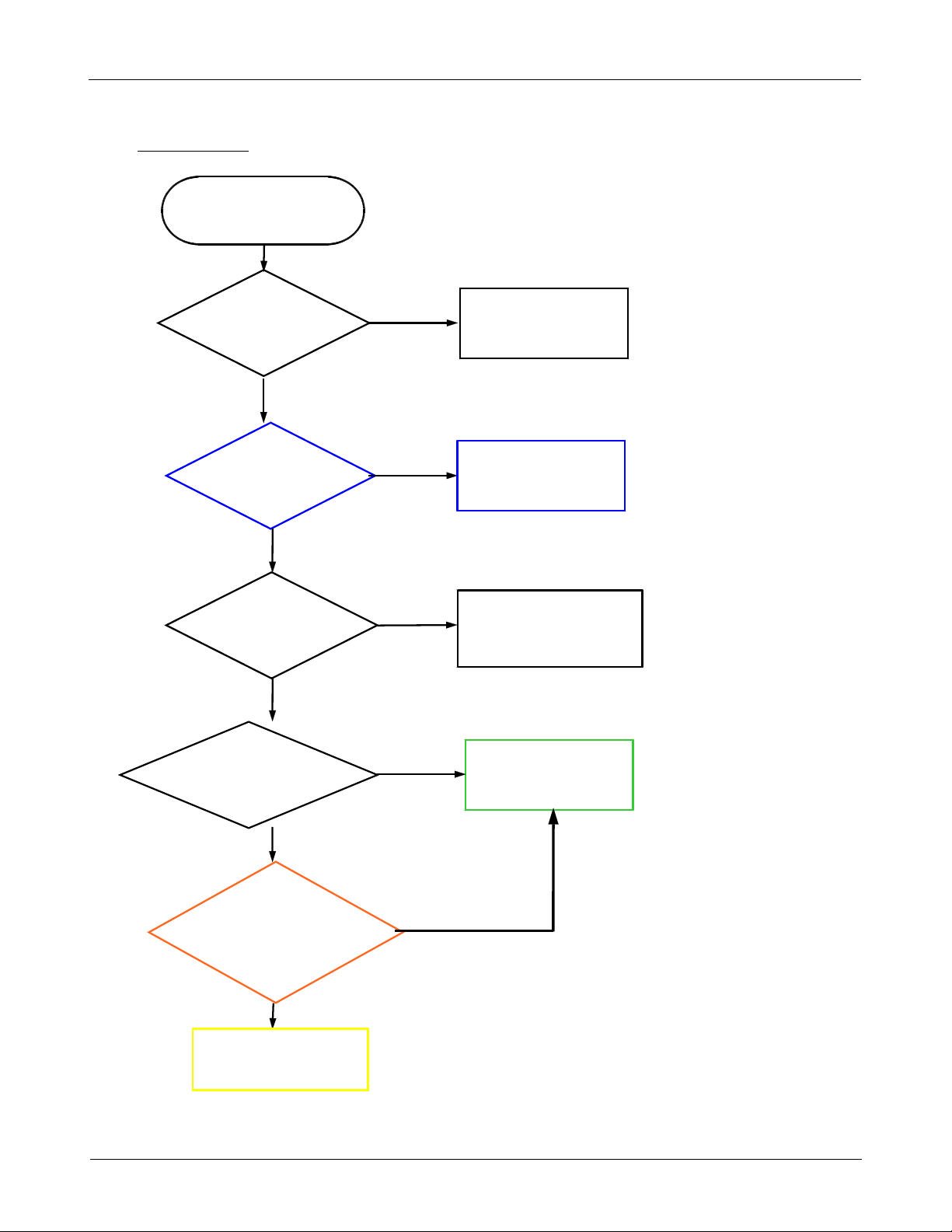
8-3-6.
Vibrator Working
Operate Vibrator
Check
Vibrator Motor
Check
D500,L519
NO
Yes
Yes
NO
No
Resolder Vibrator Motor
Resolder or Replace
D500,L519
VDD_MOTOR_3.3V
L519)
(
=3.3
V?
NO
Check Motor LDO
and PM8226.
8-19
Confidential and proprietary-the contents in this service guide subject to change without prior notice.
Distribution, transmission, or infringement of any content or data from this document without Samsung’swritten authorization is strictly prohibited.

V
ANT200
N
1
1
2
2
C226
C243
C233
C244
F202
14
L209
C234
OUT
IN
G
G
G
2
3
5
L205
1
GND
2
GND
RFIN3VDD
VDD_FEM/GPS_2.75
U200
6
RFOUT
5
EN
4
C241
C230
C235
GPS_EXT_CTRL
C245
C239
1
F203
IN
Level3Repair
C236
4
OUT
G
G
G
5
3
2
L206
GPS_RF_I
C240
L210
8-20
Confidential and proprietary-the contents in this service guide subject to change without prior notice.
Distribution, transmission, or infringement of any content or data from this document without Samsung’swritten authorization is strictly prohibited.

Level3Repair
8-3-7.
T-Flash Card Working
Insert&Operate
microSD card
SIM601
break down
nd Pin of
2
SIM601
=
High
NG
NO
?
YES
?
Change SIM601
YES
Change SIM601
st Pin of
1
SIM601
=3.0V?
YES
Check
UCP300
NO
NO
Resolder or Replace
PM8226(PMIC)
8-21
Confidential and proprietary-the contents in this service guide subject to change without prior notice.
Distribution, transmission, or infringement of any content or data from this document without Samsung’swritten authorization is strictly prohibited.

Level3Repair
A
UIM1_RESET
UIM1_CLK
NFC_SWP
UIM1_DATA
VDD_UIM1_3.0V
8
7
3
3
6
6
C
C
UIM2_RESET
UIM2_CLK
VDD_UIM1_3.0V
8
1
6
R
9
3
6
C
R613
T_FLASH_D(2)
T_FLASH_D(3)
T_FLASH_CMD
T_FLASH_CLK
T_FLASH_D(0)
T_FLASH_D(1)
6
3
6
C
VDD_UIM1_NFC
R614
R624
VDD_UIM2_3.0V
1
2
4
4
6
6
C
C
VDD_TFLASH_2.95V
0
4
6
C
T_FLASH_DETECT_N
C643
SIM600
C1
C2
C3
VREG_L21_2P95
R619
C1
C2
C3
GG
23GG4
1
R620
R621
VDD_UIM2_3.0V
C5
C5
C6
C6
C7
C7
VREG_L6_1P8
C629
R615
R623
R622
R630
C644
9
2
6
R
SIM601
1
S1_VCC
2
S2_RST
3
S3_CLK
4
S4
5
S5_GND
6
S6_VPP
7
S7_IO
8
S8
9
T1_DAT2
10
T2_CD_DAT3
11
T3_CMD
12
T4_VDD
13
T5_CLK
14
T6_VSS
15
T7_DAT0
16
T8_DAT1
17
G1
18
G2
19
G3
20
G4
21
G5
22
G6
23
G7
24
G8
25
DETECT
UIM2_DAT
U609
0
5
U
0
C
4
4
6
R
3
0
C
C
C
C
3
3
3
3
3
3
3
3
2
4
5
3
C
1
9
6
1
0
6
D
0
C
3
4
R
0
8
6
2
3
4
1
1
1
3
3
3
C
C
C
C
C
C
C
C
C
3
3
3
3
3
3
1
1
1
5
8
7
0
4
3
1
5
0
3
3
3
C
C
C
C
6
3
8
C
7
3
8
K
L
C
_
P
E
E
L
S
_
P
T
N
_
R
N
_
ESI
M
S
M
T
_
P
C
6
4
4
0
5
5
9
0
3
8
4
4
C
8
1
6
0
1
1
3
3
3
C
C
C
6
R
1
5
6
R
3
0
5
R
R
6
6
2
2
2
3
D
A
_
P
J
G
T
A
S
6
0
I
M
0
4
9
4
R
0
1
3
9
9
9
4
4
4
R
R
R
0
0
3
C
D
H
R
1
9
6
R
2
0
6
R
2
1
S
I
M
6
0
1
6
C
6
4
3
R
2
4
6
C
6
3
7
6
3
R
1
R
4
6
1
C
6
6
3
8-22
Confidential and proprietary-the contents in this service guide subject to change without prior notice.
Distribution, transmission, or infringement of any content or data from this document without Samsung’swritten authorization is strictly prohibited.

Level3Repair
8-3-8.
SIM Card Working
Insert&Operate
R629,U609
SIM card
NG
SIM Connector
Break down?
YES
R618,C639
=3.0V
NO
Change SIM600,SIM601
No
Check PM8226(PMIC)
YES
Resolder SIM600,SIM601
Yes
Check data,clk,reset line
Yes
Change PBA
No
Resolder or Replace
PM8226
8-23
Confidential and proprietary-the contents in this service guide subject to change without prior notice.
Distribution, transmission, or infringement of any content or data from this document without Samsung’swritten authorization is strictly prohibited.

Level3Repair
UIM1_RESET
UIM1_CLK
NFC_SWP
UIM1_DATA
VDD_UIM1_3.0V
VREG_L21_2P95
VDD_UIM1_NFC
R613
T_FLASH_D(2)
T_FLASH_D(3)
T_FLASH_CMD
T_FLASH_CLK
T_FLASH_D(0)
T_FLASH_D(1)
6
3
6
C
R614
VDD_TFLASH_2.95V
R621
R619
R620
R624
VDD_UIM1_3.0V
8
1
6
R
7
8
3
3
6
6
C
C
9
3
6
C
C629
T_FLASH_DETECT_N
C643
U
5
0
0
4
C
4
6
0
R
3
C
C
C
C
3
3
3
3
3
3
3
3
3
2
4
5
9
C
1
6
D
6
0
1
3
0
C
4
8
R
0
4
1
3
C
C
3
1
8
3
0
3
C
6
2
3
1
1
3
3
C
C
C
C
C
C
C
3
3
3
3
3
6
C
4
4
0
1
1
5
5
5
9
7
3
0
4
4
8
0
4
1
5
3
3
C
C
C
6
8
1
1
0
1
3
3
3
C
C
C
6
5
R
1
6
R
3
0
5
R
R
6
6
2
2
3
2
D
A
P
_
G
A
J
T
VREG_L6_1P8
R615
R622
R623
R630
C644
0
3
4
1
9
9
9
4
R
9
4
4
4
R
R
R
10
11
12
13
14
15
16
17
18
19
20
21
22
23
24
25
1
2
3
4
5
6
7
8
9
SIM601
S1_VCC
S2_RST
S3_CLK
S4
S5_GND
S6_VPP
S7_IO
S8
T1_DAT2
T2_CD_DAT3
T3_CMD
T4_VDD
T5_CLK
T6_VSS
T7_DAT0
T8_DAT1
G1
G2
G3
G4
G5
G6
G7
G8
DETECT
0
0
3
C
D
H
6
C
8
3
7
C
8
3
6
0
M
1
S
I
K
L
C
_
P
E
E
L
S
_
P
T
I
N
S
_
S
_
N
R
_
E
M
M
P
T
0
0
S
6
I
M
9
R
1
6
0
R
2
6
1
R
2
6
6
C
4
3
4
R
2
6
7
C
3
6
3
R
1
6
4
R
1
6
6
3
6
C
8-24
Confidential and proprietary-the contents in this service guide subject to change without prior notice.
Distribution, transmission, or infringement of any content or data from this document without Samsung’swritten authorization is strictly prohibited.

Level3Repair
8-3-9
CAMERA Working
CAM
8M
Operate CAMERA
Camera connector
is connected correct?
C612
C613
C614
C616
NG
Yes
=2.8V
=2.8V
=1.8V
=1.25V
NO
NO
Re-connect
Check
PM8226(PMIC)
U600, U604(LDO)
&
Yes
CAM_MCLK(C605)
=24
MHz
?
Yes
Re-assy or replace the
camera module
NO
Change UCP300
8-25
Confidential and proprietary-the contents in this service guide subject to change without prior notice.
Distribution, transmission, or infringement of any content or data from this document without Samsung’swritten authorization is strictly prohibited.

Level3Repair
C
V
VDD_CAM_IO_1.8V
VDD_CAM_CORE_1.25V
HDC602
36
NC
2
1
2
1
4
3
4
3
5
6
CAM1_RST_N
MIPI_CSI0_DATA3_M
MIPI_CSI0_DATA2_P MIPI_CSI0_DATA2_M
MIPI_CSI0_CLK_P
MIPI_CSI0_DATA1_P MIPI_CSI0_DATA1_M
MIPI_CSI0_DATA0_M
CIS_SPI_SSN CIS_SPI_MISO
CIS_SPI_MOSI
C616
C614
56
7
788
9
10
9
11
11 12
131314
15
15 16
17
17 18
19
19
20
21
21 22
23
23 24
25
25 26
27
28
27
29
29
30
31 32
31
32
33 34
33
34
35
35
NC
10
12
14
16
18
20
22
24
26
28
30
37
VDD_CAM_SENSOR_A2.8V
VDD_CAM_AF_2.8V
C612
C613
D601
AF_SDAAF_SCL
CAM_I2C_SCLCAM_I2C_SDA
MAIN_CAM_MCLK
MIPI_CSI0_DATA3_P
MIPI_CSI0_CLK_M
MIPI_CSI0_DATA0_P
CIS_SPI_SCLK
MIPI_CSI1_CLK_M
MIPI_CSI1_DATA0_M
MIPI_CSI1_DATA0_P
HDC601
2
2
4
4
6
6
8
8
10
10
12
12
2020
4
2
VDD_CAM_SENSOR_A2.8V
VDD_CAM_IO_1.8V
1
1
3
3
5
5
7
7
9
9
11
11
13131414
15151616
171718 18
19
19
C
C
C
C
N
N
N
N
3
2
1
2
2
2
TP600
CAM_I2C_SCLMIPI_CSI1_CLK_P
CAM_I2C_SDA
CAM2_RST_N
C608
C610
VT_CAM_M
C651
CAM_IO_EN
CAM_ANALOG_EN
VPH_PWR
VPH_PWR
VDD4VOUT
3
CE
C632
4
VDD
3
CE
C649
R606
R626
R631
R632
VDD_LDO_IO_1.8V
U600
1
2
GND
D
N
G
5
C633
VDD_LDO_CAM_A2.8
U604
1
VOUT
2
GND
D
N
G
5
C648
8-26
Confidential and proprietary-the contents in this service guide subject to change without prior notice.
Distribution, transmission, or infringement of any content or data from this document without Samsung’swritten authorization is strictly prohibited.

Level3Repair
8-4-1.
GSM850/900/DCS/PCS Rx/WCDMA B1,2,5,8 RX/LTE B1,3,5,8,20
Channel
PCS),
665(
Check C1009
Check the Voltage at
C1002=VDD_RF
Check L1000,C1007,L1015,L102
Continuous Rx ON
GSM850),
: 190(
B1),
10700(
Cell power
≤
L1031
2,
dBm
-65
≥
-65
9800(
dBm
No
Yes
?
EGSM900),
62(
B2),
:-50
?
?
4400(
dBm
B5),
698(
3013(
DCS),
B8)
Yes
No
No
F1000 C1125,C1009,L1011,C1017,
C1010
esolder or change
R
F1001, C1002, C1003
Resolder or change
L1000,C1007,L1015,L1022,L1031
CHECK soldered
Yes
Check component soldering stat
us OK at F1001
?
Yes
Check F1005 PIN
-65
≥
29
dBm
Yes
Check the voltage at
C1076
{
&{
C1073
=6.3V?}
=4.0V?}&{
C1074
=6.3
Yes
Check the freq. at OSC400
PIN1,3
: 19.2
MHz
?
Yes
GSM850,900,DCS,PCS,WB1,2,5,8
Receiver is O.K?
V?}
No
No
No
No
No
esolder or change
R
F1001
esolder or change
R
F1001
esolder or change
R
F1001
esolder or change
R
F1001
esolder or change
R
UCP300
Yes
END
8-27
Confidential and proprietary-the contents in this service guide subject to change without prior notice.
Distribution, transmission, or infringement of any content or data from this document without Samsung’swritten authorization is strictly prohibited.

Level3Repair
8-4-2.
LTE
1,3,5,8,20 (
NORMAL CONDITION
catch the channel?
Check C1049
Check the Voltage at
C1054,C1053=VBAT_RF
C1016,C1068,C1072,C1075,
Check
C1097,C1101
C1103
-65
≥
Check component
soldering status OK at
U1005
YES
dBm
NO
≤
-65
YES
YES
Diversity)
dBm
?
?
NO
NO
NO
NO
CONTINUOUS RX ON
RF INPUT
CHECK soldered
C183,C182,L1062,C1049
esolder or change
R
U1005, C1053, C1054
C1061,C1068,C1072,C1075,C1097,C1101,C1103
esolder or change
R
U1005
B1),19575(B3),20525(B5),21625(B8),24300(B20)
: 18300(
AMP
Resolder or change
:-50
dBm
YES
Check U1005 PIN
Check the voltage at
&{
&{
Check the freq. at
PIN1,3
LTE B1,3,5,7,8,20
Receiver is O.K?
≥
C1076
{
C1073
C1074
dBm
-65
=6.0V?}
=4.0V?}
=6.3V?}
YES
OSC400
: 19.2
YES
END
YES
MHz
YES
6
?
NO
NO
NO
NO
esolder or change
R
U1005
esolder or change
R
U1015
Change or resolder
OSC400
esolder or change
R
UCP300
8-28
Confidential and proprietary-the contents in this service guide subject to change without prior notice.
Distribution, transmission, or infringement of any content or data from this document without Samsung’swritten authorization is strictly prohibited.

Level3Repair
8-4-3.
LTE Band7 RX
NORMAL CONDITION
catch the channel?
Check C1049
Check the Voltage at
C1054,C1053=VBAT_RF
Check C1097
-65
≥
Check component
soldering status OK at
U1005
NO
≤
NO
YES
dBm
-65
YES
YES
?
dBm
CONTINUOUS RX ON
RF INPUT
AMP
:-50
?
?
YES
NO
NO
NO
CHECK soldered
C183,C182,L1062,C1049
esolder or change
R
U1005, C1053, C1054
Resolder or change
C1097
esolder or change
R
U1005
: 21100(
dBm
B7)
Check F1005 PIN
-65
≥
Check the voltage at
C1076
{
C1073
&{
C1074
&{
Check the freq. at
OSC400
PIN1,3
: 19.2
LTE Band7 Receiver is O.K?
dBm
YES
=6.3V?}
=4V?}
V?}
=6.3
YES
MHz
YES
1
?
NO
NO
NO
NO
esolder or change
R
F1005
esolder or change
R
U1015
Change or resolder
OSC400
esolder or change
R
UCP300
END
8-29
Confidential and proprietary-the contents in this service guide subject to change without prior notice.
Distribution, transmission, or infringement of any content or data from this document without Samsung’swritten authorization is strictly prohibited.

Level3Repair
8-4-4.
GSM850,900,DCS,PCS/WCDMA B1,2,5,8/LTE B1,3,5,8,20
Check U1003 PIN
35,32,34,30,31,29,24,22 :
About22dBm
YES
Check the Voltage at
C1032=VBAT_RF
YES
C1000,L1005,L1010,L1016,
L1023,L1028,L1039,L1046:
Check the Voltage at
Check
About22dBm
NO
Check component
soldering status OK at
U1003
NO
C1032=10V?
YES
?
?
?
NO
CHECK soldered
U1003,C1001,L1006,L1013,L1018,
NO
YES
C1000,L1003,C1011,C1012,C1020,L1010,L1012,C1022,L1016,L1019,C1028,L1023,
NO
NO
L1036,L1044
esolder or change
R
U1032, C1032
C1029,L1029,L1028,L1039,C1042,L1041,L1047,L1046,C1043
esolder or change
R
U1003
esolder or change
R
U1003,C1032
190(
PCS),10700(B1),9800(B2),4400(B5),30
7(
13(
esolder or change
R
CONTINOUS TX ON CONDITION
TX POWER DAC:
GSM850),62(GSM900),698(DCS),66
B8),300(LB1),1575(LB3),2525(LB5),3
APPLIED
Channel
LB8),6300(LB20)
625(
RBW
: 100
VBW
: 100
SPAN
:10
REF LEV.
ATT.
:20
14500
KHz
KHz
MHz
:10
dB
CODE
:
dBm
Check U1003
PIN1,2,4,3,13,14
About0dBm
Check the voltage at
C1076
{
C1073
&{
C1074
&{
Check the freq. at
OSC400
PIN1,3
: 19.2
GSM850,900,DCS,PCS, WCDMA1,2,5,
LTE1,3,5,8,20
8,
Transmitter is O.K?
:
?
YES
=6.3V?}
=4.0V?}
=6.3V?}
YES
MHz
YES
END
?
NO
YES
NO
NO
esolder or change
R
U1003
esolder or change
R
U1015
Change or resolder
OSC400
esolder or change
R
UCP300
8-30
Confidential and proprietary-the contents in this service guide subject to change without prior notice.
Distribution, transmission, or infringement of any content or data from this document without Samsung’swritten authorization is strictly prohibited.

Level3Repair
8-4-5.
LTE Band7 TX
Check U1005 PIN8
About22dBm
Check the Voltage at
C1053,C1054=VBAT_RF
Check C1070
About22dBm
Check component
soldering status OK at
U1005
Check L1070,L1063
About22dBm
YES
NO
YES
NO
?
YES
?
:
?
:
?
:
NO
NO
YES
NO
YES
CHECK soldered
C182,L1052,C1049
esolder or change
R
U1005, C1053, C1054
esolder or change
R
C1070
esolder or change
R
U1005
esolder or change
R
L1070,L1063
Check the Voltage at
C1063=VOUT_CHARGER?
YES
Check PA1000 PIN2
About0dBm
Check the voltage at
C1076
{
C1073
&{
C1074
&{
Check the freq. at
OSC400
PIN1,3
cxxxband2 Transmitter is O.K?
YES
=6.3V?}
=4.0V?}
= 16.3V ?}
YES
MHz
: 19.2
YES
?
?
NO
NO
YES
NO
NO
esolder or change
R
PA1000,C1063
esolder or change
R
PA1000
esolder or change
R
U1015
Change or resolder
OSC400
esolder or change
R
UCP300
END
8-31
Confidential and proprietary-the contents in this service guide subject to change without prior notice.
Distribution, transmission, or infringement of any content or data from this document without Samsung’swritten authorization is strictly prohibited.

WTR_DRX_B17/B20
A
WTR_DRX_B8
WTR_DRX_B5
WTR_DRX_B2
WTR_DRX_B3
WTR_DRX_B40
WTR_DRX_B38
WTR_DRX_B7
WTR_DRX_B1/B4
WTR_GNSS_P
WTR_GNSS_M
WTR_PRXBBI_M
WTR_PRXBBI_P
WTR_PRXBBQ_M
WTR_PRXBBQ_P
WTR_PRX_B17/B20
WTR_PRX_G900_B8
WTR_PRX_G850_B5
WTR_PRX_B3/B4
WTR_PRX_GSMHB
WTR_PRX_B2
WTR_PRX_B38
WTR_PRX_B7
WTR_PRX_B1
Level3Repair
VDD_QFE_BUCK
VPH_PWR_QFE
V_BAT
VDD_QFE_IO_1.8V
VWTR_RF1_1.3V
VWTR_IO_1.8V
2
9
8
7
0
8
7
7
7
8
0
0
0
0
0
1
1
1
1
1
6
C
7
0
1
C
102
PRX_LB1_IN
92
PRX_LB2_IN
73
PRX_LB3_IN
65
PRX_LB4_IN
91
PRX_LB_CA_OUT
51
PRX_MB1_IN
43
PRX_MB2_IN
27
PRX_MB3_IN
50
PRX_MB_CA_IN
9
PRX_HB1_IN
17
PRX_HB2_IN
18
PRX_HB3_IN
19
PRX_HMB4_IN
33
PRX_HB_CA_OUT
5
DRX_LB1_IN
15
DRX_LB2_IN
16
DRX_LB3_IN
7
DRX_LB4_IN
32
DRX_LB_CA_OUT
28
DRX_MB1_IN
20
DRX_MB2_IN
1
DRX_MB3_IN
29
DRX_MB_CA_IN
4
DRX_HB1_IN
12
DRX_HB2_IN
13
DRX_HB3_IN
2
DRX_HMB4_IN
30
DRX_HB_CA_OUT
36
GNSS_RF_INP
44
GNSS_RF_INM
108
PRX_BB_IM
99
PRX_BB_IP
97
PRX_BB_QM
107
PRX_BB_QP
37
DNC
D
D
D
D
D
D
D
D
D
D
D
D
D
D
D
D
N
N
N
N
N
N
N
N
N
N
N
N
N
N
N
N
G
G
G
G
G
G
G
G
G
G
G
G
G
G
G
G
5
9
6
3
4
6
7
5
0
1
0
1
2
8
6
3
3
3
2
2
2
4
4
4
4
2
1
4
4
C
C
C
C
3
9
0
1
L
3
7
0
3
2
4
2
4
4
1
8
1
9
9
2
0
3
2
1
B
B
O
L
H
I
_
_
D
D
D
_
_
_
D
1
1
D
F
F
V
R
R
_
_
D
D
D
D
V
V
8
5
5
9
9
7
7
5
3
3
1
1
5
7
7
2
O
O
O
L
L
B
L
A
O
O
B
B
M
B
L
L
L
L
L
L
L
N
C
C
M
B
O
_
M
_
_
P
P
P
_
L
_
V
V
_
L
H
B
_
B
_
_
B
_
P
_
_
_
_
G
D
L
P
M
S
H
_
G
G
P
_
_
G
P
D
_
_
_
1
_
_
H
_
_
1
1
_
_
_
1
1
D
1
F
P
1
1
_
1
1
1
F
F
F
_
F
_
F
F
R
F
P
F
F
F
R
R
1
1
R
R
_
_
R
R
R
_
R
R
R
_
F
_
_
F
1
_
_
D
_
_
_
_
D
D
R
F
R
D
D
D
D
D
D
D
D
D
_
D
D
_
R
D
D
D
V
D
D
D
D
D
V
V
_
D
D
V
V
V
V
V
V
V
V
D
D
D
V
V
D
V
U1015
D
D
D
D
D
D
D
D
D
D
D
D
D
D
D
D
N
N
N
G
G
G
5
6
8
9
5
5
5
4
D
N
N
N
N
N
N
N
N
N
N
N
N
N
N
G
G
G
G
G
G
G
G
G
G
G
G
G
G
3
4
5
1
2
3
4
7
7
6
9
0
8
6
6
7
8
8
8
8
8
7
6
6
7
8
VWTR_RF2_2.0V
3
4
7
7
0
0
1
1
C
C
7
6
9
0
5
8
8
0
0
1
1
C
C
7
5
6
9
5
8
3
3
3
4
1
4
1
1
1
1
1
C
N
O
A
O
P
Y
L
C
D
_
_
S
U
V
_
T
_
T
_
_
_
T
T
S
1
1
_
_
_
1
1
F
F
1
F
F
R
F
R
_
_
R
R
R
_
_
D
_
D
D
D
D
D
D
D
V
D
V
D
V
V
V
D
D
D
D
D
N
N
N
N
N
G
G
G
G
G
0
6
1
4
6
9
1
0
0
9
9
8
1
1
1
1
8
8
8
9
9
8
0
0
0
0
0
1
1
1
1
1
C
C
C
C
C
7
7
6
6
4
9
0
8
2
4
0
4
5
1
2
1
2
0
9
6
5
8
1
1
1
1
1
1
1
L
O
O
O
O
X
X
B
B
B
A
O
L
C
C
C
C
R
R
B
B
B
D
X
P
_
_
_
_
_
V
V
V
V
B
_
_
_
_
_
_
T
T
P
P
D
2
F
T
_
_
_
T
_
T
_
S
P
_
F
_
2
2
2
_
2
_
2
_
_
2
R
2
1
2
2
2
F
F
F
F
F
F
_
F
F
F
F
F
R
R
R
R
R
R
D
R
_
_
_
R
_
R
_
R
R
_
_
D
_
_
_
_
D
D
D
D
D
D
V
D
D
D
D
D
D
D
D
D
D
D
D
D
D
D
D
V
V
V
V
V
V
V
V
V
V
V
D
D
D
D
D
D
D
D
D
D
D
D
D
N
N
N
N
N
N
N
N
N
N
N
N
N
G
G
G
G
G
G
G
G
G
G
G
G
G
3
4
1
2
3
9
5
8
2
0
2
4
8
3
3
1
1
1
1
2
2
3
2
2
2
1
1
1
1
1
1
1
1
1
1
1
1
1
1
6
5
4
2
9
9
9
9
0
0
0
0
1
1
1
1
C
C
C
C
DRX_BB_IM
DRX_BB_IP
DRX_BB_QM
DRX_BB_QP
GNSS_BB_IM
GNSS_BB_IP
GNSS_BB_QM
GNSS_BB_QP
TX_LB1_OUT
TX_LB2_OUT
TX_LB3_OUT
TX_LB4_OUT
TX_MB1_OUT
TX_MB2_OUT
TX_MB3_OUT
TX_MB4_OUT
TX_HB1_OUT
TX_HB2_OUT
PDET_RFFB
TX_BB_IM
TX_BB_IP
TX_BB_QM
TX_BB_QP
DAC_REF
GP_DATA1
GP_DATA0
SSBI_PRX_DRX
SSBI_TX_GNSS
D
D
D
D
D
D
D
D
D
D
D
D
D
N
N
N
N
N
N
N
N
N
N
N
N
N
G
G
G
G
G
G
G
G
G
G
G
G
G
8
8
9
4
6
0
0
1
2
3
4
5
4
5
5
6
5
5
4
4
4
4
4
4
1
1
1
1
1
1
1
1
1
1
1
1
VREG_L6_1P8
VDD_QFE_BUCK
V_BAT
VCC_APT
L1092
C1113
C1114
86
WTR_DRXBBI_M
76
WTR_DRXBBI_P
68
WTR_DRXBBQ_M
61
WTR_DRXBBQ_P
53
WTR_GNSSBBI_M
60
WTR_GNSSBBI_P
85
WTR_GNSSBBQ_M
67
WTR_GNSSBBQ_P
162
TX_B5/8_WTR_OUT
153
TX_GSMLB_WTR_OUT
163
TX_B20_WTR_OUT
154
TX_B17_WTR_OUT
146
138
TX_GSMHB_WTR_OUT
139
TX_B1/2_WTR_OUT
155
TX_B3/B4_WTR_OUT
130
TX_B7_WTR_OUT
121
117
160
WTR_TXBBI_M
151
WTR_TXBBI_P
161
WTR_TXBBQ_M
152
WTR_TXBBQ_P
127
WTR_IREF
104
WTR_GPDATA1
123
WTR_GPDATA0
95
TP_SSBI_1000
105
TP_SSBI_1001
131
XO_IN
71
RTUNE
109
ADC_IN
R1012
APT MODULATOR
R1007
R1008
WTR_SSBI_RX
WTR_SSBI_TX_GPS
C1102
D
VDD_QFE_IO_1.8V
N
G
P
_
VPH_PWR_QFE
K
C
U
B
_
E
F
Q
7
NC
2
NC
4
AMP_OUT
6
C_GSM
8
C_SW_BUCK
9
C_SW_BUCK
11
C_BUCK
12
C_BUCK
23
VSW_BUCK
C1115
C1112
R1009
C1116
RFCLK1_19.2M
C1117
C1104
8
5
7
6
5
VPH_PWR_QFE
2
1
1
1
T
T
K
8
P
T
T
P
C
G
A
1
A
U
_
_
B
B
B
D
_
D
_
_
D
D
D
D
D
V
V
D
D
D
V
V
V
14
BYP_BATT
18
PA_VBATT
25
VOUT_BOOST
U1014
20
VSW_BOOST
10
BYP_LOAD
13
MPP1
T
19
S
USID_LSB
K
O
C
21
SCLK
U
O
B
B
_
_
D
D
D
D
D
N
N
N
N
N
G
G
G
G
G
7
2
4
3
1
2
2
2
D
N
G
P
_
K
C
U
B
_
E
F
Q
RFFE1_CLK
26
SDATA
RFFE1_DAT
WTR_PDET
VCC_APT
VREG_L6_1P8
V_BAT
C1062
TX_B7_WTR_OUT
L1065 L1070
C1070
L1062 L1064
1IN4
G2G3G
5
L1063
OUT
C1063
F1005
1
2
3
4
BAND7 PA
C1001
C1004
L1006
C1015
L1013
C1021
L1018
C1027
L1036
VREG_L6_1P8
L1038
L1044
C1030
L1045
TX_GSMHB_WTR_OUT
TX_GSMLB_WTR_OUT
TX_B1/2_WTR_OUT
TX_B3/B4_WTR_OUT
TX_B20_WTR_OUT
TX_B5/8_WTR_OUT
C1041
C1046
MMMB(GSM_QUAD/WLB1/WB2/LB3/WLB5/WLB8/LB20)
ANT103
ANT102
C182
1
1
2
2
C183
L159
C162
1
1
2
2
C165
L147
1
RF1
2
RF2
10
RF3
9
RF4
11
RFC
L101
SUB ANT.
C1060
PA1000
VCC1 VCC2
RF_IN
VBATT
VIO
1
1
C1005
L1008
L1014
L1020
RFFE1_CLK
RFFE1_DATA
4
D
D
CTL1
V
CTL2
U105
D
D
N
N
C
G
N
G
2
3
8
3
1
1
VCC_APT
C1066
C1065
10
9
RF_OUT
8
NC
7
GND
SCLK65SDATA
D
N
G
V_BAT
1
2
4
3
13
14
6
8
9
L1066
RFFE1_CLKRFFE1_DATA
V_BAT
C1032
C1033
C1038
RFIN_B1_B2
RFIN_B3
RFIN_B20
RFIN_B5_B26_B8 RFOUT_B5_B26
RFIN_GSM_HB
RFIN_GSM_LB
VIO
SCLK
SDATA
D
D
D
D
D
D
D
D
D
D
D
N
N
N
N
N
N
N
N
N
N
N
C
G
N
G
G
G
G
G
G
G
G
G
G
7
2
0
1
0
9
5
6
7
8
5
7
3
1
2
2
1
1
1
1
1
1
VDD_FEM/GPS_2.75V
5
6
7
EN
C
N
R112
R114
C153
C152
VCC_APT
6
1
2
1
M
T
T
S
A
G
_
B
C
V
C
V
U1003
D
D
D
N
N
N
G
G
G
3
5
3
3
2
2
SWITCHABLE_ANT1
C1019
7
8
2
2
1
2
C
C
C
C
V
V
D
D
D
D
N
N
N
N
G
G
G
G
6
0
8
9
3
4
3
3
F1006
C1071
PRx B7 DUF
U1000
D
D
D
D
D
D
D
D
N
N
N
N
N
N
N
N
G
G
G
G
G
G
G
G
1
7
2
8
3
4
5
6
4
4
4
4
4
4
4
4
VWTR_IO_1.8V
C1052
9
4
D
N
G
RFFE2_DATA
1
G
4
2
RFOUT_B20
RFOUT_GSM_HB
RFOUT_GSM_LB
D
D
N
N
G
G
0
1
5
5
RFFE2_CLK
3
2
G
G
7
5
RFOUT_B1
RFOUT_B2
RFOUT_B3
RFOUT_B8
D
D
N
N
G
G
2
3
5
5
VDD_FEM/GPS_2.75V
6
T
N
A
6
5
G
G
8
D
N
G
4
5
C1053
C1067
L1071
1
RX3TX
L1069
35
32
34
30
31
29
24
22
L1052
C1054
DIV FEMID
L1058
TRX_B7
C1064
C1069
WTR_PRX_B7
L1061
TX_B20_PA_OUT
TX_B17_PA_OUT
C1000
L1002
L1005
C1011
L1010
C1020
L1016
C1022
L1023
C1028
L1028
L1029
L1039
C1042
L1041
L1046
L1047
C1043
C1049
8
T
N
A
6
VDD
4
SDATA
5
VIO
U1005
3
SCLK
D
D
D
D
D
D
D
D
D
N
N
N
N
N
N
N
N
N
G
G
G
G
G
G
G
G
G
0
1
1
2
8
3
1
9
7
2
1
1
2
2
1
2
L1003
C1012
L1012
L1019
C1029
TX_B20_PA_OUT
TX_GSMHB_PA_OUT
TX_GSMLB_PA_OUT
AUX
B1_4_RX
B2_RX
B3_RX
B5_RX
B7_RX
B8_RX
B20_RX
D
D
D
N
N
N
G
G
G
4
5
6
2
2
2
TX_B1_PA_OUT
TX_B2_PA_OUT
TX_B3/B4_PA_OUT
TX_B5_PA_OUT
TX_B8_PA_OUT
15
14
12
13
19
16
17
20
D
N
G
R1013
TX_B17/B20_PA_OUT
R1014
C1061
WTR_DRX_B1/B4
0
9
6
5
0
0
1
1
L
L
C1068
7
6
0
1
L
2
7
0
1
L
4
7
0
1
L
6
7
0
1
L
8
7
0
1
L
0
8
0
1
L
WTR_DRX_B2
8
6
0
1
L
C1072
WTR_DRX_B3
3
7
0
1
L
C1075
WTR_DRX_B5
5
7
0
1
L
C1097
WTR_DRX_B7
7
7
0
1
L
C1101
WTR_DRX_B8
9
7
0
1
L
C1103
WTR_DRX_B17/B20
1
8
0
1
L
8-32
Confidential and proprietary-the contents in this service guide subject to change without prior notice.
Distribution, transmission, or infringement of any content or data from this document without Samsung’swritten authorization is strictly prohibited.

Level3Repair
B
ANT101
1
1
2
2
MAIN ANT. (MDA)
VDD_FEM/GPS_2.75V
L120
C176
R106
5
SWITCHABLE_ANT1
Main Switchable Ant. S/W
6
7
C177
R108
L1001
L1000
RFS1000
C
A
G
G
1
2
3
4
R1001
CTL1
CTL2
EN
C
N
3
1
6
1
0
1
C
4
D
1
D
RF1
V
2
RF2
10
RF3
9
U1001
RF4
11
D
D
RFC
N
N
C
N
G
G
3
8
2
1
C1008
L1009
C1013
C1014
L1011
R1000
T
R
O
P
_
M
R
T
T
U
C1009
O
C1010
C1017
WTR_PDET
5
4
6
2
G
D
N
I
N
L
G
P
U
O
C
1
D
N
N
G
I
F1000
1
2
3
C1126
TX_GSMHB_PA_OUT
TX_GSMLB_PA_OUT
TX_B1_PA_OUT
TX_B2_PA_OUT
TX_B5_PA_OUT
TX_B8_PA_OUT
TRX_B3/B4
TRX_TDD_B38_B40
TRX_B17/B20
TRX_B7
Change port each other
VDD_FEM/GPS_2.75V
C1002
23
GSM_HB_TX
24
GSM_LB_TX
19
B1_TX
20
B2_TX
21
B5_TX
22
B8_TX
13
TRX1
25
TRX2
26
TRX3
27
TRX4
D
D
N
N
G
G
2
3
MAIN FEMID
VWTR_IO_1.8V
C1003
C1006
L1004
L1007
4
3
9
3
3
2
T
D
O
I
N
D
V
A
V
6
GSM_HB_RX
4
B1_RX
7
B2_RX
F1001
D
D
D
D
D
D
D
D
N
N
N
N
N
N
N
N
G
G
G
G
G
G
G
G
7
1
6
0
8
4
9
8
5
1
1
1
1
1
1
12
B5_RX
15
B8_RX
1
SCLK
RFFE2_CLK
35
SDATA
RFFE2_DATA
D
D
D
D
D
D
D
D
D
D
N
N
N
N
N
N
N
N
N
N
G
G
G
G
G
G
G
G
G
G
9
8
7
6
2
0
8
1
0
3
3
3
3
3
4
2
3
3
C1018
L1017
C1026
L1021
L1026
L1030
L1034
WTR_PRX_GSMH
C1007
WTR_PRX_B1
L1015
WTR_PRX_B2
L1022
WTR_PRX_G850_B5
L1031
WTR_PRX_G900_B8
8-33
Confidential and proprietary-the contents in this service guide subject to change without prior notice.
Distribution, transmission, or infringement of any content or data from this document without Samsung’swritten authorization is strictly prohibited.

Level3Repair
8-4-6.
Bluetooth
Bluetooth function enabled
Bluetooth Function ON
No
Check TP_BT
TP_BT_SSBI is ok?
Yes
The voltage of C204
about
1.3V
Yes
?
=
Yes
No
No
Change UCP300
Check U401
Check the
TP_BT_DATA is ok?
Check the
TP_BT_STROBE is ok?
.
Yes
.
Yes
End
No
Change UCP300
No
Change UCP300
8-34
Confidential and proprietary-the contents in this service guide subject to change without prior notice.
Distribution, transmission, or infringement of any content or data from this document without Samsung’swritten authorization is strictly prohibited.

A
0
A
TX_B7_WTR_OUT
Level3Repair
VWTR_RF1_1.3V
VWTR_IO_1.8V
2
VDD_WLAN_1P3
7
8
9
0
7
7
7
8
0
0
0
0
1
1
1
1
C
C
C
6
7
0
1
C
C
6
5
8
8
8
0
0
0
1
1
1
C
C
C
3
9
0
1
L
L200
7
7
0
3
2
4
2
4
9
8
8
9
5
9
9
7
7
5
3
5
4
7
7
L
L
L
B
B
A
B
O
O
O
O
L
L
L
L
N
B
C
L
C
C
M
_
P
P
P
_
L
_
V
V
V
H
_
_
_
P
_
_
_
_
G
B
_
_
P
S
G
_
G
P
S
G
P
1
M
_
_
_
1
_
_
_
_
_
1
F
1
H
1
F
1
1
1
1
1
F
F
_
R
F
F
F
F
F
F
R
_
R
P
R
R
_
R
R
R
R
R
_
_
_
D
_
_
_
_
D
_
_
1
D
D
D
D
D
D
D
D
D
D
F
D
D
V
D
D
D
D
V
D
D
R
V
V
V
V
V
V
_
V
V
D
D
V
2
4
3
1
1
1
2
2
2
C
C
C
U1015
BT_WIFI_CLK_IN
BT_WIFI_CLK_OUT
R202
D
D
D
D
D
D
D
D
D
D
D
N
N
N
N
N
N
N
N
N
N
N
G
G
G
G
G
G
G
G
G
G
G
5
4
1
3
2
9
0
7
7
8
9
7
8
8
8
8
8
7
6
7
8
8
WLAN_QP
WLAN_QM
VCC_APT
C1066
C1065
10
9
8
7
RFFE1_CLKRFFE1_DATA
5
6
5
3
3
3
1
1
1
1
1
A
O
N
L
D
Y
_
_
S
T
T
_
_
_
T
1
1
_
F
F
1
R
F
R
_
_
R
D
_
D
D
D
D
V
V
D
V
5
1
2
C
BT_SSBI
BT_DATA
BT_CTL
FM_DATA
FM_SSBI
D
D
D
N
N
N
G
G
G
WLAN_IM
1
6
4
6
0
0
9
9
1
1
WLAN_IP
9
6
8
4
4
1
9
5
1
1
X
B
C
O
R
B
P
C
_
B
U
V
D
_
_
F
_
_
T
T
2
2
_
_
F
1
1
F
F
F
R
R
_
_
R
R
_
_
D
D
D
D
D
D
D
D
V
V
V
V
6
7
1
1
2
2
C
C
D
D
D
D
N
N
N
N
G
G
G
G
0
3
2
1
1
1
1
1
1
1
1
1
L1066
3
8
1
4
1
5
2
0
3
3
1
1
2
2
1
O
B
B
B
I
M
O
O
L
L
L
H
M
D
O
_
_
_
_
_
_
L
D
D
B
B
_
D
D
_
_
L
_
H
D
D
1
1
_
1
_
102
F1005
1IN4
G2G3G
PRX_LB1_IN
92
PRX_LB2_IN
73
PRX_LB3_IN
65
PRX_LB4_IN
91
PRX_LB_CA_OUT
51
PRX_MB1_IN
43
PRX_MB2_IN
27
PRX_MB3_IN
50
PRX_MB_CA_IN
9
PRX_HB1_IN
17
PRX_HB2_IN
18
PRX_HB3_IN
19
PRX_HMB4_IN
33
PRX_HB_CA_OUT
5
DRX_LB1_IN
15
DRX_LB2_IN
16
DRX_LB3_IN
7
DRX_LB4_IN
32
DRX_LB_CA_OUT
28
DRX_MB1_IN
20
DRX_MB2_IN
1
DRX_MB3_IN
29
DRX_MB_CA_IN
4
DRX_HB1_IN
12
DRX_HB2_IN
13
DRX_HB3_IN
2
DRX_HMB4_IN
30
DRX_HB_CA_OUT
36
GNSS_RF_INP
44
GNSS_RF_INM
108
PRX_BB_IM
99
PRX_BB_IP
97
PRX_BB_QM
107
PRX_BB_QP
37
DNC
D
D
D
D
D
D
D
D
N
N
N
N
N
N
N
N
G
G
G
G
G
G
G
G
3
6
0
4
1
8
6
3
2
2
2
2
1
VREG_L6_1P8
V_BAT
C1062
C1063
L1063
OUT
5
WTR_PRX_B17/B20
WTR_PRX_G900_B8
WTR_PRX_G850_B5
WTR_PRX_B3/B4
WTR_PRX_GSMHB
WTR_PRX_B2
WTR_PRX_B38
WTR_PRX_B7
WTR_PRX_B1
WTR_DRX_B17/B20
WTR_DRX_B8
WTR_DRX_B5
WTR_DRX_B2
WTR_DRX_B3
WTR_DRX_B40
WTR_DRX_B38
WTR_DRX_B7
WTR_DRX_B1/B4
WTR_GNSS_P
WTR_GNSS_M
WTR_PRXBBI_M
WTR_PRXBBI_P
WTR_PRXBBQ_M
WTR_PRXBBQ_P
C1070
L1062 L1064
L1065 L1070
_
V
F
F
F
1
D
P
R
_
R
F
_
R
_
1
_
_
1
R
D
F
F
D
_
D
D
R
R
D
D
D
_
V
_
V
V
D
D
D
V
D
D
V
V
8
9
0
1
0
0
1
1
2
2
2
2
C
C
C
C
FM_ANT
D
D
D
D
D
D
D
D
D
D
D
D
D
D
D
N
N
N
N
N
N
N
N
N
N
N
N
N
N
N
G
G
G
G
G
G
G
G
G
G
G
G
G
G
G
5
6
5
9
3
8
4
6
7
5
6
0
2
9
1
3
5
3
5
6
6
5
4
4
6
4
4
4
4
4
VCC_APT
C1060
PA1000
1
VCC1 VCC2
2
RF_IN
RF_OUT
3
NC
VBATT
4
VIO
GND
SCLK65SDATA
D
N
G
1
1
BAND7 PA
3
7
0
1
C
7
8
8
8
0
0
1
1
C
C
0
0
0
8
1
X
B
R
B
_
_
P
P
_
_
2
2
F
F
R
R
_
_
D
D
D
D
V
V
D
D
N
N
G
G
8
9
1
1
1
1
VWTR_RF2_2.0V
9
8
0
1
C
6
2
2
6
1
O
O
C
C
V
V
_
_
P
S
_
_
2
2
F
F
R
R
_
_
D
D
D
D
V
V
4
2
2
C
WCSS_XO
D
D
N
N
G
G
0
2
2
2
1
1
0
1
9
9
0
0
1
1
C
C
7
4
7
9
4
1
5
2
1
1
1
1
L
B
O
A
O
L
X
B
D
C
_
P
_
_
V
_
2
T
T
_
F
T
_
_
T
_
2
2
R
_
2
F
F
_
2
F
R
R
D
F
R
_
_
D
R
_
D
_
D
V
D
D
D
D
D
V
V
D
V
V
6
4
5
0
0
0
2
2
2
C
C
C
TP_BT_SSBI
TP_BT_DATA
TP_BT_STROBE
TP_FM_DATA
TP_FM_SSBI
D
D
D
D
D
D
D
D
N
N
N
N
N
N
N
N
G
G
G
G
G
G
G
G
0
4
3
1
2
4
5
8
4
3
3
4
3
2
2
2
1
1
1
1
1
1
1
1
C1071
PRx B7 DUF
VDD_QFE_BUCK
VPH_PWR_QFE
V_BAT
VDD_QFE_IO_1.8V
VREG_L6_1P8
VDD_QFE_BUCK
4
7
0
1
C
6
5
4
2
9
9
9
9
0
0
0
0
1
1
1
1
C
C
C
C
V_BAT
VCC_APT
L1092
C1113
C1114
86
DRX_BB_IM
WTR_DRXBBI_M
76
DRX_BB_IP
WTR_DRXBBI_P
68
DRX_BB_QM
WTR_DRXBBQ_M
61
DRX_BB_QP
WTR_DRXBBQ_P
53
GNSS_BB_IM
WTR_GNSSBBI_M
7
0
2
C
36
CLK_OUT
31
XO_IN
43
XO_OUT
24
BT_SSBI
29
BT_DATA
19
BT_STROBE
41
FM_DATA
48
FM_SSBI
61
FM_HS_RX
68
FM_TXRX
D
D
D
N
N
N
G
G
G
64
WL_BB_IN
4
3
2
58
4
4
4
1
1
1
WL_BB_IP
51
WL_BB_QP
57
WL_BB_QN
60
GNSS_BB_IP
WTR_GNSSBBI_P
85
GNSS_BB_QM
WTR_GNSSBBQ_M
67
GNSS_BB_QP
WTR_GNSSBBQ_P
162
TX_LB1_OUT
TX_B5/8_WTR_OUT
153
TX_LB2_OUT
TX_GSMLB_WTR_OUT
163
TX_LB3_OUT
TX_B20_WTR_OUT
154
TX_LB4_OUT
TX_B17_WTR_OUT
146
TX_MB1_OUT
138
4
9
4
3
9
4
7
5
5
2
9
8
0
7
5
7
3
3
P
P
1
1
_
_
A
A
P
N
L
G
5
G
_
5
L
_
L
W
_
W
_
D
D
D
V
D
V
XO_IN
RTUNE
ADC_IN
D
D
N
N
G
G
8
0
1
1
2
2
4
7
6
5
139
155
9
9
3
3
P
130
P
P
P
2
2
1
1
_
_
_
_
121
L
A
A
B
L
P
D
B
117
P
X
X
G
_
T
5
R
_
M
_
_
F
L
M
M
_
F
160
F
W
D
_
_
_
D
D
D
D
151
V
D
D
D
V
V
V
161
152
127
104
123
95
TP_SSBI_1000
105
TP_SSBI_1001
U201
131
71
109
R1012
D
D
D
D
D
N
N
N
N
N
G
G
G
G
G
3
7
7
8
2
2
2
3
3
2
L1058
L1071
L1069
5
7
3
4
4
TX_GSMHB_WTR_OUT
TX_B1/2_WTR_OUT
3
3
3
TX_B3/B4_WTR_OUT
3
3
P
P
P
P
P
1
1
1
1
1
TX_B7_WTR_OUT
_
_
_
_
_
E
C
O
B
O
F
L
P
B
C
X
_
_
U
V
L
L
R
_
_
_
L
W
M
W
M
_
_
F
W
F
_
D
_
D
_
D
D
D
D
WTR_TXBBI_M
D
D
V
D
W
D
V
V
WTR_TXBBI_P
V
WTR_TXBBQ_M
WTR_TXBBQ_P
WTR_IREF
WTR_GPDATA1
WTR_GPDATA0
D
D
D
D
D
D
N
N
N
N
N
N
G
G
G
G
G
G
9
6
3
2
4
3
4
5
4
4
C1064
C1069
L1061
3
7
4
TX_MB2_OUT
1
1
2
TX_MB3_OUT
TX_MB4_OUT
3
3
3
9
3
3
P
P
P
P
P
P
1
1
1
2
1
1
TX_HB1_OUT
_
_
_
_
_
_
F
F
L
B
O
G
TX_HB2_OUT
I
L
R
R
B
C
D
P
_
X
X
V
_
PDET_RFFB
_
T
T
_
R
T
M
_
B
_
T
B
F
T
_
T
B
_
_
B
D
_
B
T
D
_
_
D
D
TX_BB_IM
B
D
D
D
V
D
_
V
D
D
V
TX_BB_IP
D
V
V
D
V
TX_BB_QM
TX_BB_QP
DAC_REF
GP_DATA1
GP_DATA0
SSBI_PRX_DRX
SSBI_TX_GNSS
D
D
D
D
D
D
D
D
N
N
N
N
N
N
N
N
G
G
G
G
G
G
G
G
5
8
9
8
6
4
0
4
4
5
5
5
6
5
1
1
1
1
1
1
1
D
D
D
D
D
D
D
N
N
N
N
N
N
N
G
G
G
G
G
G
G
3
5
0
2
1
2
8
1
1
1
1
C1067
F1006
6
T
N
1
RX3TX
A
1
3
2
5
6
G
G
G
G
G
2
4
5
7
8
APT MODULATOR
5
2
2
C
0
5
1
6
0
9
6
3
3
1
2
5
2
8
8
3
9
3
3
P
P
P
P
P
P
P
1
1
1
1
2
1
1
_
_
_
_
_
_
_
R1007
G
L
A
O
A
O
A
I
I
L
P
P
X
N
_
D
P
_
L
G
G
_
D
_
D
2
2
G
D
D
L
_
_
2
D
V
D
L
L
_
W
_
D
D
V
D
N
G
5
5
V
L
W
W
_
_
W
_
D
D
D
D
D
D
V
V
V
WTR_SSBI_RX
WTR_SSBI_TX_GPS
D
D
D
D
D
D
N
N
N
N
N
N
G
G
G
G
G
G
6
7
6
6
0
2
5
6
6
7
5
6
6
6
TRX_B7
V
WL_CMD_SET
WL_BT_RFIO
WL_EPA_CTRL0
WL_EPA_CTRL1
WL_DA_OUT_5G
WL_RFIO_5G
WL_PDET_IN
WL_CMD_DATA0
WL_CMD_DATA1
WL_CMD_DATA2
WL_CMD_CLK
D
D
N
N
G
G
9
7
WTR_PRX_B7
63
R1008
52
34
47
72
16
71
70
77
33
28
N/C
80
NC
81
NC
TX_B20_PA_OUT
TX_B17_PA_OUT
C1102
VDD_QFE_IO_1.8V
D
N
G
VPH_PWR_QFE
P
_
K
C1104
C
U
B
_
E
F
Q
8
5
5
6
7
VPH_PWR_QFE
2
1
1
1
8
P
T
T
K
P
T
T
G
C
1
A
A
_
U
_
B
B
D
B
D
_
_
D
_
D
D
D
V
D
V
D
D
D
V
V
V
U1014
VREG_L6_1P8
VLDO_1P8
T
S
K
O
C
O
U
B
B
_
_
D
D
D
D
D
N
N
N
N
N
G
G
G
G
G
7
2
4
3
1
2
2
2
D
N
G
P
_
K
C
U
B
_
E
F
Q
C272
C222
WTR_PDET
WLAN_SET
WLAN_DATA0
WLAN_DATA1
WLAN_DATA2
WLAN_CLK
TX_B17/B20_PA_OUT
BYP_BATT
PA_VBATT
VOUT_BOOST
VSW_BOOST
BYP_LOAD
USID_LSB
C223
MPP1
SCLK
SDATA
C228
14
18
25
20
10
13
19
21
26
BT_WIFI_CLK_OUT
R200
C229
WL_RFIO_5G
RFFE1_CLK
RFFE1_DAT
C202
12PF
4
IN
GND113GND2
C246
F200
OSC200
FA-128-48MHZ
43
2
1
5
0
0
1
V
C203
0
5
0.01NF
2
OUT
R207
C247
R201
L202L201
F201
3
0
6
0
V
5
2
BT_WIFI_CLK_IN
4
W
O
L
1
G
3
ANT
G
5
G
H
G
I
H
6
L214
C237
2
L208
1
1
2
2
L212
R211
NT2
C238
7
NC
2
NC
4
AMP_OUT
6
C_GSM
8
C_SW_BUCK
9
C_SW_BUCK
11
C_BUCK
12
C_BUCK
23
VSW_BUCK
VDD_5GWLAN_3P0
C1115
9
C220
8
1
1
2
2
C
C221
C
C1112
TP_WLAN_SET
5
R1009
WL_RFIO_5G
C1116
TP_WLAN_D0
RFCLK1_19.2M
C1117
TP_WLAN_CLK
R1013
R1014
C1000
TX_B1_PA_OUT
L1003
L1005
TX_B2_PA_OUT
C1012
L1010
TX_B3/B4_PA_OUT
L1012
L1016
TX_B5_PA_OUT
L1019
L1023
TX_B8_PA_OUT
C1029
TX_B20_PA_OUT
TX_GSMHB_PA_OUT
L1041
TX_GSMLB_PA_OUT
C1043
TX_GSMHB_WTR_OUT
TX_GSMLB_WTR_OUT
TX_B1/2_WTR_OUT
TX_B3/B4_WTR_OUT
TX_B20_WTR_OUT
TX_B5/8_WTR_OUT
C1041
C1046
C1001
C1004
C1005
L1006
C1015
L1013
C1021
V_BAT
L1008
C1032
L1014
VCC_APT
V_BAT
C1033
U1000
C1038
C1019
L1018
8
C1027
L1020
1
RFIN_B1_B2
2
RFIN_B3
4
RFIN_B20
3
L1036
VREG_L6_1P8
L1038
L1044
C1030
L1045
RFIN_B5_B26_B8 RFOUT_B5_B26
13
RFIN_GSM_HB
14
RFIN_GSM_LB
6
VIO
8
SCLK
RFFE1_CLK
9
SDATA
RFFE1_DATA
D
D
D
D
N
N
N
N
C
G
G
G
G
N
2
5
0
7
7
5
1
1
1
3
7
6
1
2
2
2
1
1
2
T
M
T
C
S
A
C
G
B
V
_
V
C
C
V
U1003
D
D
D
D
D
D
D
D
D
D
D
D
N
N
N
N
N
N
N
N
N
N
N
N
G
G
G
G
G
G
G
G
G
G
G
G
0
5
9
3
1
6
6
7
8
8
9
3
2
2
1
2
2
1
3
1
3
1
3
3
RFOUT_B1
C
C
V
RFOUT_B2
RFOUT_B3
RFOUT_B8
RFOUT_B20
RFOUT_GSM_HB
RFOUT_GSM_LB
D
D
D
D
D
D
D
D
D
D
D
D
D
D
N
N
N
N
N
N
N
N
N
N
N
N
N
N
G
G
G
G
G
G
G
G
G
G
G
G
G
G
7
0
8
1
9
2
3
1
0
2
3
4
5
6
4
5
4
5
4
5
5
4
4
4
4
4
4
4
L1002
C1011
C1020
C1022
35
32
34
30
31
29
24
C1028
22
D
D
N
N
G
G
4
5
L1028
L1029
L1039
C1042
L1046
L1047
MMMB(GSM_QUAD/WLB1/WB2/LB3/WLB5/WLB8/LB20)
C1061
WTR_DRX_B1/B4
0
9
6
5
0
0
1
1
L
L
ANT103
1
1
2
2
C183
L159
ANT102
C162
1
1
2
2
C165
SUB ANT.
C182
L147
SWITCHABLE_ANT1
VWTR_IO_1.8V
C1052
RFFE2_DATA
RFFE2_CLK
VDD_FEM/GPS_2.75V
4
D
5
1
D
CTL1
RF1
V
6
2
CTL2
RF2
U105
10
RF3
7
9
EN
RF4
11
D
D
RFC
N
N
C
C
G
N
N
G
R112
8
3
2
3
1
1
L101
R114
C153
C152
VDD_FEM/GPS_2.75V
C1054
C1053
C1049
L1052
8
T
N
A
6
VDD
4
SDATA
5
VIO
3
SCLK
D
N
G
1
2
15
AUX
14
B1_4_RX
12
B2_RX
U1005
13
B3_RX
19
B5_RX
16
B7_RX
17
B8_RX
20
B20_RX
D
D
D
D
D
D
D
D
D
D
D
D
N
N
N
N
N
N
N
N
N
N
N
N
G
G
G
G
G
G
G
G
G
G
G
G
1
0
1
3
2
8
4
5
6
9
7
2
1
1
2
2
1
2
2
2
DIV FEMID
8-35
C1068
7
6
0
1
L
2
7
0
1
L
4
7
0
1
L
6
7
0
1
L
8
7
0
1
L
0
8
0
1
L
WTR_DRX_B2
8
6
0
1
L
C1072
WTR_DRX_B3
3
7
0
1
L
C1075
WTR_DRX_B5
5
7
0
1
L
C1097
WTR_DRX_B7
7
7
0
1
L
C1101
WTR_DRX_B8
9
7
0
1
L
C1103
WTR_DRX_B17/B20
1
8
0
1
L
Confidential and proprietary-the contents in this service guide subject to change without prior notice.
Distribution, transmission, or infringement of any content or data from this document without Samsung’swritten authorization is strictly prohibited.

Level3Repair
8-4-7.
WiFi
WiFi Function ON
WiFi function enabled
?
No
Check the TP_WLAN..
TP_WLAN is ok?
Yes
Check the supply voltage of
C221,C200,C201
?
Yes
Yes
No
No
Change UCP300
Check U401
Check the TP_WLAN_CLK
Check the TP_WLAN_SET
is OK?
Yes
is OK?
Yes
End
No
No
UCP replace
Resolder or replace UCP
300
8-36
Confidential and proprietary-the contents in this service guide subject to change without prior notice.
Distribution, transmission, or infringement of any content or data from this document without Samsung’swritten authorization is strictly prohibited.

Level3Repair
A
VDD_WLAN_1P3
VREG_L6_1P8
VLDO_1P8
VDD_5GWLAN_3P0
L200
8
0
2
C
FM_ANT
4
7
6
5
0
0
0
0
2
2
2
2
C
C
C
9
0
2
1
0
1
1
2
2
2
C
C
C
5
6
4
3
1
1
1
1
1
2
2
2
2
2
C
C
C
C
C
BT_WIFI_CLK_IN
BT_WIFI_CLK_OUT
BT_SSBI
BT_DATA
BT_CTL
FM_DATA
FM_SSBI
R202
WLAN_IM
WLAN_IP
WLAN_QP
WLAN_QM
7
1
2
C
4
2
2
C
WCSS_XO
TP_BT_SSBI
TP_BT_DATA
TP_BT_STROBE
TP_FM_DATA
TP_FM_SSBI
C
4
7
5
3
9
4
8
9
9
4
5
0
0
5
3
P
1
_
G
I
D
_
M
F
_
T
B
_
D
D
V
D
N
G
5
3
P
1
_
A
P
G
5
_
L
W
_
D
D
V
D
D
N
N
G
G
8
5
1
1
7
7
6
9
3
3
P
P
P
2
1
1
_
_
_
L
A
A
L
P
N
P
L
G
_
5
G
M
_
5
F
L
_
_
L
W
D
_
W
D
_
D
V
D
D
V
D
V
U201
D
D
D
D
N
N
N
N
G
G
G
G
2
1
0
3
2
2
2
2
2
5
4
7
4
4
5
7
3
3
3
9
3
3
3
3
3
P
P
P
P
P
P
P
P
1
1
2
1
1
1
1
1
_
_
_
_
_
_
_
_
E
A
L
B
C
O
B
O
F
L
B
D
P
B
L
C
P
X
_
_
X
X
U
V
_
L
L
R
T
_
_
R
L
_
_
L
_
W
W
M
W
M
_
M
_
F
M
W
_
F
F
_
_
D
F
D
_
_
D
_
D
D
D
D
D
D
D
D
D
D
V
W
V
D
D
D
V
V
V
V
V
D
D
D
D
D
D
D
D
D
N
N
N
N
N
N
N
N
N
G
G
G
G
G
G
G
G
G
8
4
7
7
9
2
5
6
6
3
3
4
3
2
3
4
5
5
4
5
4
3
7
1
1
2
3
9
3
3
3
P
P
P
P
P
1
2
1
1
1
_
_
_
_
_
F
F
L
B
O
L
R
R
B
C
P
_
X
X
V
_
T
T
_
R
T
_
B
_
T
B
T
_
T
B
36
_
B
D
_
B
D
_
_
CLK_OUT
D
D
D
D
D
V
D
V
D
D
V
V
V
31
XO_IN
43
XO_OUT
24
BT_SSBI
29
BT_DATA
19
BT_STROBE
41
FM_DATA
48
FM_SSBI
61
FM_HS_RX
68
FM_TXRX
64
WL_BB_IN
58
WL_BB_IP
51
WL_BB_QP
57
WL_BB_QN
D
D
D
D
D
N
N
N
N
N
G
G
G
G
G
2
0
3
8
2
1
1
1
1
8
1
2
C
5
2
2
C
0
5
1
6
6
9
3
3
1
2
2
8
8
3
9
3
P
P
P
P
P
P
1
1
1
1
2
1
_
_
_
_
_
_
G
A
O
A
O
A
I
I
P
P
X
N
_
D
_
L
G
G
_
D
D
2
2
G
D
D
_
_
D
2
V
D
L
L
_
63
V
V
L
W
W
WL_CMD_SET
_
_
W
_
5
D
D
D
D
D
WL_BT_RFIO
V
V
D
V
52
WL_EPA_CTRL0
34
WL_EPA_CTRL1
47
WL_DA_OUT_5G
72
WL_RFIO_5G
16
WL_PDET_IN
71
WL_CMD_DATA0
70
WL_CMD_DATA1
77
WL_CMD_DATA2
33
WL_CMD_CLK
28
N/C
80
NC
81
NC
D
D
D
D
D
D
D
D
N
N
N
N
N
N
N
N
G
G
G
G
G
G
G
G
0
5
2
9
7
6
6
6
6
6
7
6
7
6
9
1
2
C
TP_WLAN_SET
TP_WLAN_D0
TP_WLAN_CLK
C220
C272
C221
WLAN_SET
WL_RFIO_5G
WLAN_DATA0
WLAN_DATA1
WLAN_DATA2
WLAN_CLK
BT_WIFI_CLK_OUT
C223
C222
R200
C228
C229
WL_RFIO_5G
C202
12PF
4
IN
C246
F200
GND1
13
OSC200
FA-128-48MHZ
43
2
1
5
0
0
1
V
C203
0
5
0.01NF
R201
2
OUT
GND2
L202L201
F201
R207
C247
3
0
6
0
V
5
2
BT_WIFI_CLK_IN
4
W
O
L
1
G
3
G
ANT
5
G
H
G
I
H
6
L214
C237
2
L208
1
1
2
2
L212
R211
NT20
C238
8-37
Confidential and proprietary-the contents in this service guide subject to change without prior notice.
Distribution, transmission, or infringement of any content or data from this document without Samsung’swritten authorization is strictly prohibited.

Level3Repair
8-4-8.
GPS
GPS function on
Check the voltage of C200
=2.75V?
Yes
Check U200
is ok?
Yes
No
Check U401
No
Change U200
Check UCP300
Repair is complete
Yes
Resolder C 226,C209,C234,L205
C230,C241,C245,C235,C236
L206,C240,L210 Resoldering.
No
Change the rear case
8-38
Confidential and proprietary-the contents in this service guide subject to change without prior notice.
Distribution, transmission, or infringement of any content or data from this document without Samsung’swritten authorization is strictly prohibited.

Level3Repair
N
ANT200
1
1
2
2
C226
C243
C233
C244
F202
14
OUT
IN
G
G
G
2
3
5
L209
C234
L205
1
GND
2
GND
RFIN3VDD
U200
RFOUT
EN
C241
VDD_FEM/GPS_2.75V
C230
6
5
4
C235
GPS_EXT_CTRL
C245
C239
F203
C236
1
4
OUT
IN
G
G
G
3
5
2
L206
GPS_RF_I
C240
L210
8-39
Confidential and proprietary-the contents in this service guide subject to change without prior notice.
Distribution, transmission, or infringement of any content or data from this document without Samsung’swritten authorization is strictly prohibited.

Service Schematics
8-5.
NC Point(Top View)
-
UCP300
-
(:NC)
Level3Repair
8-40
Confidential and proprietary-the contents in this service guide subject to change without prior notice.
Distribution, transmission, or infringement of any content or data from this document without Samsung’swritten authorization is strictly prohibited.

Level3Repair
PM8926
-
(:NC)
8-41
Confidential and proprietary-the contents in this service guide subject to change without prior notice.
Distribution, transmission, or infringement of any content or data from this document without Samsung’swritten authorization is strictly prohibited.
 Loading...