

Samsung SM-A105FN Schematics Tshoo
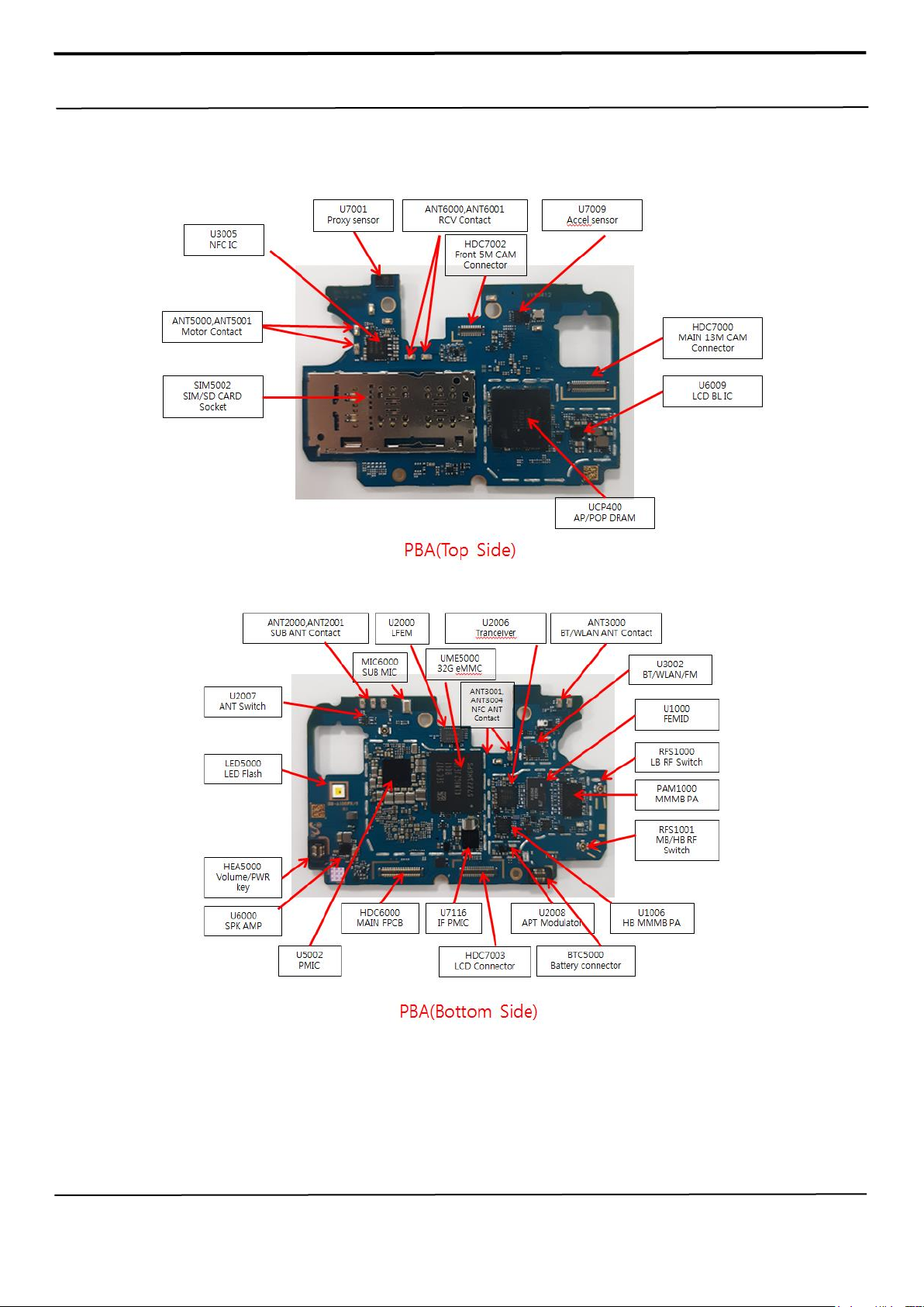
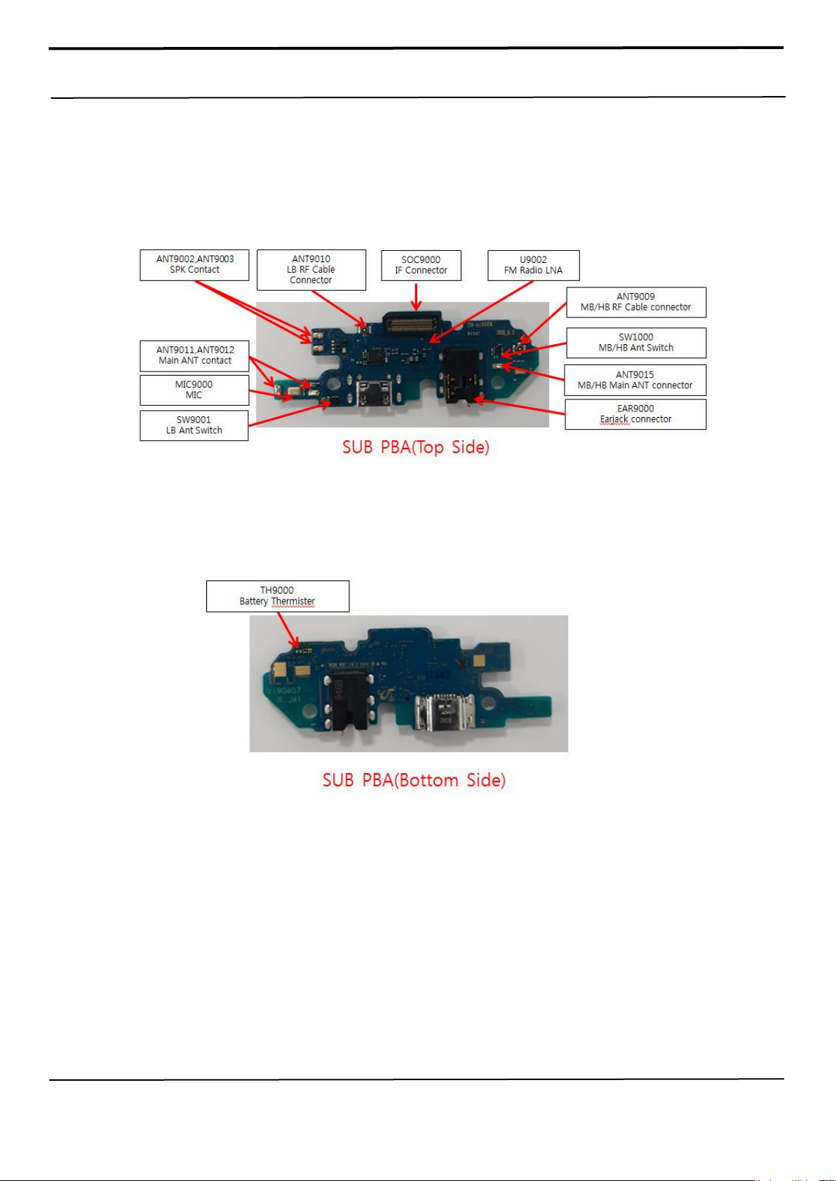
8. Level 3 Repair
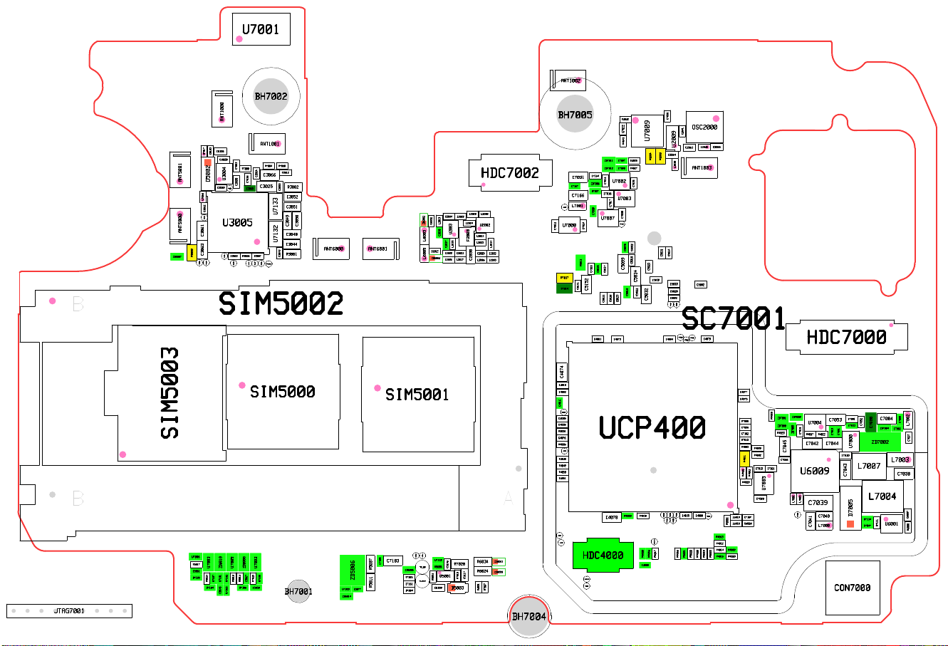
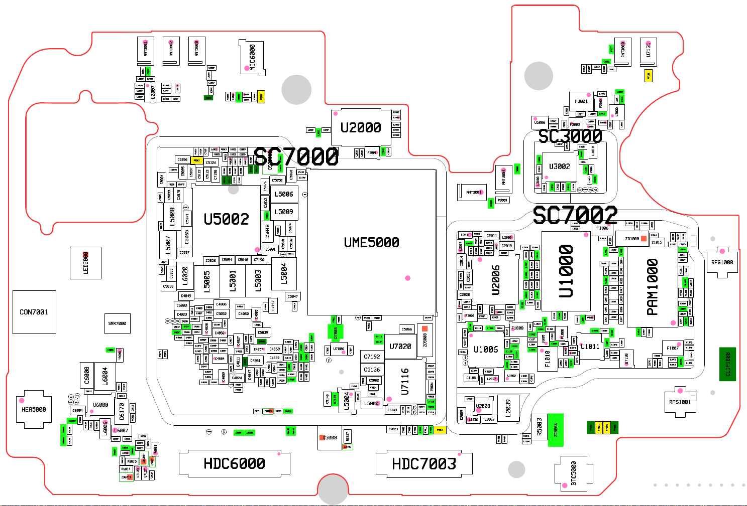
8-1. Components Layout
Confidential and proprietary-the contents in this service guide subject to change without prior notice
Distribution, transmission, or infringement of any content or data from this document without Samsung’s written authorization is strictly prohibited.
8. Level 3 Repair
Confidential and proprietary-the contents in this service guide subject to change without prior notice
Distribution, transmission, or infringement of any content or data from this document without Samsung’s written authorization is strictly prohibited.
S5M9150X01-L030
Transceiver
SAMSUNG
CONFIDENTIAL
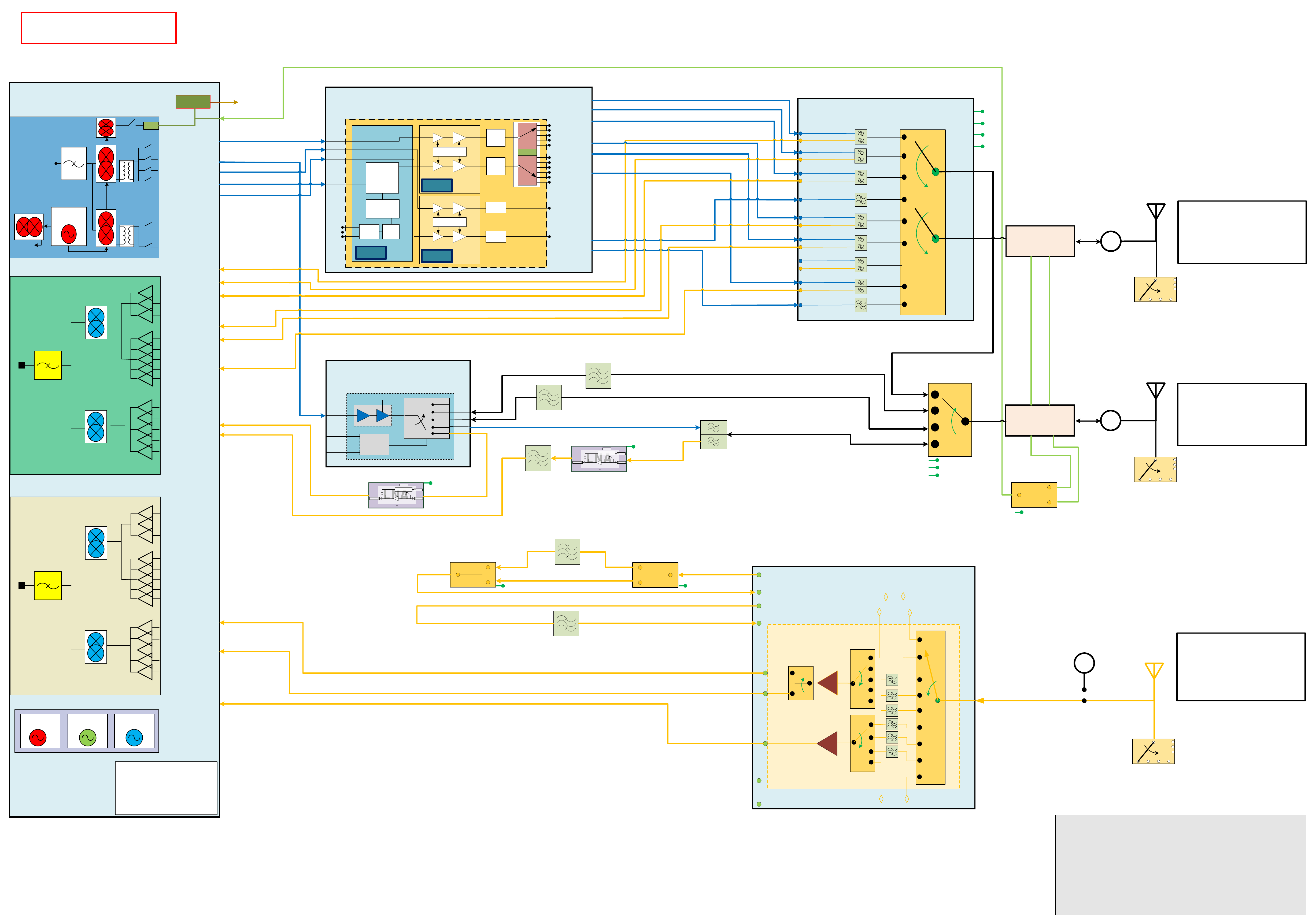
SM-A105FN/N(A10) RF BLOCK Diagram
2019.03.20
MAIN ANT 1
B5/8/20
EUR/KOR
2G : 850/900/1800/1900
3G : B1/2/5/8
4G : B1/2/3/5/7/8/20/38/40/41
SUB ANT
B1/2/3/5/7/8/20/38/40/
41
GNSS RF
PRX_HB1
PRX_HB2
PRX_HB3
PRX_MB1
PRX_MB2
PRX_MB5
PRX_MB3
PRX_MB4
PRX_TR_IN_B1
PRX_TR_IN_G1800_B3
TX_HMB3
TX_HMB4
TX_HMB2
TX_HMB1
TX_LB1
TX_LB2
TX_TR_OUT_1_2_3_4
TX_TR_OUT_GSMHB
TX_TR_OUT_GSMLB
PRX_LB4
PRX_LB3
PRX_LB1
PRX_LB2
PRX_LB5
DRX_MB1
DRX_MB2
DRX_MB3
DRX_MB4
DRX_HB1
DRX_HB2
QM13124A
ANT S/W
VIO
SCLK
TXLOTXLO_2G
PDET_OUT
PWDET
SDATA
20449-001E
RF Switch
VDD
CTRL1
CTRL2
TX_PA_OUT_B1
TX_PA_OUT_B3
TR_PDET_IN
LDJ18829M28DG014
Coupler
COUPLE
_FWD
BGSA14GN10-1
ANT S/W
LMSWKQGS-J79
Femid
VDD
VIO
SCLK
SDATA
B3
B5
B8
B12/17
B20
2G H Tx
2G L Tx
B5 Rx
B5 Tx
B8 Rx
B8 Tx
B12/17 Rx
B12/17 Tx
B20 Rx
B20 Tx
2G H Tx
2G L Tx
LB
SKY77656-11
MMMB_PA
RFOUT_B1
RFOUT_B3
RFOUT_B4
RFOUT_B8
RFOUT_B12/17
RFOUT_B20
GSM_HB
GSM_LB
RFOUT_B2
20449-001E
RF Switch
ANT
SFMLFU0H001
LFEM
RF_Low OUT
RF_High OUT
RF_Mid OUT
AUX
LB_In
AUX
LB_Out
AUX
MB_Out
AUX
HB_Out
AUX
MB_In
AUX
HB_In
B1/4
B3
B7
B5
B8
B20
B12/17/28
B2
B38/40/41
DRX_TR_IN_HB
DRX_TR_IN_MB
DRX_TR_IN_LB
MXD8621
SPDT
SAFFB2G35AA0F3K
DRX_SW_CTL1
AUX
HB_Out
MXD8621
SPDT
B38/41
B40
B38/40/41
DRX_SW_CTL0
SKY77786-11
HB MMMB
PA
PA & Switch
Control
RF IN
T/R
Switch
VCC
VBATT
VIO
SDATA
SCLK
RXTD2
HBTD2
HBTD1
HBFD1
RXTD1
RFOUT_B5
SFDG93AQ902
B834 7
TRX_B38_41
TRX_B40
MAIN ANT 2
B1/2/3/7/38/40/41
20449-001E
RF Switch
LDJ18829M28DG014
Coupler
ANT
MXD8642
SP4T
HB_SW_SEL0
HB_SW_SEL1
VDD
PRX_TR_IN_B38_40_41
SAYEY2G53BD0F3K
B7 Duplexder
LNA
MXD8921HS
B7 LNA
BIAS/CONTROL
VCC
CTRL
RF_INRF_OU T
PRX_LNA_EN_B7
SAFFB2G65AA0F0A
TRX_B7
PRX_TR_IN_B7
TX_PA_OUT_B2
PRX_TR_IN_G1900_B2
AUX
HB_In
AUX
MB_Out
AUX
MB_In
SAFFB1G96AB0F0A
B2
AUX
LB_Out
AUX
LB_In
B2
B2 Tx
LNA
MXD8921HS
B38/40/41 LNA
BIAS/CONTROL
VCC
CTRL
RF_INRF_OU T
PRX_LNA_EN_B38_40_41
COUPLE
_REV
MXD8621
SPDT
RST_SW
CPL_FWD
CPL_REV
DRX_HB3
B1
B1 Tx
B1 Rx
B2 Rx
B3 Tx
B3 Rx
PRX_TR_IN_B20
PRX_TR_IN_EGSM_B8
PRX_TR_IN_B5_G850
TX_TR_OUT_B7_38_40_41
TX_PA_OUT_GSMHB
TX_PA_OUT_GSMLB
TX_PA_OUT_B5
TX_PA_OUT_B8
TX_PA_OUT_B20
DRX_MB5
DRX_LB1
DRX_LB2
DRX_LB3
DRX_LB4
DRX_LB5
TX ABB
TX PORTs
TX HMB1
TX LB2
TX LB1
TX HMB2
TX HMB3
TX HMB4
TX ABB In
TX LO 2G/3G/4G
HB,MB,LB
To RX ABB out
RXLO
PRX ABB
PRX PORTs
RXLO
TXLO
TXLO_2G
PRX HB1
PRX HB2
PRX MB1
PRX MB4
PRX MB5
PRX LB1
PRX LB2
PRX LB3
PRX LB4
PRX LB5
PRX HB3
PRX MB3
PRX MB2
HB LNA
MB LNA
LB LNA
RXLO
TXLO
TXLO_2G
PRX
OUTPUT
DRX ABB
DRX PORTs
RXLO
TXLO
TXLO_2G
DRX HB1
DRX HB2
DRX MB1
DRX MB4
DRX MB5
DRX LB1
DRX LB2
DRX LB3
DRX LB4
DRX LB5
DRX HB3
DRX MB3
DRX MB2
HB LNA
MB LNA
LB LNA
RXLO
TXLO
TXLO_2G
DRX
OUTPUT
TX_TR_OUT_B5_8_12_17_20_28
SP3T
Bias &
Control
Circuit
Voltage
Regulat
or
MIPI
Decorder
UMTS PA
Bias circuit
CMOS IC
GSM PA
Bias circuit
WB
OMN
(MB)
WB
OMN
(LB)
OMN
OMN
SW
VIO
SCLK
RFOUT_GSM_HB
RFOUT_GSM_LB
MB
QM13124A
ANT S/W
VIO
SCLK
SDATA
TRX_MB
JTAG7001
ANT1000
C5106
C5103
U7017
C3028
U3004
D5002
TP_3005
C3060
U7016
C3062
TP_NFC_EN
U3005
ANT5000 ANT5001
C3061
C3063
R5009
C3022
ZD5007
TP_3004
TP_NFC_IRQ
TP_NFC_3000
TP_NFC_CLK_REQ
SIM5002
SIM5003
U7086
R5017
U7083
U7085
ZD6010
C5061
U7105
R5016
R5024
U7101
U7102U7103
U7107
U7104
C5049
U7001
BH7002
ANT1001
R7004
R7030
C7003
R7000
C3064
C3066
C7036
C3035
C3025
C3065
R3006 R3007
TP_FM_SPDY
TP_3006
TP_3007
TP_NFC_FIRM
SIM5000
U7092
ZD6006
C5067
R5014
R7029
U7108
C5058
U7106
R3012
R3002
C3053
C3052
C3051
U7133
C3049
C3048
U7132
C3044
R3001
C3043
BH7001
C3050
ANT6000 ANT6001
ANT1002
BH7005
HDC7002
L2018
L2020
C2034
L2022
L2019
ZD6002
C6032
L2024
U2002
U2003
C2038
L6003L6005
C6012
ZD6004
L2021
F2000
L2023
L2015
C2037
C2033
C2036
L2014
C2031
C2029
C2032
C2030
L2017
C2035
L2016
SIM5001
U7125
U7126
C7183
C7185
R5007
ZD5006
R5011
C5077
U7100
ZD5014
U7113
C5146
R5055
TP_UB
ZD5005
Q5001
R7026
R5054
TP_UB7001
C7161
C5109
U7084
D5003
ZD6011
R6034
R7020
R6024
ZD6001
C5117
R7015
R4001
R7007
C7031
C7167
C7166
L7001
TP7002
U7008
C7012
R7017
R7014
C4074
C4018
C4082
C4016
TP_XGNSS_GPLL_ANA_EXT
C4035
C4005
R4004
C4076
R4005
TP2000
R4048
R4049
R4050
R4051
U7119
U7120
R4042
C7022
R4043
ZD7011
C7097
C7098
C7164
U7002
C7014
ZD7006
U7037
C7016
U7003
C7017
C7009
C7008
U7007
TP7003
C7024
C5078
R5012
C5141
C5152
C5099
C5045
C7203
C5017
C5026
C5029
C5021
C4081
C4073
UCP400
R4000
C4078
HDC4000
XCLKOUT_TP
TP5000
C7050
OSC2000
C2041
U7009
U2009
L2040
C2065
C2061
C2064
R2003
R2004
R4025
R4027
C5010
L2038
ANT1003
C7015
C6022
C5024
C5031
C5018
C5023
C5034
C5019
C5033
C5002
C5020
C5022
C5032
C5092
TP_4004
TP_XCP_RF_ON4000
SC7001
TP4000
TP4002
C4079
C4004
TP4001
C4077
C4075
R7005
C7096
C7182
R7013
R4003
R4030
R4032
R4011
C7013
R4002
TH4000
R4029
C7020
TP_EMMC4000
TP5009
TP5010
TP5012
C4015
R4010
R4046
R6028
C4000
C4080
TP5008
TP5015
TP_XRTC_XTO
R4016
R4021
R4047
R5020
R7028
C7187
L6019
R6006
C6023
L6018
R4013
R4012
R4014
R4019
R5019
R5022
R4015
R4020
C7021
U7005
R4018
ZD7003
ZD7001
ZD7000
ZD7005
C7018
R4023
C7045
C7046
U6009
L7005
L7006
TP7000
HDC7000
C7001
C7053
U7004
R4017
C7042
C7039
R4022
C7040
C7041
L7008
C7044
C7052
C7011
C7000
C7019
C7051
ZD7002
U7000
C7010
L7007
C7043
L7004
D7005
U7114
C7047
C7004
ZD7004
U7111
U6001
C7002
L7003
C7038
C7005
L7002
C7037
C6007
R6000
CON7000
BH7004
CON7001
HEA5000
ANT2002
L2033
C5075
C5030
C5055
L5008
L5007
C5063
C5003
C4023
TP5011
TP5016
C5012
C4092
C4064
ANT2000
C2008
L2008
C2009
R2000
C5120
C7195
R5015
C5096
R5013
C5124
C5095
C5097
C5122
C5123
C5073
C5070
TP5007
C5071
U5002
C5065
C5037
C5056
L6020
L5005
C4049
C4050
C4088
C4022
C4012
C4067
C4056
C5004
C4030
C4062
U7124
C4028
C4054
C4066
C4091
C5007
C5006
C4065
C5008
C4072
C4053
C4045
C4001
C4043
C4044
C4029
C4026
C4083
TP4003
HDC6000
MIC6000
C2006
L6011
C4068
C4090
R6031
C4010
C7198
C4058
C4084
C4086
C5052
R6013
C4089
C4087
C5054
C4059
TP_SPEEDY_PMIC
L6001
L6000
C6000
C6005
R6003
ZD6000
C6001
C6002 C6003
C6025
C6035
R6023
C5101
C5115
C5102
C5104
C6036
C6037
R6017
R6020
SC7000
OSC5000
C5116
U7123
C5100
C5107
C5108
C5114
C7199
C7200
C5076
C5059
C5013
C5048
C5081
C5040
C7196
L5001
L5003
C4051
C4008
C4060
C4093
C4085
C4006
C5039
C4038
C4070
C4046
C4017
C4027
C4055
C4094
C4011
C4025
C4024
TP_PMIC_AP4000
R4007
R4009
ZD6017
C4069
C4057
C4063
C4039
C4061
C4048
C4052
C5009
C4003
C4047
C4009
C4002
ZD6003
C6171
ZD6005
C5050
L5006
L5009
C5025
C7197
C4071
C4014
C4020
C5016
C4036
C5000
R6025
C5093 C5094
C5035
TP5013
C5011
L5004
C5047
C4042
C4037
C4013
C4098
C4033
C4100
R6016
R6030
C5060
C5074
C5036
C4007
F3001
C2002
L2003
C2010
C2007
L2009
C5142
C5143
TP5001
L2013
U2000
C2003
L2025
L2026
C2004
C2000
C2039
C2040
F2001
ANT3004
ANT3001
R3003
ZD3000
U5006
ZD3001
SC7002
R2001
L2011
C2011
L2000
C2001
C2005
C2018
UME5000
C4019
C4097
C4041
C4021
C4095
C5014
C4099
C4040
C4096
C4034
C4101
C4102
C5015
C4103
C4104
R6029
D5000
C7006
C5149
U7118
R5008
R7012
Q7000
U7006
TP5014
R5000R5001
R5002
U7112
C5147
C7007
U7020
C7192
C5136
C5062
C5083
C5131
C5134
C5148
C5110
U7109
L5000
U5004
R6027
ZD6016
C5041
C7023
C5066
U7116
U7121U7122
C7193
C5118
C7033
C7032
C7034
C5144
ZD5000
C5042
C5043
R5005
R5004
R5010
U7110
R5050
C5079
C5154C5155
C7035
R7011
U7039
C2024
L2007
L2010
C2014
C2015
C2046
C2023
U2001
C2027
C2028
C2013
L2006
C2012
F3002
L3004
C1116
L1052
C1117
C1106
TP1000TP1001
C1108
C1105
C2062
C2059
R7010
L2036
C2016
L2001
L2004
C2017
L3005
C3017
C1114
U1006
C1098
L2037
C1099
U2008
C2063
C2019
L2002
C2020
U2006
C2021
C2026
L2012
C2022
C2025
C2045
C1124C1126
C1127
C1142
C1118
L1053
L1030
U1002
L2039
R4037
R4038
F1008
L1063
C1143
C1060
L1010
C1140
L1068
L1008
C1000
L1026
L1057
L1025
L1036
L1023
C1045
L1018
L6021
L1060
C1032
L1034
L1033
C1052
C1137
L1064
L1066
C1119
L1035
C1046
C1036
C5046
C7194
C3029
L3011
C5127
F3003
C3030
R5006
SC3000
L3012
C3007
L3010
C3008
C3001
L3008
C3020
C1024
L1027
L1014
C1044
L1061
C1021
C1128
C1056
U1005
R5003
U3002
C1139
C1009
F1010
C3009
C3031
C3024
R3000
C3026
C3021
C3023
TP_3002
L1013
C1031
U1000
C1038
C1039
C1066
R1003
F1000
C1029
C1079
C1131
C1073
U1011
U1003
L1032
C1071
L1019
L1062
C1130
ZD5004
HDC7003
BTC5000
ANT2001
C2054
C2055
C2056
L2032
L2034L2035
C2057
C2058
U2007
C2060
C2066 C2067
C5084
C5085
C5119
C5027
LED5000
C5028
C5038
SMR7000
C5005
VR6001
C6008
L6004
C7202
U6000
R4024
R6001
C6014
C6013
C6170
L6006
L6007
C6009
R6037
C6010
L6002
R6032
R6014
R6038
C6015
C6033
R6015
C7169
ZD6019
C6011
TP_AMP_I2C_DI
TP_AMP_I2S_DO
TP_AMP_I2S_BCLK
TP_AMP_I2S_WS
C6004
ZD5003
R5021
R4026
C5125C5126
ZD5001ZD5002
TP5006
C5129
R5023
R6019
C6024
R6036
R6022
R6018
ZD6014
U7093
U7127
U7128
C6029
U7137
C3012
C3013
C3027
L3007
L3009
C3014
L3002
C3006
L3001
F3000
C3005
C3011
U3000
C3000
L3000
C3015
L3006
ANT3000
U7136
L3003
U7131
U7138
C3010
C3003
C3004
C3018
C3019
TP_3003
TP_3000TP_3001
C1006
L1004
L1006
F1006
C1010
L1001
C1005
C1041
C1023
C1018
C1064
C1051
TH1000
L1024
C1054
C1028
C1030
C1012
R1000
L1015
L1000
C1004
L1002
C1040
L1016
L1009
C1022
L1005
C1017
L1028
C1061
L1029
L1022
C1047 C1050
C1033
C1067
C1077
C1076
C1120
L1055
L1054
C1015
PAM1000
C1007
C1016
C1008
U7130
C1070
C1014
ZD1000
C1034
C1035
C1037
C1025
L1017
C1026
L1011
C1027
C1011
U7129
L1003
C1003
C1020
L1007
F1007
R1005
C1072
ZD1001
R1001
R1006
R1011
RFS1000
C1092
L1012
ZD1002
C1102
R1010
C1001 C1002
C1013
C1019
C1075
C1078
L1045
L1049
CLIP1000
RFS1001
R7009
R7018
R7001
R7016
8. Level 3 Repair
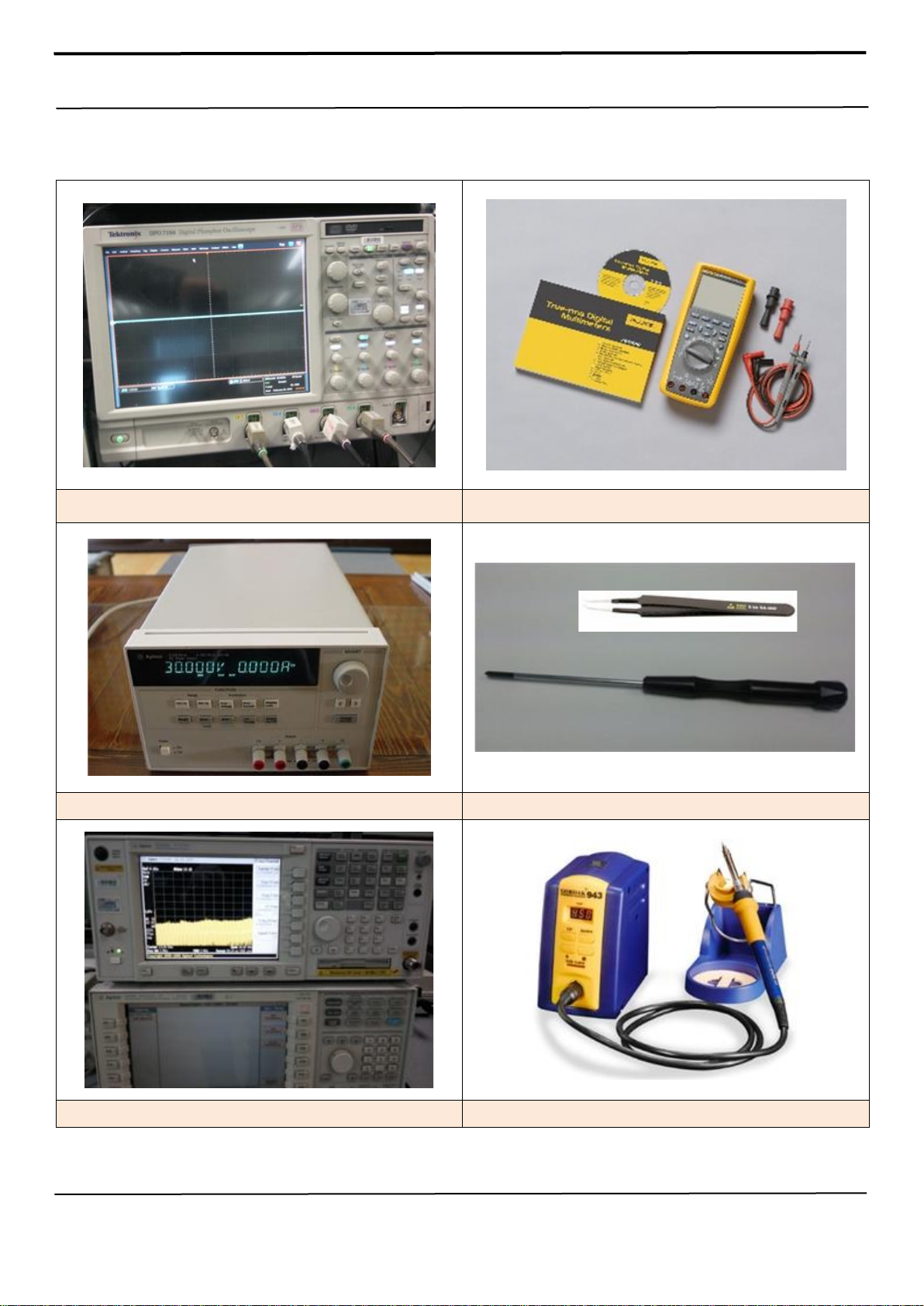
Oscilloscope
Digital Multimeter
Power Supply
+ driver, ESD Safe Tweezer
8960 & Spectrum Analyzer
Soldering iron
8-3. Flow chart of Troubleshooting.
Confidential and proprietary-the contents in this service guide subject to change without prior notice
Distribution, transmission, or infringement of any content or data from this document without Samsung’s written authorization is strictly prohibited.
8. Level 3 Repair
Mobile phone does not power on.
Yes
No
Charging the battery by TA.
If its voltage level is extremely low
(under 3.0V),
Change the battery.
END
Yes
Sound or Vibration is ok?
Yes
Change the FRONT-LCD ASSY
No
Check the voltage level at
R5021 while pressing power
key. Is the voltage high?
No
Replace the Power / Volume key FPCB
Yes
No
Check the output voltage of U5001
L5006 > 2.0V, L5005 > 1.35V, C4000 > 0.8V
C5030 > 0.85V, C5029 > 0.85V, L5003 > 0.8V
L5002 > 0.8V, L5004 > 0.8V, C4059 > 0.8V
C5007 > 1.0V, C5023 > 1.8V, C4043 > 0.9V
C4047 > 1.8V, C5025 > 1.2V, C5024 > 1.2V
C4051 > 3.0V, C4060 > 1.8V, C4062 > 1.2V
If the output voltage is not normal,
Change the U5001.
※ Each voltage level has ±10% margin.
Yes
No
Re-download Official Binary
If it is still problem, change the PBA
Yes
Check the Battery Voltage.
Is it more than 3.8V?
Check the Initial status
Current Binary : Samsung Official
System Status : Official
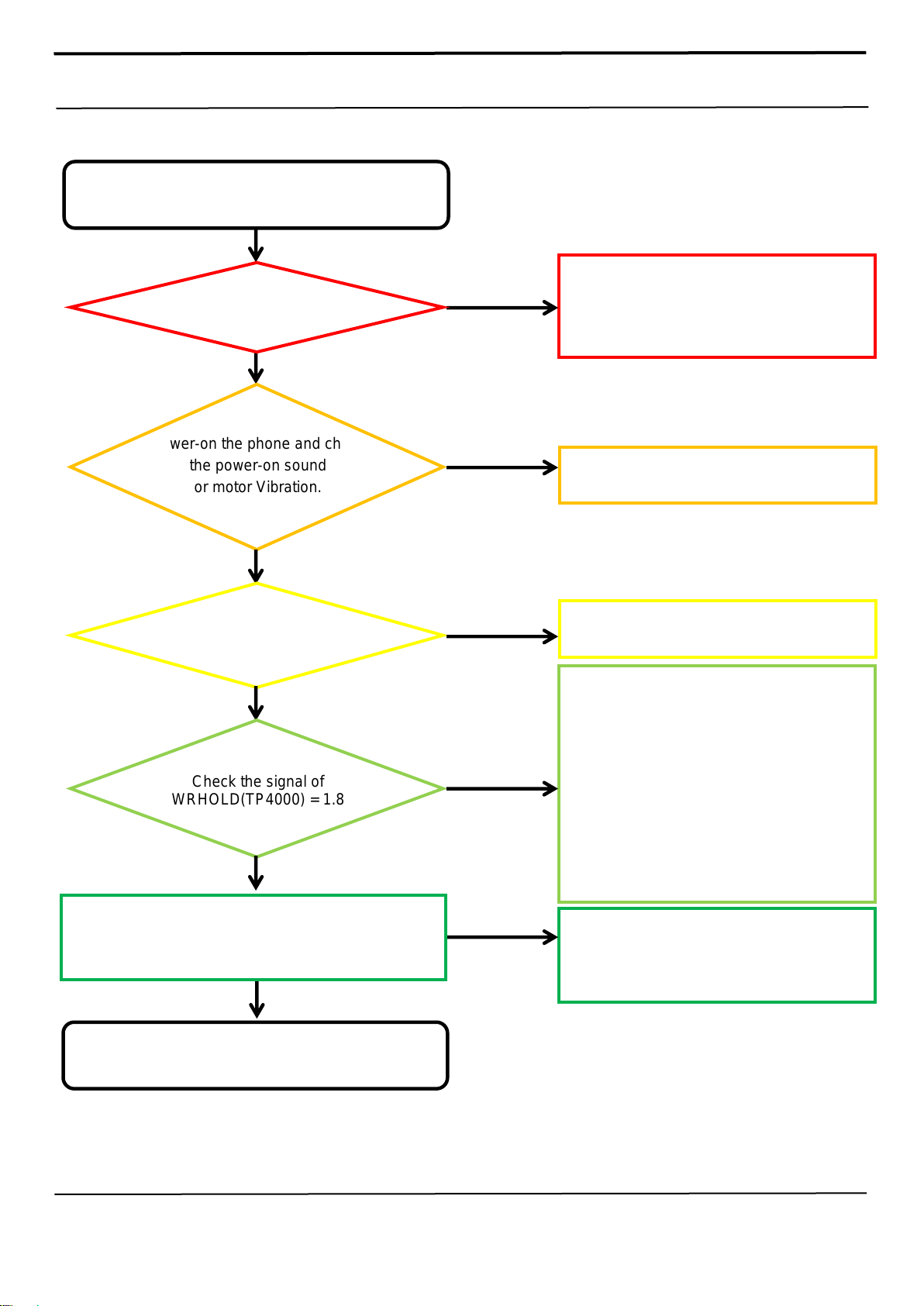
8-4-1. Power On
Power-on the phone and check
the power-on sound
or motor Vibration.
Check the signal of
PWRHOLD(TP4000) = 1.8V
Distribution, transmission, or infringement of any content or data from this document without Samsung’s written authorization is strictly prohibited.
Confidential and proprietary-the contents in this service guide subject to change without prior notice
8. Level 3 Repair
Initial Failure
Yes
Yes
END
Abnormal
Abnormal
Check the U5001 (Crack, open etc.)
Normal
Change UCP400 or UME5000
Abnormal
Change PBA
Check the Initial status
Current Binary : Samsung Official
System Status : Official
Re-download Official Binary
Normal
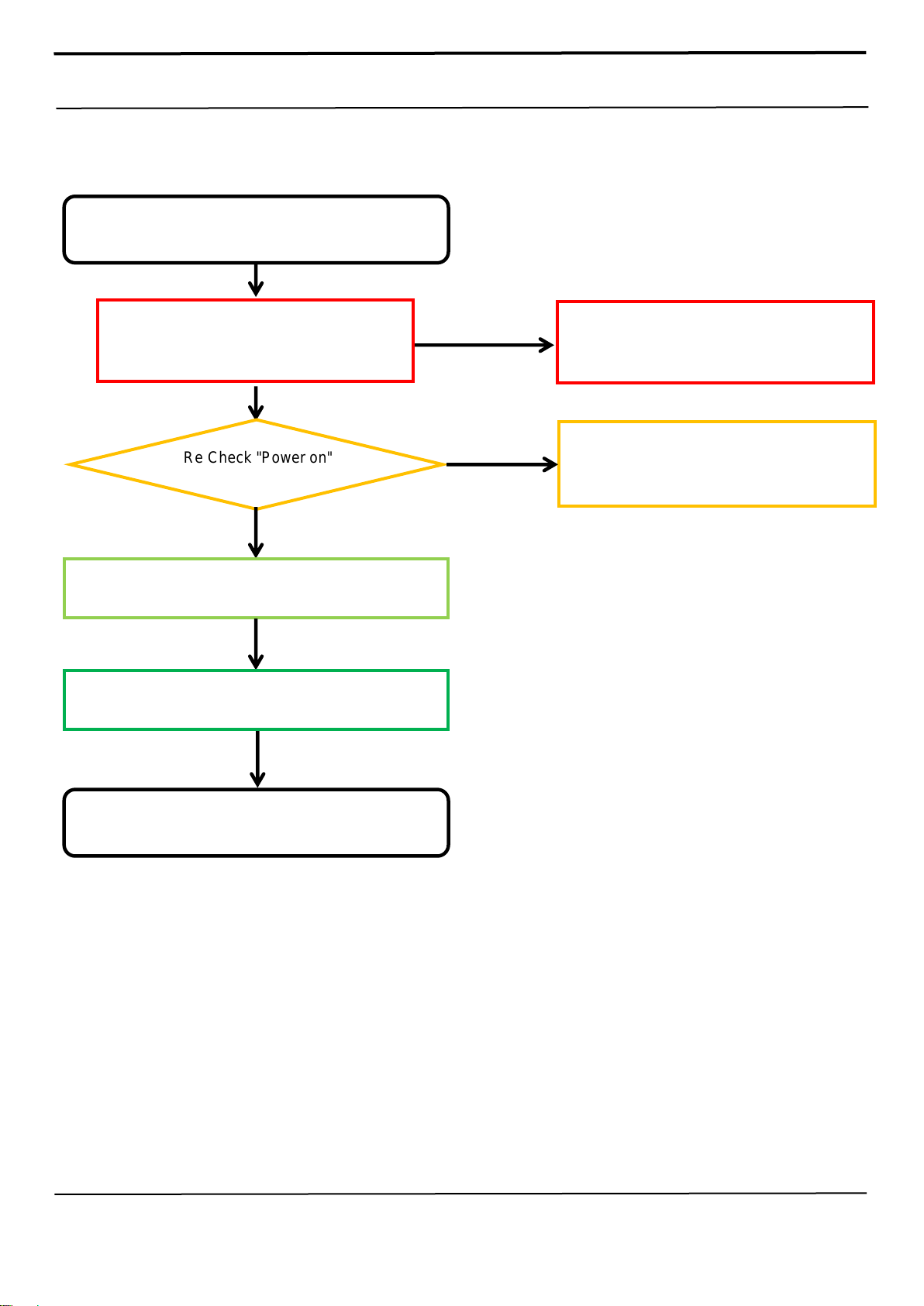
8-4-2. Initial
Re Check "Power on"
Trouble shooting process
Confidential and proprietary-the contents in this service guide subject to change without prior notice
Distribution, transmission, or infringement of any content or data from this document without Samsung’s written authorization is strictly prohibited.
8. Level 3 Repair
No service
Home screen → Phone
→ Keypad → *#1234#
→ check Phone version
Check status OK at coaxial Cable, SUB
PBA and
ANTENNA materials
If ANTs are OK, Please check
RFS1000,RFS1001, C1004, C1008,
L1008, C1014
Replace the TCX1000, C7175,
Yes
CP : M105FXXX
Check U5001 damaged.
CP : unknown
END
Check menu setting
Menu → applications → setting → connections →
mobile networks → network mode →
setting is auto connect?
Check the voltage.
VDD_1P8_CP = 1.8V ?
VRF_RX_1P2_LO = 1.2V ?
VRF_TX_1P2_LO = 1.2V ?
VRF_TRX_1P8 = 1.8V ?
VRF_TX2LO_1P8=1.8V ?
VRF_TX_1P2=1.2V ?
VRF_RX_1P2=1.2V ?
Check TCX1000, C7175,
R1004
Frequency = 26MHz
Replace U2013
No
Yes
No
Yes
Yes
8-4-3. No Service
Distribution, transmission, or infringement of any content or data from this document without Samsung’s written authorization is strictly prohibited.
Confidential and proprietary-the contents in this service guide subject to change without prior notice
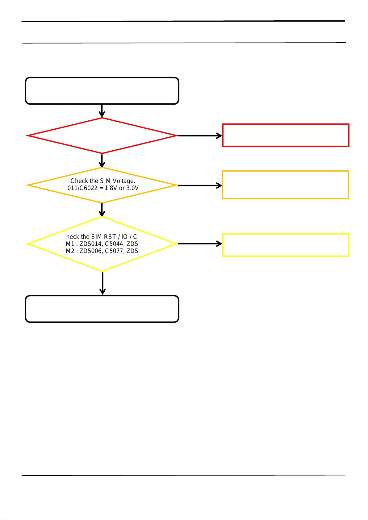
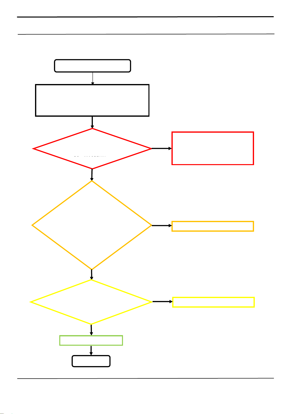
8. Level 3 Repair
Insert SIM card
Yes
Yes
END
C6011/C6022 = 1.8V or 3.0V?
No
Change to the new SIM card.
Is SIM socket ok?
Yes
No
Replace SIM socket
No
Yes
Check the UCP400 (Crack etc)
8-4-4. SIM Part
Check the SIM Voltage.
Check the SIM RST / IO / CLK.
(SIM1 : ZD5014, C5044, ZD5006)
(SIM2 : ZD5006, C5077, ZD5006)
Is signal ok?
Confidential and proprietary-the contents in this service guide subject to change without prior notice
Distribution, transmission, or infringement of any content or data from this document without Samsung’s written authorization is strictly prohibited.

8. Level 3 Repair
Insert T-Flash card
Yes
Yes
END
No
Change to the new T Flash card.
If it doesn`t still work T Flash card after
changing
the T FLASH, Check the U5005
(Crack etc)
Is T-Flash socket ok?
Yes
No
Replace T-Flash socket
No
Yes
Check the UCP400 (Crack etc)
8-4-5. T-Flash Part
Check the T-Flash Voltage.
C7183 = 3.0V?
Check the T-Flash
CMD/Data/CLK.
(R5016, R5017, R6006)
Is signal ok?
Distribution, transmission, or infringement of any content or data from this document without Samsung’s written authorization is strictly prohibited.
Confidential and proprietary-the contents in this service guide subject to change without prior notice

8. Level 3 Repair
Insert TA / USB
Yes
Yes
END
No
Check OVP IC (U5004)
Charging Sequence Start
VBUS_5V_CON (C5149) = 5V
Yes
No
Replace SUB PBA
No
Yes
Check the U5002 (Crack, short etc.)
8-4-6. Charging Part
VBUS_5V_OVP (C5110)=5V
Check the
Battery is Charging?
Confidential and proprietary-the contents in this service guide subject to change without prior notice
Distribution, transmission, or infringement of any content or data from this document without Samsung’s written authorization is strictly prohibited.

8. Level 3 Repair
OTG does not work
Yes
Yes
END
No
Check U5004
(crack, open, damaged, etc.)
Check the
VBUS_5V_OVP(L5000) = 5V
Yes
No
Check U5002
(crack, open, damaged, etc.)
No
Yes
Replace SUB PBA
8-4-7. OTG
VBUS_5V_CON(C5149) = 5V
Check the
Check OTG working ?
Confidential and proprietary-the contents in this service guide subject to change without prior notice
Distribution, transmission, or infringement of any content or data from this document without Samsung’s written authorization is strictly prohibited.
8. Level 3 Repair
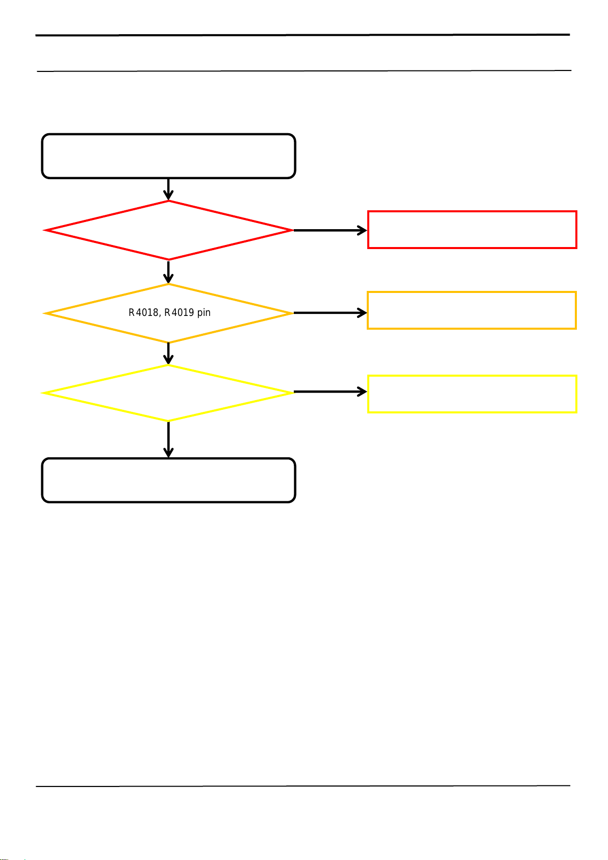
Accel Sensor does not work
Yes
Yes
END
Check Accel
(I2C is OK?)
No
Replace UCP400
Check the voltage
C7022, C7050 =1.8V
Yes
No
Replace U5001
(crack, open, etc.)
Abnormal
Yes
Replace U7009
8-4-8-1. Accel Sensor
R4018, R4019 pin
Check U7009
Confidential and proprietary-the contents in this service guide subject to change without prior notice
Distribution, transmission, or infringement of any content or data from this document without Samsung’s written authorization is strictly prohibited.
 Loading...