

Samsung SIP0P5WRS50 User Manual
SIP0P5WRS50
Samsung Semiconductor, Inc. SIP0P5WRS50 Module Datasheet
Samsung Confidential
Specifications in this document are tentative and subject to change.
Samsung’s ARTIK™ Module is a highly integrated module for
secure Internet of Things (IoT) devices that require Wi-Fi. It is
based on an ARM® Cortex® R4 core with on-chip memories,
an ARM® Cortex® M0+ core, a complete 2.4GHz Wi-Fi Phy,
MAC layer processing, a large complement of standard digital
buses including audio (I2S), and power management. The
module is packaged with additional external Flash memory, a
hardware Secure Element and a single integrated 2.4GHz
structural antenna.
The application processor is fully available for applications
since the Wi-Fi stack, through the MAC layer, is handled by a
co-processor. Aimed especially at power-sensitive devices
needing Wi-Fi, the SIP0P5WRS50 Module provides excellent
performance in a variety of environments, with a feature set
tailored specifically for IoT end nodes.
Top View (Image is preliminary and will change)
SIP0P5WRS50 Module Block Diagram
Processor
CPU
ARM® Cortex® R4, 32-bit
with 32KB I-Cache and
32KB D-Cache @ 320MHz
WLAN CPU
ARM Cortex M0+ @
320MHz
Memory
Embedded ROM
64KB
User Embedded RAM
1.25MB
128KB (Shared)
FLASH
8MB SPI FLASH on Module
Security
Secure Element
Secure point to point
authentication and data
transfer
Radio
WLAN
IEEE802.11™ b/g/n
2.4GHz radio
Power Management
Single Supply
Provides all power of the
SIP0P5WRS50 Module
using 3.3V
Interfaces
Digital I/O
UART, I2C, I2S, SPI, PWM
and GPIO
SAMSUNG ELECTRONICS RESERVES THE RIGHT TO CHANGE PRODUCTS, INFORMATION AND SPECIFICATIONS WITHOUT NOTICE.
Products and specifications discussed herein are for reference purposes only. All information discussed herein is provided on an "AS IS" basis, without warranties
of any kind. This document and all information discussed herein remain the sole and exclusive property of Samsung Electronics. No license of any patent,
copyright, mask work, trademark or any other intellectual property right is granted by one party to the other party under this document, by implication, estoppel
or other-wise. Samsung products are not intended for use in life support, critical care, medical, safety equipment, or similar applications where product failure
could result in loss of life or personal or physical harm, or any military or defense application, or any governmental procurement to which special terms or
provisions may apply. For updates or additional information about Samsung products, contact your nearest Samsung office. All brand names, trademarks and
registered trademarks belong to their respective owners.
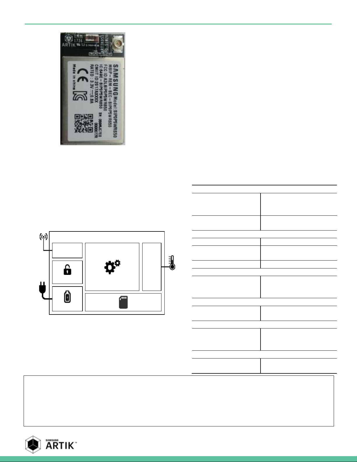
ARTIK 051 MODULE
RADIO
SECURITY
PROCESSOR
POWER MGT. MEMORY
INTERFACES
2

Samsung Semiconductor, Inc. SIP0P5WRS50 Module Datasheet
Samsung Confidential
Specifications in this document are tentative and subject to change.
TABLE OF CONTENTS
Table of Contents ................................................................................................................................................................... 3
List of Figures .......................................................................................................................................................................... 4
List of Tables ........................................................................................................................................................................... 4
Version History ...................................................................................................................................................................................... 5
SIP0P5WRS50 Module Block Diagram and Component Placement ................................................................................ 6
SIP0P5WRS50 Module Wi-Fi Interface ................................................................................................................................................ 6
SIP0P5WRS50 Module Memory ........................................................................................................................................................... 6
SIP0P5WRS50 Module Power Management Unit .............................................................................................................................. 7
SIP0P5WRS50 Module Security Subsystem ........................................................................................................................................ 7
SIP0P5WRS50 Module ADC Interface .................................................................................................................................................. 7
SIP0P5WRS50 Module UART Interface ................................................................................................................................................ 8
SIP0P5WRS50 Module GPIO Interface ................................................................................................................................................ 8
SIP0P5WRS50 INT Interface ................................................................................................................................................................. 8
SIP0P5WRS50 Module I2C Interface .................................................................................................................................................... 9
SIP0P5WRS50 Module SPI Interface.................................................................................................................................................... 9
SIP0P5WRS50 Module PWM Interface ................................................................................................................................................ 9
SIP0P5WRS50 Module I2S Interface .................................................................................................................................................... 9
SIP0P5WRS50 Module Processor System ........................................................................................................................................... 9
SIP0P5WRS50 Module Edge Connector ............................................................................................................................ 10
SIP0P5WRS50 Functional Interfaces .................................................................................................................................. 13
ADC Interface ....................................................................................................................................................................................... 13
Debug Interface ................................................................................................................................................................................... 13
GPIO Interface ..................................................................................................................................................................................... 13
I2C Interface ......................................................................................................................................................................................... 14
INT Interface ........................................................................................................................................................................................ 14
Power Interface ................................................................................................................................................................................... 14
PWM Interface ..................................................................................................................................................................................... 14
Reset Interface ..................................................................................................................................................................................... 15
SPI Interface ........................................................................................................................................................................................ 15
UART Interface ..................................................................................................................................................................................... 15
SIP0P5WRS50 Module GPIO Alternate Functions ............................................................................................................ 16
SIP0P5WRS50 Module Booting Sequence......................................................................................................................... 18
SIP0P5WRS50 Module Wi-Fi Antenna structure ............................................................................................................... 19
SIP0P5WRS50 Module Electrical Specifications ................................................................................................................ 19
Absolute Maximum Rating ................................................................................................................................................................. 20
DC Electrical Characteristics .............................................................................................................................................................. 20
DC Module Use Case Characteristics ................................................................................................................................................ 21
Power Supply Requirements .............................................................................................................................................................. 21
ESD Ratings .......................................................................................................................................................................................... 21
RF Electrical Characteristics ............................................................................................................................................................... 21
SIP0P5WRS50 Module Mechanical Specifications ........................................................................................................... 22
SIP0P5WRS50 Module FCC Certification ........................................................................................................................... 23
SIP0P5WRS50 Module Ordering Information ................................................................................................................... 24
Legal Information ................................................................................................................................................................. 25
3

Samsung Semiconductor, Inc. SIP0P5WRS50 Module Datasheet
Samsung Confidential
Specifications in this document are tentative and subject to change.
LIST OF FIGURES
Figure 1. SIP0P5WRS50 Module Block Diagram ................................................................................................................... 6
Figure 2. ADC LSB behavior .................................................................................................................................................... 8
Figure 3. SIP0P5WRS50 Module Edge Connector ............................................................................................................. 10
Figure 4. Booting and Reset Timing Relations ................................................................................................................... 18
Figure 5. RF Connector for Wi-Fi Antenna ............................................................ 오류! 책갈피가 정의되어 있지 않습니다.
Figure 6. SIP0P5WRS50 Module Mechanical Dimensions ................................................................................................ 22
LIST OF TABLES
Table 1. SIP0P5WRS50 Module Edge Connector Table Signal Descriptions .................................................................. 10
Table 2. ADC Interface .......................................................................................................................................................... 13
Table 3. Debug Interface ...................................................................................................................................................... 13
Table 4. GPIO Interface ......................................................................................................................................................... 13
Table 5. I2C Interface ............................................................................................................................................................. 14
Table 6. Interrupt Interface .................................................................................................................................................. 14
Table 7. PWM Interface......................................................................................................................................................... 14
Table 8. Reset Interface ........................................................................................................................................................ 15
Table 9. SPI Interface ............................................................................................................................................................ 15
Table 10. UART Interface ...................................................................................................................................................... 15
Table 11. Alternate functions of the SIP0P5WRS50 Module............................................................................................ 16
Table 12. Absolute Maximum Ratings ................................................................................................................................ 20
Table 13. I/O DC Electrical Characteristics(PAD:5,6,14-26,29-31,33-42,44-73, IO) ........................................................ 20
Table 14. I/O DC Electrical Characteristics(PAD:2-5, ADC) ............................................................................................... 20
Table 15. Recommended Operating Conditions ............................................................................................................... 21
Table 16. I/O Drive Strength ................................................................................................................................................ 21
Table 17. ESD Ratings ........................................................................................................................................................... 21
4
Samsung Semiconductor, Inc. SIP0P5WRS50 Module Datasheet
Samsung Confidential
Specifications in this document are tentative and subject to change.
Revision
Date
Description
Maturity
V0.1
07/26/2017
First Draft SIP0P5WRS50 Module Datasheet
Pre Alpha
V0.11
8/24/2017
Add legal information
Pre Alpha
V0.12
8/30/2017
Fix typos
Pre Alpha
VERSION HISTORY
5
Samsung Semiconductor, Inc. SIP0P5WRS50 Module Datasheet
Samsung Confidential
Specifications in this document are tentative and subject to change.
User Domain
UART
PWM
SPI
GPIO
DEBUG
I2S
PROCESSOR
CORTEX R4
32KB I$
32KB D$
BRIDGE
CRYPTO
ACCELERATOR
DMA
TCM
RAM/ ROM
32KB/32KB
BRIDGE
WLAN CO-PROCESSOR
32KB I-Cache, 16KB D-Cache
96KB SRAM
80 2.11 MAC
WLAN DOMAIN
2.4GHz
RADIO
RTC
PMU
PLL
LDO
BRIDGE
80 2.11 PHY
I2C
1.25MB SRAM
128KB SRAM
64KB ROM
UART <-> USB
PMIC
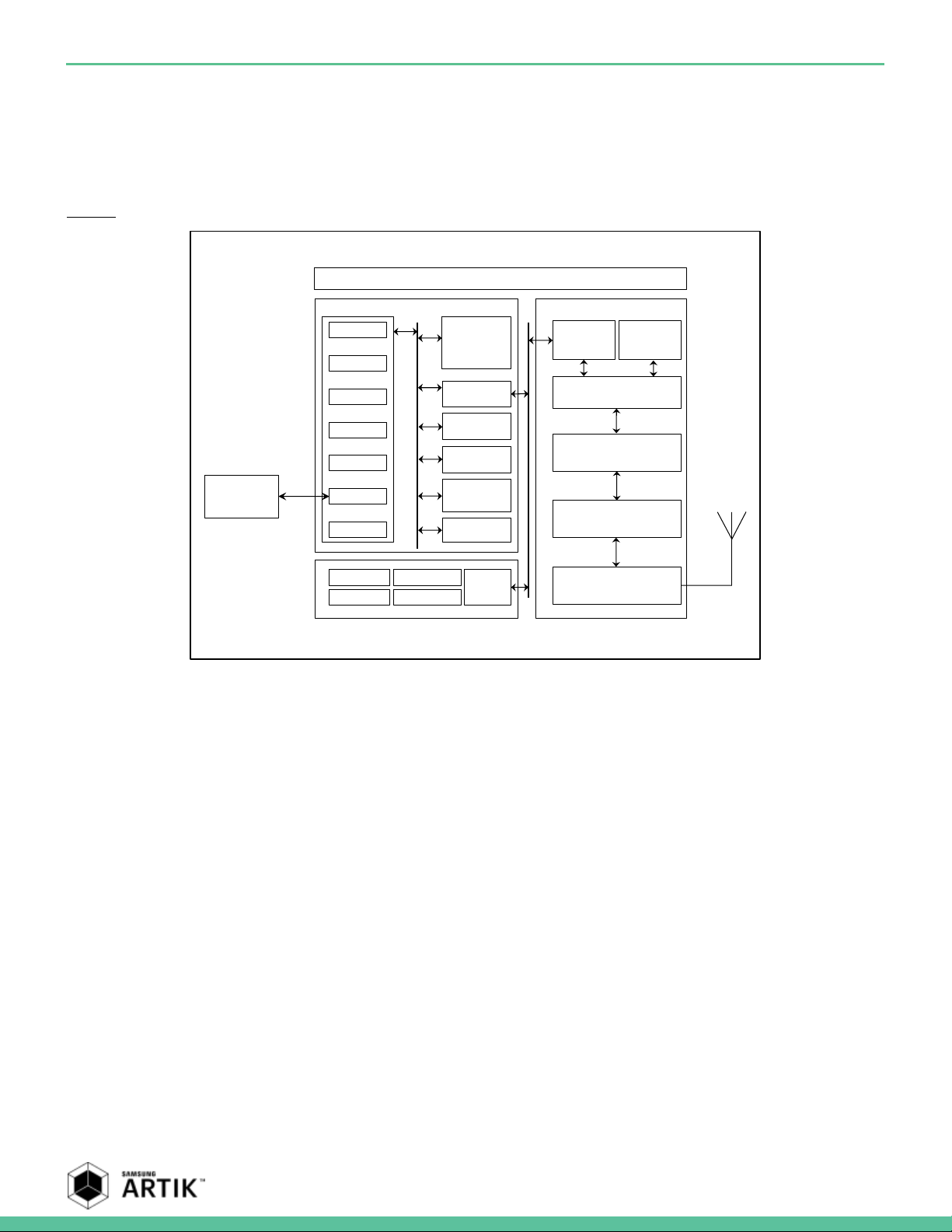
SIP0P5WRS50 MODULE BLOCK DIAGRAM AND
COMPONENT PLACEMENT
Figure 1 shows the functional Block Diagram of the SIP0P5WRS50 Module.
Figure 1. SIP0P5WRS50 Module Block Diagram
SIP0P5WRS50 MODULE WI-FI INTERFACE
The SIP0P5WRS50 Module has an 802.11b/g/n Wi-Fi subsystem. The most important hardware features of the Wi-Fi system
are:
802.11b/g/n support @ 2.4GHz
20MHz SISO (802.11n)
UDP throughput up to 50Mbps
WPA/WPA2/WAPI with WEP/TKIP implemented in software
Dedicated Wi-Fi Processor Sub System
o ARM
o Operating frequency of 320MHz
o 32KB I-Cache
®
Cortex® R4 Processor @ 480 MHz
o 16KB D-Cache
o Tightly Coupled Memory (32KB Code Memory/32KB Data Memory)
o SRAM 96KB
SIP0P5WRS50 MODULE MEMORY
The SIP0P5WRS50 Module has a memory subsystem with the following hardware features:
Internal RAM for secure boot, secure OS and general purpose operations.
o 1280KB dedicated RAM
6

Samsung Semiconductor, Inc. SIP0P5WRS50 Module Datasheet
Samsung Confidential
Specifications in this document are tentative and subject to change.
o 128KB shared RAM
Internal ROM for secure boot and secure OS operations.
o 64KB dedicated ROM
SIP0P5WRS50 MODULE POWER MANAGEMENT UNIT
The SIP0P5WRS50 Module has one universal power management unit that controls the state of power on the SIP0P5WRS50
Module. The most important features of the PMU are:
Fine granular power control
o Through the use of power domains
System level power control
o Deep stop mode
o Sleep power mode
Power savings techniques
o Frequency scaling
o Clock gating
o Power gating
SIP0P5WRS50 MODULE SECURITY SUBSYSTEM
The SIP0P5WRS50 Module has a dedicated security subsystem to ensure a secure end to end operation in any IoT
environment. The most important features of the SIP0P5WRS50 Module security subsystem are:
Isolated Execution Environment
o Isolated Cortex-M0 processor
o 8KB ROM for secure booting
o 32KB secure SRAM
o Dedicated secure DMA channel for secure backup/restore of SRAM content
o Secure Mailbox (68x32b wide) for secure communication
o Isolated key support
Backup encryption key 256-bits
SSS root private key 521-bits
Storage key 256-bits
Symmetric key engines
o Secure AES
o Secure DES/Triple-DES
Stream cipher engine
o ARC4 engine
Various Hash engines
o SHA-1/SHA2-256/ SHA2-384/ SHA2-512/MD5 HMAC
Asymmetric key engines
o PKA (Public Key Accelerator) engine
PRNG (Pseudo Random Number Generator)
DTRNG (Digital True RNG)
Secure timer
Secure key manager
DMA Support, Descriptor DMA
Block ciphers + hashing
Retention reset scheme
SIP0P5WRS50 MODULE ADC INTERFACE
The SIP0P5WRS50 Module has one 4-channel selectable analog to digital converter. The most important hardware features of
the A/D interface are:
Programmable 4-channel selection
7
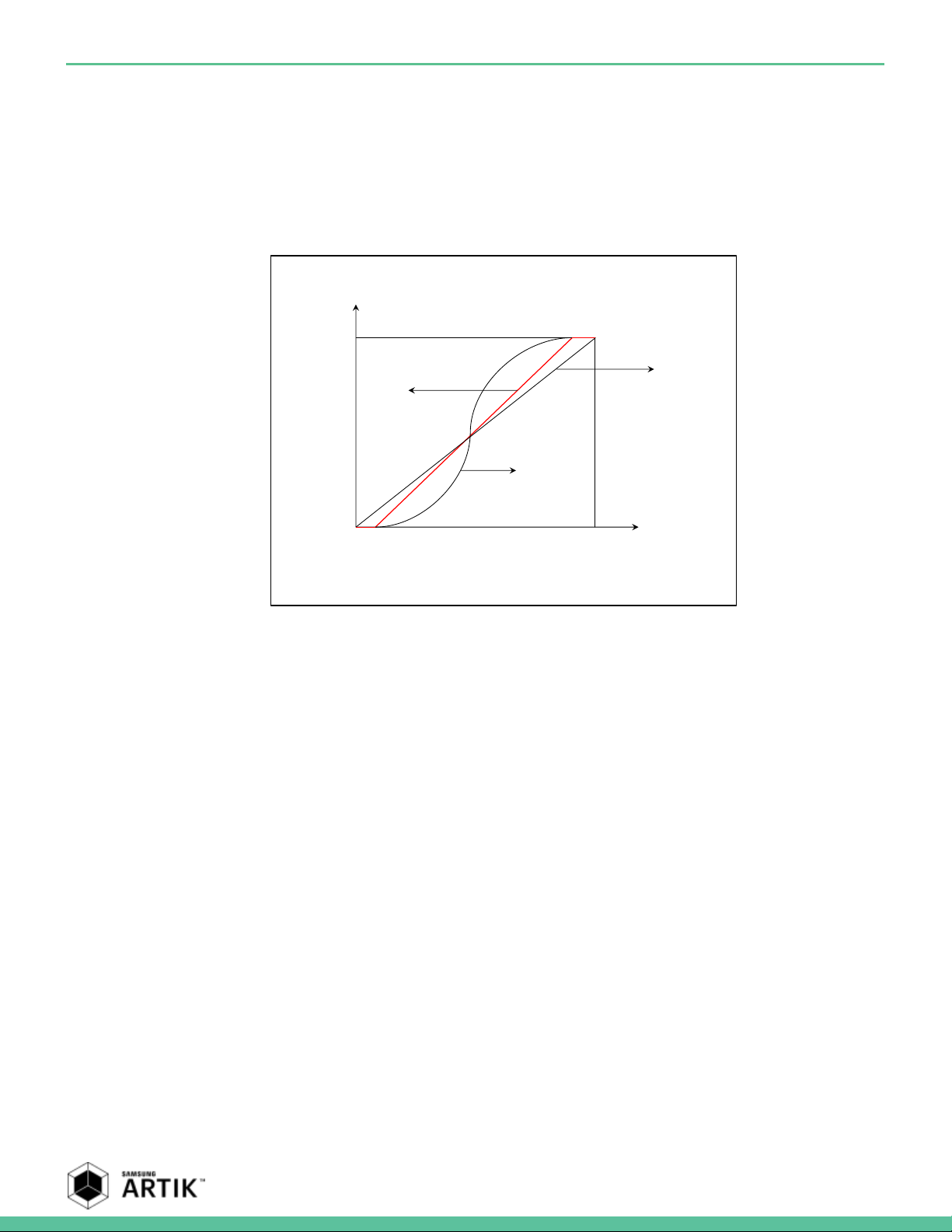
Samsung Semiconductor, Inc. SIP0P5WRS50 Module Datasheet
Samsung Confidential
Specifications in this document are tentative and subject to change.
Result (LSB)
Analog in (V)
Top
offset
Bottom
offset
Real
value
Ideal
value
Ideal value
with offset
Main ADC clock at 6.5MHz
Conversion clock ADC at 1.08MHz
Support for selectable conversion mode: 1, 2, 4, 8, 16, 32, 64
Differential non-linearity error ±2 LSB
Integral non-linearity error ±6 LSB
Top offset error ±10 LSB
Bottom offset error ±10 LSB
Figure 2 depicts the dynamic behavior between input voltage on the ADC and resulted LSB value in the ADC register.
Figure 2. ADC LSB behavior
SIP0P5WRS50 MODULE UART INTERFACE
By default the SIP0P5WRS50 Module has three, 2-pin UART interfaces. Using GPIOs that are currently used for other
functionality you can potentially create two 4-pin UART interfaces. The most important hardware features of the UART
interface is:
The UART can be operated in DMA or interrupt-based mode
Support for 5-bit, 6-bit, 7-bit or 8-bit serial data transmit and receive
Programmable baud rate
One or two stop bit insertion
SIP0P5WRS50 MODULE GPIO INTERFACE
The SIP0P5WRS50 Module has an extensive general purpose Input/Output interface. The most important features of the
SIP0P5WRS50 Module GPIO interface are:
Support for 62 multi-function input output ports.
Support for 27 dedicated GPIO ports
Control of 16 external interrupts
SIP0P5WRS50 INT INTERFACE
The SIP0P5WRS50 Module is equipped with an interrupt controller. The most important features of the SIP0P5WRS50 Module
Interrupt Interface are:
Enable, disable and generate interrupts from peripheral sources
Software generated interrupts
Interrupt masking and prioritization
8
 Loading...