

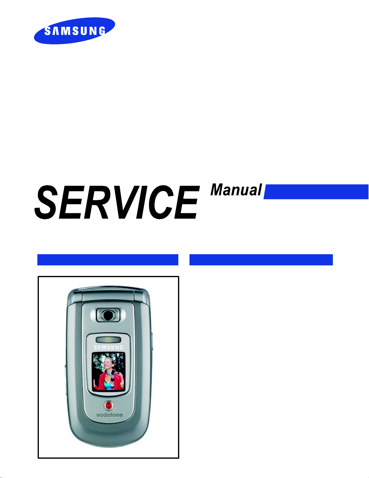
UMTS TELEPHONE
SGH-ZV30
UMTS TELEPHONE
CONTENTS
1. Specification
2. Circuit Description
3. Exploded Views and Parts List
4. Electrical Parts List
5. Block Diagrams
6. PCB Diagrams
7. Flow Chart of Troubleshooting
This Service Manual is a property of Samsung Electronics Co.,Ltd.
Any unauthorized use of Manual can be punished under applicable
International and/or domestic law.
ⓒ
Samsung Electronics Co.,Ltd. September. 2005
Printed in Korea.
Code No.: GH68-08450A
BASIC.
1. Specification
1-1. GSM General Specification
EGSM 900 DCS1800 PCS1900 W-CDMA
Freq.
Band[MHz]
Uplink/Downlink
ARFCN range
Tx/Rx spacing 45MHz 95MHz 80MHz 190MHz
Mod. Bit rate/
Bit Period
Time Slot
Period/Frame
Period
Modulation 0.3GMSK 0.3GMSK 0.3GMSK
MS Power 33dBm~5dBm 30dBm~0dBm 30dBm~0dBm 24dBm ~ - 50dBm
Power Class
880~915
925~960
0~124 &
975~1023
270.833kbps
3.692us
576.9us
4.615ms
4
(max +33dBm)1(max +30dBm)1(max +30dBm)
1710~1785
1805~1880
512~885 512~810
270.833kbps
3.692us
576.9us
4.615ms
1850~1910
1930~1990
270.833kbps
3.692us
576.9us
4.615ms
1920~1980
2110~2170
UL:9612~9888
DL:10562~10838
3.84Mcps
Frame length : 10ms
Slot length : 0.667ms
QPSK
HQPSK
3
(max +24dBm)
Sensitivity -102dBm -100dBm - 100dBm -106.7dBm
TDMA Mux 8 8 8
Cell Radius 35Km 2Km 2Km 2Km
1-1
SAMSUNG Proprietary-Contents may change without notice
This Document can not be used without Samsung's authorization
Specification
1-2. GSM TX power class
TX Power
control level
533±2dBm
631±2dBm
729±2dBm
827±2dBm
925±2dBm
10 23±2 dBm
11 21±2 dBm
GSM900
TX Power
control level
030±3dBm
128±3dBm
226±3dBm
324±3dBm
422±3dBm
520±3dBm
618±3dBm
DCS1800
TX Power
control level
030±3dBm
128±3dBm
226±3dBm
324±3dBm
422±3dBm
520±3dBm
618±3dBm
PCS1900
12 19±2 dBm
13 17±2 dBm
14 15±2 dBm
15 13±2 dBm
16 11±3 dBm
17 9±3dBm
18 7±3 dBm
19 5±3 dBm
716±3dBm
814±3dBm
912±4dBm
10 10±4 dBm
11 8±4dBm
12 6±4 dBm
13 4±4 dBm
14 2±5 dBm
716±3dBm
814±3dBm
912±4dBm
10 10±4 dBm
11 8±4dBm
12 6±4 dBm
13 4±4 dBm
14 2±5 dBm
15 0±5 dBm
1-2
15 0±5 dBm
SAMSUNG Proprietary-Contents may change without notice
This Document can not be used without Samsung's authorization

2. Circuit Description
2-1. SGH-ZV30 RF Circuit Description
- Antenna Switch Module (U106)
The antenna switch module allows multiple operating bands and modes to share the same antenna. A common
antenna connects to one of five paths: 1) UMTS-2100 Rx/Tx, 2) EGSM-900 Rx, 3) EGSM-900 Tx, 4) DCS-1800
Rx, and 5) DCS-1800 Tx. 6) PCS-1900 Tx, 7) PCS-1900 Rx, UMTS operation requires simultaneous reception and
transmission.
-Filter
To convert Electromagnetic Field Wave to Acoustic Wave and then pass the specific frequency band.
- GSM Rx FILTER (F100) : For filtering the frequency band between 925 ~ 960 MHz.
- DCS Rx FILTER (F101) : For filtering the frequency band 1805 and 1880 MHz.
- PCS Rx FILTER (F102) : For filtering the frequency band 1930 and 1990 MHz.
- WCDMA Rx FILTER (F201) : For filtering the frequency band 2110 and 2170 MHz.
- WCDMA Tx FILTER (F202) : For filtering the frequency band 1920 and 1980 MHz.
- VCTCXO (OSC201)
To generate the 19.2MHz reference clock to drive the logic and RF.
- Duplexer (F204)
A duplexer splits a single operating band into receive and transmit paths.
- UMTS PAM (U202)
This is a key component in the transmitter chain and must complement the RTR6250 IC precisely; jointly they
dominate the UMTS transmitter performance characteristics. Parameters such as gain, output power level, ACLR,
harmonics, Rx-band noise, and power supply current are critical.
- GSM/DCS/PCS PAM (U105)
The PAM is a key component in any transmitter chain and must complement the rest of the transmitter
precisely.For GSM, DCS, PCS operation, the closed-loop transmit power control functions add even more
requirements relative to the UMTS PA. In addition to gain control and switching requirements, the usual RF
parameters such as gain, output power level, several output spectrum requirements, and power supply current are
critical..
2-1
SAMSUNG Proprietary-Contents may change without notice
This Document can not be used without Samsung's authorization

Circuit Description
- GSM/DCS/PCS l Tx VCO (OSC101)
The Tx VCO outputs for EGSM, DCS, PCS drive a resistive network that splits the active signal into two signals:
1) the input to the active PAM / this is the low loss path, and 2) the OPLL feedback signal.
- RF VCO (OSC202)
The single-band UHF VCO is a key component within its phase-locked loop; VCO performance directly impacts
PLL and transceiver performance. UMTS Rx LO signal is generated from this VCO's output.
- RFL6200 (U201)
The RFL6200 includes an LNA circuit optimized for UMTS-2100 operation. The LNA is separated from all other
receive functions contained within the RFR6200 receiver IC to improve mixer LO to RF isolation a critical
parameter in the Zero-IF architecture.
- RFR6200 (U203)
The RFR6200 provides the Zero-IF receiver signal path, from RF to analog baseband, for UMTS-2100 applications.
The RFR6200 accepts its UMTS input signal from the handset RF front-end design. The UMTS input is configured
differentially to optimize second-order inter-modulation and common mode rejection performance, and implements
MSM-controlled gain adjustments to extend the receiver dynamic range.
- RTR6250 (U104)
The RTR6250 supports multi-band, multi-mode phones with two receiver signal paths and three transmitter signal
paths:
1) Receiver paths
- EGSM-900
- DCS-1800
-PCS-1900
2) Transmitter paths
- EGSM-900 (using OPLL technique)
- DCS-1800 (using OPLL technique)
-PCS-1900
- UMTS-2100
Numerous secondary functions are integrated on-chip as well:
2-2
SAMSUNG Proprietary-Contents may change without notice
This Document can not be used without Samsung's authorization

2-2. Baseband Circuit description of SGH-ZV30
2-2-1. PM6650
- Power Management
Ten low-dropout regulators designed specifically for GSM applications power the terminal and help ensure
optimal system performance and long battery life. It provides LDOs support for 1.375V, 1.8V, 2.6V,
2.85V,3.3V.IC-level interfaces include the three-line serial bus interface(SBI) used by the MSM6250 device to
control and status the PM6650 IC.
- TCXO Controller and Buffers
The PM6650 IC includes circuits for controlling the TCXO warm-up and buffering its signal for distribution
throughout the handset. Performance specifications are presented below.
2-2-2. Connector
- LCD Connector
LCD is consisted of main LCD(color 262K TFT LCD) and small LCD(OLED color 65K LCD). Chip select
signals in the U302, MAIN_LCD_CSB can enable main LCD and SUB_LCD_CSB can enable small
LCD.Dimming signal enables white LED of main LCD and Dimming Control. C_Main_LCD_RESETB signal
initiates the reset process of the main LCD. C_SUB_LCD_RESETB signal initiates the Reset process of the
small LCD. 16-bit data lines(D2(0)~D(15)) transfers data and commands to LCD. Data and commands use
"C_A2(1)" signal. If this signal is high, Inputs to LCD are commands. If it is low, Inputs to LCD are data.
The signal which informs the input or output state to LCD, is required. But this system is not necessary this
signal. Power signals for LCD are "VBATT and VREG_MSMP". "EAR1OP" and "EAR1ON" are used for audio
speaker. And "MOTOR_EN" from U302 enables the motor.
-Key
This is consisted of key interface pins among U302, KEY_N(0:4). These signals compose the matrix.Result of
matrix informs the key status to key interface in the U302. Power on/off key is seperated from the matrix.
The key LED use the "VBATT" supply voltage. "KEY_LED_ON" signal enables LEDs with current control.
"HALL_SW" informs the status of folder (open or closed) to the. This uses the hall effect IC, EM1681
- EMI ESD Filter
This system uses the EMI ESD filter, GMF05LC to protect noise from IF CONNECTOR part.
- IF connector
It is 24-pin connector. They are designed to use VBATT, CF, UART1_TX, UART1_RX, UART1_RFR,
UART1_CTS, JIG_ON, RTCK, TCK, TDI, TDO, TMS and GND. They connected to power supply
IC,microprocessor and signal processor IC.
Circuit Description
2-2-3. Audio
EAR1OP and EAR1ON from U302 are connected to the main Receiver. MIC1P and MIC1N are connected to
the main MIC. And MIC2P and MIC2N are connected to the Earphone. YMU769 has a built-in amplifier, and
thus, is an ideal device for outputting sounds that are used by mobile phones in addition to game sounds and
ringing melodies that are replayed by a synthesizer.
2-3
SAMSUNG Proprietary-Contents may change without notice
This Document can not be used without Samsung's authorization

Circuit Description
The synthesizer section adopts "stereophonic hybrid synthesizer system" that are given advantages of both FM
synthesizers and Wave Table synthesizers to allow simultaneous generation of up to 32 FM voices and 32
Wave Table voices. Furthermore, YMU769 has a built-in hardware sequencer that helps to realize complex play
without heavily loading the host CPU. And this device also has a built-in circuit for controlling vibrators and
LEDs synchronizing with play of music. The consumed electric current can be stopped to the minimum by
power down mode when not operating. The hardware sequence built in this device allows playing of the
complex music without giving excessive load to the CPU of the portable telephones. Moreover, the registers of
the FM synthesizer can be operated directly for real time sound generation, allowing, for example, utilization of
various sound effects when using the game software installed in the portable telephone.
2-2-4. Memory
The signals in the MSM6250 enable two memories. They use two volt supply voltage, VREG_MSME and
VREG_MSMP from the PM6650. This system uses SEC's memory, KBE00F005M-F411. It is consisted of 1G
bits flash NAND memory and 512M bits SDRAM memory. It has 16 bit data line, D1[0~15] which is connected
to MSM6250.It has 22 bit address lines, A[1~22]. ROM_CS and RAM_CS signals is chip select.
2-2-5. Camera
The camera module consists of 1.3 Mega pixel. The Mega camera is a highly integrated CMOS color image
sensor implemented by Hynix CMOS sensor process realizing high sensitivity and wide dynamic range. Total
pixel array size is 1298H x 982V, and 1280H x 960V pixels are active.
2-2-6. IRDA
This system uses IRDA module, HSDL_3208, Agilent's. This has signals, "IRDA_EN"(enable signal),
"RXD0"(Input data) and "TXD0"(output data). These signals are connected to U302(MSN6250). It uses two
power signals. "VREG_MSMP" is used for circuit and "VBATT" is used for LED.
2-2-7. TransFlash Card (External Memory Card)
Memory Module has eight exposed contacts on one side. The host is connected to the module using a
dedicated eight-pin connector. Measuring just 11mm by 15mm and 1mm thick, Two-thirds the size of a SIM
module, TransFlash is even smaller than many embedded memory devices.
2-4
SAMSUNG Proprietary-Contents may change without notice
This Document can not be used without Samsung's authorization
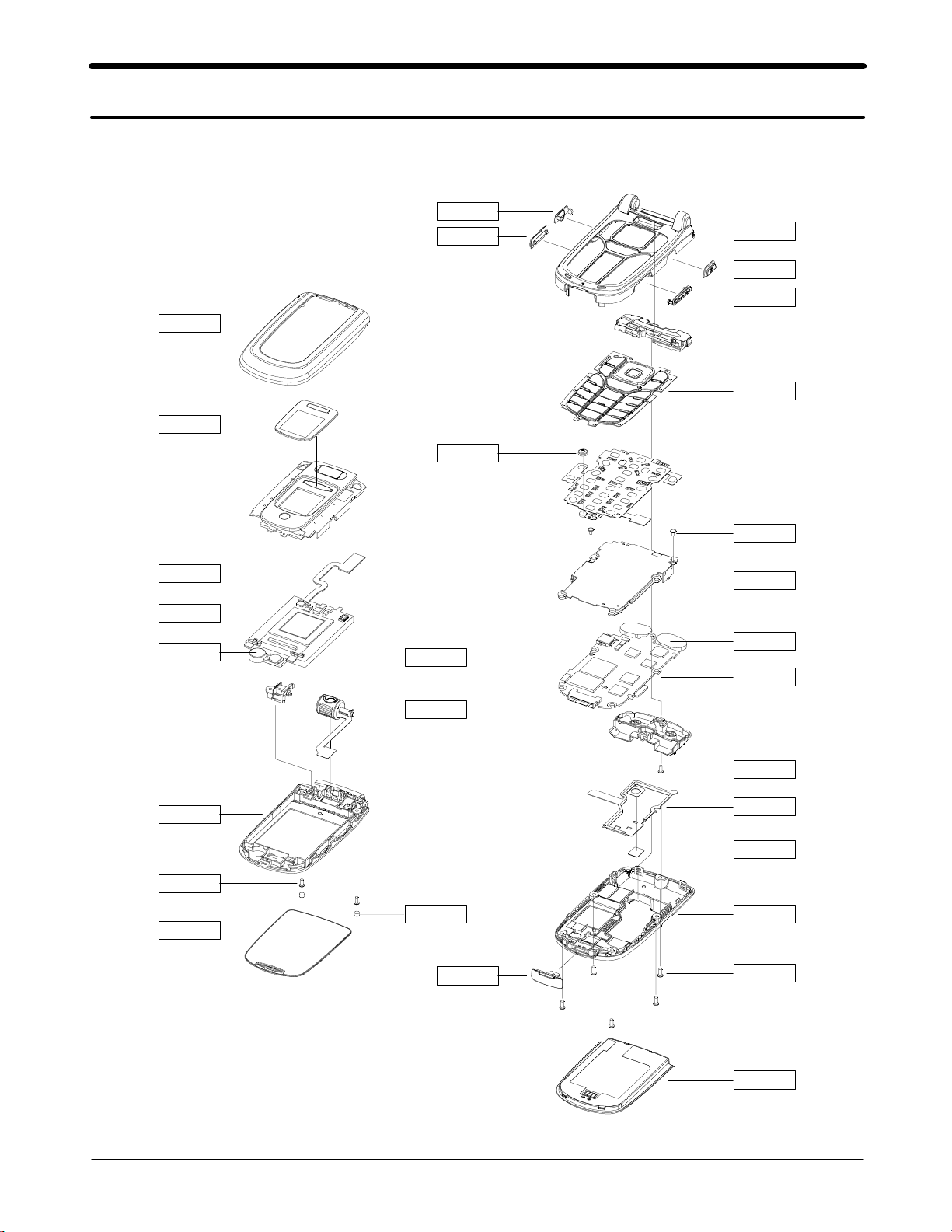
3. Exploded View and Parts List
3-1. Exploded View
QRF03
QVO01
QFU01
QWD01
QMI03
QFR01
QCK01
QCW04
QKP01
QCR12
QME03
QLC01
QMO01
QFL01
QCR16
QMW01
QAR01
QCA01
QSC12
QIF01
QFR02
QME06
QMP01
QCR04
QRE02
QRF01
QRE01
QCR11
3-1
SAMSUNG Proprietary-Contents may change without notice
This Document can not be used without Samsung's authorization
QBA01

Exploded view and Part List
3-2. Parts List
Location No Description Sec Code
QAR01
QBA01
QCA01
QCK01
QCR04
QCR11
QCR12
QCR16
QFL01
QFR02
QFU01
QIF01
QKP01
QLC01
QME03
QME06
QMO01
QMP01
QMW01
QRE01
QRE02
QRF01
QSC12
QVO01
QWD01
QFR01
ㅤ
ㅤ
ㅤ
ㅤ
ㅤ
ㅤ
ㅤ
ㅤ
ㅤ
ㅤ
ㅤ
ㅤ
ㅤ
ㅤ
ㅤ
ㅤ
ㅤ
ㅤ
ㅤ
ㅤ
ㅤ
ㅤ
ㅤ
ㅤ
ㅤ
ㅤ
ㅤ
ㅤ
ㅤ
QCW04 PMO-TRANS FLASH COVER;SGH-ZV30,PC,D/ GH72-21805A
QMI03 RMO-RUBBER MIC;SGH-ZV30,205C,5XT2.35 GH73-04677A
QRF03 PMO-EAR JACK COVER;SGH-ZV30,PC+URETH GH72-21806A
AUDIO-RECEIVER;32ohm,110dB±2dB,11x7 3009-001132
BATTERY-1000MAH,SIL,ENG,M;BST474ASB, GH43-01990A
UNIT-CAMERA;SGH-ZV30,MOMFA331U1A,-,E GH59-02281A
MEC-CAMERA KEY;SGH-ZV30,VODAFON,PC,- GH75-06987A
SCREW-MACHINE;PH,+,-,M1.4,L4,ZPC(BLK 6001-001479
SCREW-MACHINE;PH,+,M1.7,L4,ZPC(BLK), 6001-001654
SCREW-MACHINE;PH,+,M1.4,L2.5,ZPC(BLK 6001-001530
SCREW-MACHINE;PH,+,-,M1.7,L4.5,ZPC(B 6001-001878
MEC-FOLDER LOWER;SGH-ZV30,VODAFON,PC GH75-06980A
MEC-FRONT SHIELD CAN;SGH-ZV30,VODAFO GH75-06983A
MEC-FOLDER UPPER;SGH-ZV30,VODAFON,PC GH75-06979A
PMO-IF COVER V2;SGH-ZV30,PC+URETHANE GH72-25828A
MEC-KEYPAD(VOD/D_GRY);SGH-ZV30,VODAF GH75-06982A
LCD-SGHZV30 MODULE;UF-17E101-A,SGH-Z GH07-00754A
UNIT-FPCB;SGH-ZV30,KBSGHZV30KM,-,OMN GH59-02284A
UNIT-SPK MODULE;SGH-ZV30,SS-SGH-ZV30 GH59-02356A
MOTOR DC-SGHZV30;DMJBRK94B,SGH-ZV30, GH31-00177A
PBA MAIN-SGHZV30;SGH-ZV30,VODAFONE,G GH92-02152A
MEC-MAIN WINDOW;SGH-ZV30,VOD,PC,-,-, GH75-07462A
MEC-REAR COVER;SGH-ZV30,VODAFON,PC,- GH75-06985A
MEC-REAR SHIELD CAN;SGH-ZV30,VODAFON GH75-06984A
MPR-SHEET REAR SHIELD CA;SGH-ZV30,PC GH74-15903A
RMO-FOLDER SCREW;SGH-ZV30,SI RUBBER, GH73-05042A
MEC-VOLUME KEY;SGH-ZV30,VODAFON,PC,- GH75-06986A
PCT-SUB WINDOW;SGH-ZV30,ACRYL,SIL,-, GH72-25186A
MEC-FRONT COVER;SGH-ZV30,VODAFON,PC, GH75-06981A
3-2
SAMSUNG Proprietary-Contents may change without notice
This Document can not be used without Samsung's authorization
Exploded view and Part List
Description Sec Code
BAG PE;LDPE,T0.05,W80,L180,TRP,-,- 6902-000634
CBF INTERFACE-PC DATA CABLE;SGH-Z110 GH39-00326A
CHARGER-TCH;TCH137ESE,SGH-X910,AC/DC GH44-00701A
S/W CD-PC STUDIO VODAFONE;SGH-ZV30,S GH46-00168A
UNIT-EARPHONE;SGH-Z107,EM-SS650E-ST, GH59-01713A
LABEL(P)-WATER SOAK;COMM,NORGE,100G, GH68-02026A
MANUAL-WEEE CARD;COMM,SEC,ENGLISH,UN GH68-07013A
LABEL(R)-MAIN;SGH-ZV30,EU,MAT,0.05,4 GH68-07055A
MANUAL-USER;SGH-ZV30,MAN,GERMAN,GERM GH68-07773A
MANUAL-QSG;SGH-ZV30,VD2,GERMAN,GERM, GH68-08167A
CUSHION-CASE LOWER(VOD);SGH-Z105,PUL GH69-02177A
BOX(P)-MENUAL BOX(UMTS);SGH-Z107V,SI GH69-02540C
CUSHION-CASE(UPPER);SGH-Z300,PULP,T0 GH69-02837A
BOX(P)-SGHZV30(UMTS);SGH-ZV30,SC350+ GH69-03235A
IPR-LOCKER SPRING;SCH-750,STS304,-,T GH70-10633A
PMO-BATTERY LOCKER;SGH-ZV30,PC,GRY,- GH72-24503A
MPR-BOHO VNYL CONN V2;SGH-E316,#950, GH74-11112A
MPR-BOHO VINYL TOP F/U;SGH-ZV30,3M 4 GH74-14662A
MPR-BOHO VINYL F/LOWER;SGH-ZV30,3M 4 GH74-14663A
MPR-NON WOVEN FRONT LCD;SGH-ZV30,NON GH74-15896A
MPR-MIC PC SHEET;SGH-ZV30,PC SHEET+T GH74-15897A
MPR-TAPE ALUMINIUM;SGH-ZV30,AL TAPE, GH74-16493A
MPR-GASKET GOLD L;SGH-ZV30,CFPWX290, GH74-16494A
MPR-GASKET GOLD R;SGH-ZV30,CFPWX290, GH74-16495A
MPR-TAPE LCD INSULATION2;SGH-ZV30,3M GH74-16497A
MPR-BOHO VINYL UPPER;SGH-ZV30,PBC,38 GH74-17233A
MPR-SPONGE EAR COVER;SGH-ZV30,SRS PO GH74-17968A
MEC-HANGER;SGH-E710,KORA,-,-,ME/SIL, GH75-03673B
3-3
SAMSUNG Proprietary-Contents may change without notice
This Document can not be used without Samsung's authorization
Exploded view and Part List
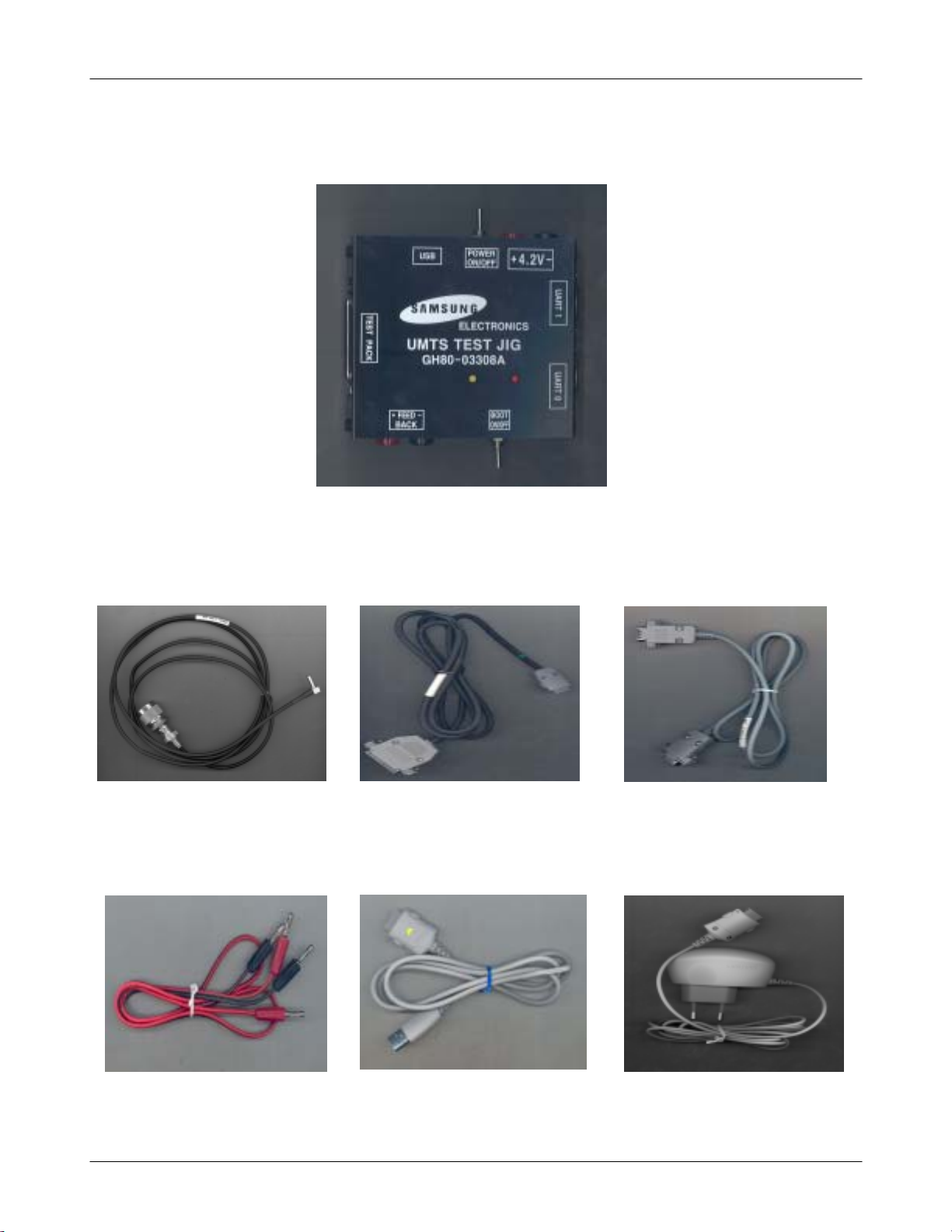
3-3. Test Jig (GH80-03308A)
3-3-1. RF Test Cable
(GH39-00283A)
3-3-2. Test Cable
(GH39-00337E)
3-3-4. Power Supply Cable 3-3-5. DATA CABLE
(
GH39-00326A)
3-3-3. Serial Cable
3-3-6. TC
(GH44-00701A)
3-4
SAMSUNG Proprietary-Contents may change without notice
This Document can not be used without Samsung's authorization
4. Electrical Parts List
Design LOC Description SEC CODE
AN401 ;ACS2450FBAVI 4202-001062
C101,C110,C112,C114 C-CERAMIC,CHIP 2203-000812
C102,C104,C252,C408 C-CERAMIC,CHIP 2203-000679
C103,C107,C129,C137 C-CERAMIC,CHIP 2203-000438
C105,C111,C113,C120 C-CERAMIC,CHIP 2203-005482
C108,C130,C136,C171 C-CERAMIC,CHIP 2203-000254
C115,C116,C117,C119 C-CERAMIC,CHIP 2203-000812
C118,C125,C133,C601 C-CERAMIC,CHIP 2203-000854
C121,C124,C131,C146 C-CERAMIC,CHIP 2203-000812
C122,C126,C132,C134 C-CERAMIC,CHIP 2203-000233
C123,C204 C-CERAMIC,CHIP 2203-000885
C127,C135,C154,C159 C-CERAMIC,CHIP 2203-000995
C128,C141,C142,C150 C-CERAMIC,CHIP 2203-005482
C138 C-FILM,CHIP 2301-001512
C139 C-CERAMIC,CHIP 2203-005446
C140 C-CERAMIC,CHIP 2203-002668
C143,C253 C-CERAMIC,CHIP 2203-000836
C147,C245,C257,C413 C-CERAMIC,CHIP 2203-006208
C148,C153,C162,C168 C-CERAMIC,CHIP 2203-000438
C149,C164,C169,C259 C-CERAMIC,CHIP 2203-000386
C151,C163,C229,C251 C-CERAMIC,CHIP 2203-000812
C152,C156,C157,C207 C-CERAMIC,CHIP 2203-005482
C155,C328,C329,C417 C-CERAMIC,CHIP 2203-006093
C158 C-CERAMIC,CHIP 2203-000311
C160,C457 C-TA,CHIP 2404-001274
C161 C-FILM,CHIP 2301-001515
C165 C-CERAMIC,CHIP 2203-005503
C166 C-CERAMIC,CHIP 2203-002443
C167,C221 C-CERAMIC,CHIP 2203-005234
C170,C201,C202,C209 C-CERAMIC,CHIP 2203-000233
C205 C-CERAMIC,CHIP 2203-006324
C208,C210,C214,C248 C-CERAMIC,CHIP 2203-000330
C211,C685 C-CERAMIC,CHIP 2203-000995
C212 C-CERAMIC,CHIP 2203-001178
C222 C-CERAMIC,CHIP 2203-001383
C224,C228,C234,C244 C-CERAMIC,CHIP 2203-000233
C225,C233,C238,C240 C-CERAMIC,CHIP 2203-005482
C231,C232,C235,C239 C-CERAMIC,CHIP 2203-000254
C236,C242 C-CERAMIC,CHIP 2203-005288
C237,C241,C256,C407 C-CERAMIC,CHIP 2203-000438
C243,C246,C249,C258 C-CERAMIC,CHIP 2203-005482
C247,C250,C262,C404 C-CERAMIC,CHIP 2203-000233
C254 C-CERAMIC,CHIP 2203-000585
C255 C-FILM,CHIP 2301-001214
C260,C261,C684 C-CERAMIC,CHIP 2203-005050
C263 C-CERAMIC,CHIP 2203-000330
C301,C303,C304,C305 C-CERAMIC,CHIP 2203-005482
C302,C310 C-CERAMIC,CHIP 2203-006091
C306,C307,C308,C309 C-CERAMIC,CHIP 2203-005482
C311,C312,C313,C314 C-CERAMIC,CHIP 2203-005482
4-1
SAMSUNG Proprietary-Contents may change without notice
This Document can not be used without Samsung's authorization
Electrical Parts List
Design LOC Description SEC CODE
C315,C316,C317,C318 C-CERAMIC,CHIP 2203-005482
C319,C320,C321,C322 C-CERAMIC,CHIP 2203-005482
C323,C324,C325,C326 C-CERAMIC,CHIP 2203-005482
C333,C334,C335,C336 C-CERAMIC,CHIP 2203-005482
C337,C338,C339,C340 C-CERAMIC,CHIP 2203-005482
C341,C342 C-CERAMIC,CHIP 2203-000550
C343 C-CERAMIC,CHIP 2203-000489
C344 C-CERAMIC,CHIP 2203-005480
C345 C-CERAMIC,CHIP 2203-000254
C346,C402,C406,C409 C-CERAMIC,CHIP 2203-005482
C347,C501,C638,C647 C-TA,CHIP 2404-001225
C348 C-CERAMIC,CHIP 2203-005395
C401,C481 C-CERAMIC,CHIP 2203-006053
C405 C-CERAMIC,CHIP 2203-000628
C410,C414,C416,C419 C-CERAMIC,CHIP 2203-005482
C415,C422,C423,C431 C-CERAMIC,CHIP 2203-006208
C418,C420,C425,C426 C-CERAMIC,CHIP 2203-006201
C421,C427,C430,C432 C-CERAMIC,CHIP 2203-000278
C424,C440,C442,C458 C-CERAMIC,CHIP 2203-005482
C428,C429,C462 C-CERAMIC,CHIP 2203-006201
C433,C467,C472,C475 C-CERAMIC,CHIP 2203-006093
C434,C603,C604,C606 C-CERAMIC,CHIP 2203-000278
C441 C-CERAMIC,CHIP 2203-001153
C443,C444,C605,C683 C-CERAMIC,CHIP 2203-000812
C446,C449,C450,C451 C-CERAMIC,CHIP 2203-000438
C447,C448 C-CERAMIC,CHIP 2203-006208
C452,C453,C454,C466 C-CERAMIC,CHIP 2203-000438
C460,C461 C-TA,CHIP 2404-001281
C463,C502,C503 C-TA,CHIP 2404-001105
C464 C-CERAMIC,CHIP 2203-002494
C470,C471,C504,C512 C-CERAMIC,CHIP 2203-005482
C473,C474 C-CERAMIC,CHIP 2203-005138
C478,C505,C649 C-TA,CHIP 2404-001339
C479,C506,C650,C693 C-CERAMIC,CHIP 2203-005061
C482,C508,C509,C510 C-CERAMIC,CHIP 2203-006093
C483,C507,C517,C518 C-CERAMIC,CHIP 2203-000233
C511,C615,C622,C670 C-CERAMIC,CHIP 2203-006093
C513,C514,C633,C634 C-CERAMIC,CHIP 2203-005482
C602,C607,C608,C629 C-CERAMIC,CHIP 2203-000854
C609,C613 C-TA,CHIP 2404-001366
C614,C621,C681 C-CERAMIC,CHIP 2203-006137
C616,C617 C-TA,CHIP 2404-001352
C618 C-CERAMIC,CHIP 2203-000233
C630 C-CERAMIC,CHIP 2203-000438
C632,C635,C636,C678 C-CERAMIC,CHIP 2203-000854
C637,C640,C671,C690 C-CERAMIC,CHIP 2203-005482
C639,C691 C-TA,CHIP 2404-001394
C641,C642,C643,C644 C-CERAMIC,CHIP 2203-005481
C645,C646 C-CERAMIC,CHIP 2203-000654
C648,C692 C-TA,CHIP 2404-001225
4-2
SAMSUNG Proprietary-Contents may change without notice
This Document can not be used without Samsung's authorization

Electrical Parts List
Design LOC Description SEC CODE
C679,C682,C686,C687 C-CERAMIC,CHIP 2203-000278
C680 C-CERAMIC,CHIP 2203-000854
C688 C-CERAMIC,CHIP 2203-000278
C689 C-CERAMIC,CHIP 2203-006093
C694 C-CERAMIC,CHIP 2203-005061
C695,C696 C-CERAMIC,CHIP 2203-006190
C697,C698 C-CERAMIC,CHIP 2203-000812
CN101 CONNECTOR-COAXIAL 3705-001358
CN401 CONNECTOR-CARDEDGE 3709-001269
CN402 CONNECTOR-SOCKET 3710-002120
CN404 CONNECTOR-HEADER 3711-005781
CN504 CONNECTOR-CARDEDGE 3709-001344
CN505 ;14-5602-060-000-829 3711-005367
CN601 JACK-PHONE 3722-002181
CN603,CN604 CONNECTOR-SOCKET 3710-001105
D400 DIODE-SCHOTTKY 0404-001093
D401 DIODE-ARRAY 0407-001002
F100 FILTER-SAW 2904-001550
F101 FILTER-SAW 2904-001570
F102 FILTER-SAW 2904-001571
F201 FILTER-SAW 2904-001439
F202 FILTER-SAW 2904-001438
F203 RF-MODULE 4709-001370
F204 FILTER 2910-000004
HEA501 CONNECTOR-HEADER 3711-005643
L101 INDUCTOR-SMD 2703-002201
L102,L121,L124 INDUCTOR-SMD 2703-002155
L103,L106,L112,L119 INDUCTOR-SMD 2703-002198
L104,L204,L213 INDUCTOR-SMD 2703-002267
L105 INDUCTOR-SMD 2703-002200
L108,L114,L115,L120 INDUCTOR-SMD 2703-002819
L109,L111,L116,L118 INDUCTOR-SMD 2703-002208
L110,L117,L203 INDUCTOR-SMD 2703-002205
L113,L208,L211,L212 CORE-FERRITE BEAD 3301-001756
L122 INDUCTOR-SMD 2703-002170
L123 INDUCTOR-SMD 2703-002369
L201 INDUCTOR-SMD 2703-002314
L202 INDUCTOR-SMD 2703-002198
L205 INDUCTOR-SMD 2703-002268
L206 INDUCTOR-SMD 2703-001750
L207 INDUCTOR-SMD 2703-002206
L209,L210 INDUCTOR-SMD 2703-002368
L214 CORE-FERRITE BEAD 3301-001120
L215 INDUCTOR-SMD 2703-001749
L301,L302,L303,L305 R-CHIP 2007-000171
L402,L403 INDUCTOR-SMD 2703-002782
L404 INDUCTOR-SMD 2703-000300
L405,L501,L502,L503 CORE-FERRITE BEAD 3301-001534
L602,L603,L605,L604 INDUCTOR-SMD 2703-001595
LED401 PHOTO-IRDA 0604-001261
4-3
SAMSUNG Proprietary-Contents may change without notice
This Document can not be used without Samsung's authorization

Electrical Parts List
Design LOC Description SEC CODE
OSC101 OSCILLATOR-VCO 2806-001360
OSC201 OSCILLATOR-VCTCXO 2809-001280
OSC202 ;MQL302A1G71 2806-001367
OSC301 RESONATOR-CERAMIC 2802-001182
Q403,Q404 TR-DIGITAL 0504-000168
R101,R312,R323 R-CHIP 2007-000171
R102,R211 R-CHIP 2007-007491
R105,R106,R129,R130 R-CHIP 2007-000138
R108,R109,R111,R112 R-CHIP 2007-000140
R115,R118,R642,R643 R-CHIP 2007-000172
R119,R133,R134 R-CHIP 2007-001217
R120,R121,R635,R636 R-CHIP 2007-003001
R123,R124,R125,R126 R-CHIP 2007-001307
R127,R128 R-CHIP 2007-001301
R132,R402 R-CHIP 2007-007142
R135,R204,R207,R214 R-CHIP 2007-000138
R201,R210,R212 R-CHIP 2007-007314
R209,R314 R-CHIP 2007-000137
R215,R405 R-CHIP 2007-001298
R216,R221,R313,R325 R-CHIP 2007-000140
R218,R411,R503,R504 R-CHIP 2007-000143
R301,R304,R311,R315 R-CHIP 2007-000148
R302,R303,R602 R-CHIP 2007-001339
R316,R317,R318,R319 R-CHIP 2007-000148
R321,R326,R327,R508 R-CHIP 2007-000148
R324,R416,R435,R436 R-CHIP 2007-000171
R403,R414,R417,R443 R-CHIP 2007-000140
R408,R623,R624,R625 R-CHIP 2007-007132
R415,R419,R420,R421 R-CHIP 2007-008542
R423,R424 R-CHIP 2007-008542
Q405 TR-DIGITAL 0504-001050
R107 INDUCTOR-SMD 2703-001180
R116 R-CHIP 2007-007316
R117 R-CHIP 2007-000145
R122 R-CHIP 2007-000174
R131 R-CHIP 2007-000147
R202 R-CHIP 2007-000173
R205 R-CHIP 2007-007318
R206 R-CHIP 2007-007470
R208 R-CHIP 2007-008263
R213 R-CHIP 2007-000163
R220 R-CHIP 2007-007310
R222 R-CHIP 2007-001284
R308 R-CHIP 2007-000636
R309 R-CHIP 2007-000157
R406 R-CHIP 2007-007468
R409 R-CHIP 2007-009117
R410 R-CHIP 2007-007095
R413 R-CHIP 2007-000153
R432 R-CHIP 2007-000162
4-4
SAMSUNG Proprietary-Contents may change without notice
This Document can not be used without Samsung's authorization
Electrical Parts List
Design LOC Description SEC CODE
R437,R438 R-CHIP 2007-007199
R439 R-CHIP 2007-007107
R445,R454,R631,R632 R-CHIP 2007-000171
R447,R448,R449,R450 R-CHIP 2007-008437
R452,R453 R-CHIP 2007-003112
R459 R-CHIP 2007-000146
R460 R-CHIP 2007-007592
R509,R511,R630,R641 R-CHIP 2007-000148
R510 R-CHIP 2007-000166
R605 R-CHIP 2007-008055
R607,R608,R611,R612 R-CHIP 2007-007317
R616 R-CHIP 2007-001325
R626 R-CHIP 2007-007132
R627,R628 R-CHIP 2007-007139
R633,R634,R639,R640 R-CHIP 2007-000171
R637,R638 R-CHIP 2007-003001
TH201 THERMISTOR 1404-001221
U104 IC 1205-002645
U105 IC 1201-002174
U106 IC 1205-002724
U201 IC 1201-001984
U202 ;AWT6252M7P8 1201-002196
U203 IC 1205-002297
U204 TR-DIGITAL 0504-001060
U301 ;KBE00F005M-F411 1108-000005
U302 IC 1205-002527
U401 IC 1203-003335
U402 DIODE-ARRAY 0407-001038
U403 RF-MODULE 4709-001352
U407 DIODE-TVS 0406-001200
U408 BATTERY 4302-001177
U409 IC 1203-002785
U411 ;AAT4280-3 1205-002767
U413 IC 1001-001248
U414 IC 1203-003728
U415 FET-SILICON 0505-001889
U502 ;MIC2211-GKYML 1203-003785
U506,U507,U511 ;ECLAMP2378P 2901-001348
U512,U513,U514,U516 VARISTOR 1405-001161
U601 IC 1001-001261
U602 IC 1203-002860
U603 IC 1204-002316
U604,U605 IC 1001-001265
V501,V502,V503,V504 VARISTOR 1405-001082
V505,V506,V507,V508 VARISTOR 1405-001082
V509,V510,V511,V512 VARISTOR 1405-001082
V601,V602,V603,V604 VARISTOR 1405-001082
XTAL401 CRYSTAL-UNIT 2801-004373
ZD402,ZD407 DIODE-TVS 0406-001197
ZD405 DIODE-ZENER 0403-001547
4-5
SAMSUNG Proprietary-Contents may change without notice
This Document can not be used without Samsung's authorization
 Loading...