

Samsung SGH-X495 Service Manual
GSM TELEPHONE
SGH-X495
GSM TELEPHONE
CONTENTS
1. Specification
2. Circuit Description
3. Exploded Views and Parts List
4. Electrical Parts List
5. Block Diagrams
6. PCB Diagrams
7. Flow Chart of Troubleshooting
his Service Manual is a property of Samsung Electronics Co.,Ltd.
ny unauthorized use of Manual can be punished under applicable
nternational and/or domestic law.
ⓒ
Samsung Electronics Co.,Ltd. June. 2005
Printed in Korea.
Code No.: GH68-07423A
BASIC.
1. Specification
1-1. GSM General Specification
GSM850
Phase 1
Freq. Band[MHz]
Uplink/Downlink
ARFCN range 128~251 512~885 512~810
Tx/Rx spacing 45MHz 95MHz 80MHz
Mod. Bit rate/
Bit Period
Time Slot
Period/Frame Period
Modulation 0.3GMSK 0.3GMSK 0.3GMSK
MS Power 33dBm~5dBm 30dBm~0dBm 30dBm~0dBm
824~849
869~894
270.833kbps
3.692us
576.9us
4.615ms
DCS1800
Phase 1
1710~1785
1805~1880
270.833kbps
3.692us
576.9us
4.615ms
Phase 1
1850~1910
1930~1990
270.833kbps
4.615ms
PC1900
3.692us
576.9us
Power Class 5pcl ~ 19pcl 0pcl ~ 15pcl 0pcl ~ 15pcl
Sensitivity -102dBm -100dBm -100dBm
TDMA Mux 8 8 8
Cell Radius 35Km 2Km 2Km
1-1
SAMSUNG Proprietary-Contents may change without notice
This Document can not be used without Samsung's authorization
Specification
1-2. GSM TX power class
TX Power
control level
5 33±2 dBm
6 31±2 dBm
7 29±2 dBm
8 27±2 dBm
9 25±2 dBm
10 23±2 dBm
11 21±2 dBm
GSM850
TX Power
control level
0 30±3 dBm
1 28±3 dBm
2 26±3 dBm
3 24±3 dBm
4 22±3 dBm
5 20±3 dBm
6 18±3 dBm
DCS1800
TX Power
PCS1900
control level
0 30±3 dBm
1 28±3 dBm
2 26±3 dBm
3 24±3 dBm
4 22±3 dBm
5 20±3 dBm
6 18±3 dBm
12 19±2 dBm
13 17±2 dBm
14 15±2 dBm
15 13±2 dBm
16 11±3 dBm
17 9±3dBm
18 7±3 dBm
19 5±3 dBm
7 16±3 dBm
8 14±3 dBm
9 12±4 dBm
10 10±4 dBm
11 8±4dBm
12 6±4 dBm
13 4±4 dBm
14 2±5 dBm
7 16±3 dBm
8 14±3 dBm
9 12±4 dBm
10 10±4 dBm
11 8±4dBm
12 6±4 dBm
13 4±4 dBm
14 2±5 dBm
15 0±5 dBm
1-2
15 0±5 dBm
SAMSUNG Proprietary-Contents may change without notice
This Document can not be used without Samsung's authorization
2. Circuit Description
2-1. SGH-X495 RF Circuit Description
2-1-1. RX PART
- ASM(U100)→Switching Tx, Rx path for GSM850, DCS1800, PCS1900 by logic controlling.
- ASM Control Logic (U100)
Tx Mode (GSM850) H L L
Tx Mode (DCS1800/1900) L H L
Rx Mode (GSM850) L L L
Rx Mode (DCS1800) L L L
Rx Mode (PCS1900) L L H
- FILTER
To convert Electromagnetic Field Wave to Acoustic Wave and then pass the specific frequency band.
- GSM FILTER (F101)→For filtering the frequency band between 869 and 894 MHz
- DCS FILTER (F102)→For filtering the frequency band between 1805 and 1880 MHz.
- PCS FILTER (F100)→For filtering the frequency band between 1930 and 1990 MHz.
- VC-TCXO (OSC101)
This module generates the 26MHz reference clock to drive the logic and RF. After division by two a reference clock of
13MHz is supplied to the other parts of the system through the pin CLKOUT. After additional process, the reference
clock applies to the U100 Rx IQ demodulator and Tx IQ modulator. And then, the oscillator is controlled by serial data
to select channel and use fast lock mode for GPRS high class operation.
→
Truth Table
VC1 VC2 VC3
- Transceiver (U101)
The receiver front-end which amplifies the GSM, DCS aerial signal, converts the chosen channel down to a low IF signal
of 100 kHz. The first stages are symmetrical low noise amplifiers (LNAs). The LNAs are followed by an IQ down mixer.
It consists of two mixers in parallel but driven by quadrature out of phase LO signals. The In phase (I) and Quadrature
phase (Q) IF signals are low pass filtered to provide protection from high frequency offset interferes. The low IF I and Q
signals are then fed into the channel filter. The front-end low IF I and Q outputs enter the integrated bandpass channel
filter with provision for five 8 dB gain steps in front of the filter.
2-1-2. TX PART
I and Q baseband signals are applied to the IQ modulator that shifts the modulation spectrum up to the transmit IF. It is
designed for low harmonic distortion, low carrier leakage and high image rejection to keep the phase error as small as
possible.
2-1
SAMSUNG Proprietary-Contents may change without notice
This Document can not be used without Samsung's authorization
Circuit Description
The modulator is loaded at its IF output by an integrated low pass filter that suppress unwanted spurs prior to get into
the phase detector. The clock drive is generated by division of the RFLO signal provided for the transmit offset mixer.
Baseband IQ signal fed into offset PLL, this function is included inside of U101 chip. OSC100 chip generates modulator
signal which power level is about 6.5dBm and fed into Power Amplifier(U102). The PA output power and power ramping
are well controlled by Auto Power Control circuit. We use offset PLL below table.
GSM -35dBc
DCS -35dBc
GSM -66dBc
DCS -65dBc
GSM -75dBc
DCS -68dBc
Modulation Spectrum
200kHz offset
30 kHz bandwidth
400kHz offset
30 kHz bandwidth
600kHz ~ 1.8MHz offset
30 kHz bandwidth
2-2. Baseband Circuit description of SGH-X495
2-2-1. PCF50601
- Power Management
Ten low-dropout regulators designed specifically for GSM applications power the terminal and help ensure optimal system
performance and long battery life. A programmable boost converter provides support for 1.8V, 3.0VSIMs, while a selfresetting, electronically fused switch supplies power to external accessories. Ancillary support functions, such as RTC
module and High Voltage Charge pump, Clock generator, aid in reducing both board area and system complexity.
I2C BUS serial interface provides access to control and configuration registers. This interface gives a microprocessor full
control of the PCF50601 and enables system designers to maximize both standby and talk times.
Supervisory functions. including a reset generator, an input voltage monitor, and a temperature sensor, support reliable
system design. These functions work together to ensure proper system behavior during start-up or in the event of a fault
condition(low microprocessor voltage, insufficient battery energy, or excessive die temperature).
-Backlight Brightness Modulator
The Backlight Brightness Modulator (BBM) contains a programmable Pulse-width
to modulate the intensity of a series of LED? s or to control a DC/DC converter that drives LCD backlight.
This phone (SGH-X495) use PWM control to contrast the backlight brightness.
Clock Generato
-
The Clock Generator (CG) generates all clocks for internal and external usage. The 32768 Hz crystal
oscillator provides an accurate low clock frequency for the PCF50601 and other circuitry.
r
2-2
modulator (PWM) and FET
SAMSUNG Proprietary-Contents may change without notice
This Document can not be used without Samsung's authorization

Circuit Description
2-2-2. LCD Connector
LCD is consisted of main LCD(color 65K UFB LCD) and sub LCD (B/W LCD).
Chip select signals LCD_MAIN_CS and LCD_SUB_CS, can enable Each LCD. BACKLIGHT signal enables white LED
of main LCD. "LCD_RESET" signal initiates the reset process of the LCD.
16-bit data lines(HD(0)~HD(15)) transfers data and commands to LCD. Data and commands use "HA(1)" signal. If this
signal is low, inputs to LCD are commands. If it is high, inputs to LCD are data.
The signal which informs the state of LCD is whether input or output, is required. But in this system, there is no input
state from LCD. So only "HA(1)" signal is used to indicate write data or command to LCD. Power signals for LCD are
"VBAT and "VDD3".
"SPK_P" and "SPK_N" are used for audio speaker containing voice or melody. And "VDD_VIB" from PCF50601
enables the motor.
2-2-3. Key
This is consisted of key interface pins among OM6359, KBIO(0:7). These signals compose the matrix. Result of matrix
informs the key status to key interface in the OM6359. Power on/off key is separated from the matrix. So power on/off
signal is connected with PCF50601 to enable PCF50601. Twelve key LEDs are use the "VDD_KEY" as supply voltage.
"FLIP" informs the status of folder (open or closed) to the OM6359. This uses the hall effect IC, A321ELH-SAMSUNG.
A magnet under main LCD enables A321ELH-SAMSUNG.
2-2-4. EMI ESD Filter
This system uses the EMI ESD filter, EMIF09 to protect noise from IF CONNECTOR part.
2-2-5. IF connetor
It is 18-pin connector. They are designed to use VBAT, V_EXT_CHARGE, TXD0, RXD0, RTS0, CTS0, JIG_REC,
CHARGER_OK, RXD1, TXD1, AUX_MIC, AUX_SPK and GND. They connected to power supply IC, microprocessor
and signal processor IC.
2-2-6. Battery Charge Management
A complete constant-current/constant-voltage linear charger is used for single cell lithium-ion batteries.
If TA connected to phone, "+DCVOLT" enable charger IC and supply current to battery.
When fault condition caused, "CHG_ON" signal level change low to high and charger IC stop charging
process.
2-2-7. Audio
EARP_P and EARP_N from OM6359 are connected to the main speaker. MIC_P and MIC_N are connected to the main
MIC. YMU788 is a synthesizer LSI for mobile phones. It is a LSI as an input/output device for sound sources, which is
the mobile phones, such as MP3, AAC, etc, in addition to ringing-melodies.
As a synthesis, YMU788 is equipped 32 voices with different tones. Since the device is capable of simultaneously
generating up to synchronous with the play of the FM sy nthesizer, various sampled voices can be used as sound effects.
Since the play data of YMU788 are interpreted at anytime through FIFO, the length of the data(playing period) is not
limited, so the device can flexibly support application such as incoming call melody music distribution service.
2-3
SAMSUNG Proprietary-Contents may change without notice
This Document can not be used without Samsung's authorization

Circuit Description
The hardware sequencer built in this device allows playing of the complex music without giving excessive load to the
CPU of the portable telephones.
For the purpose of enabling YMU788 to demonstrate its full capabilities, Yamaha purpose to use "SMAF:Synthetic music
Mobile Application Format" as a data distribution format that is compatible with multimedia. Since the SMAF takes a
structure that sets importance on the synchronization between sound and images, various contents can be written into it
including incoming call melody with words that can be used for training karaoke, and commercial channel that combines
texts, images and sounds, and others. The hardware sequencer of YMU788 directly interprets and plays blocks relevant to
synthesis (playing music and reproducing ADPCM with FM sy nthesizer) that are included in data distributed in SMAF.
2-2-8. Memory
Signals in the OM6359 enable two memories. They use two volt supply voltage, VDD3 in the PCF50601 & VDD_1.9V
with a LDO. This system uses Intel's memory, RD38F3050LOZTQ0. It is consisted of 128M bits flash NOR memory and
64M bits SRAM. It has 16 bit data line, HD[0~15] which is connected to OM6359. It has 26 bit address lines,
HA[1~26]. NCSFLASH & NCSRAM signals are chip select. Writing process, HWR_N is low and it enables writing
process to flash memory and SRAM. During reading process, HRD_N is low and it enables reading process to flash
memory and SRAM. Reading or writing procedure is processed after HWR_N or HRD_N is enabled.
2-2-9. OM6359
OM6359 is consisted of ARM core and DSP core. It has
on-chip program ROM
of KBS, JTAG, EMI and UART. ARM core is consisted of EMI, PIC(Programmable Interrupt Controller),
reset/power/clock unit, DMA controller, TIC(Test Interface Controller), peripheral bridge, PPI, SSI(Synchronous Serial
Interface), ACC(Asynchronous communications controllers), timer, ADC, RTC(Real-Time Clock) and keyboard interface.
KBIO(0:7), address lines of DSP core and HD[0~15]. HA[1~26], address lines of ARM core and HD[0~15], data lines of
ARM core are connected to memory, YMU788.
NCSRAM, NCSFLASH in the ARM core are connected to each memory. HWR_N and HRD_N control the process of
memory. External IRQ(Interrupt ReQuest) signals from each units, such as, PMU need the compatible process.
KBIO[0~7] receive the status from key and RXD0/TXD0 are used for the communication using data link
cable(DEBUG_DTR/RTS/TXD/RXD/CTS/DSR).
It has JTAG control pins(TDI/TDO/TCK) for ARM core and DSP core. It receives 13MHz clock in CKI pin from
external TCXO. ADC(Analog to Digital Convertor) part receives the status of temperature, battery type and battery voltage.
in the DSP. It has 4K*32bits ROM and 2K*32bits RAM in the ARM core. DSP is consisted
8x1Kword on-chip program/data RAM, 55 Kwords
2-2-10. TOH2600DGI4KRA(26MHz)
This system uses the 26MHz TCXO, TOH2600DGI4KRA, SEM. AFC control signal from OM6359 controls frequency
from 26MHz x-tal. The clock output frequency of UAA3536 is 13MHz. This clock is connected to OM6359, YMU788.
2-4
SAMSUNG Proprietary-Contents may change without notice
This Document can not be used without Samsung's authorization
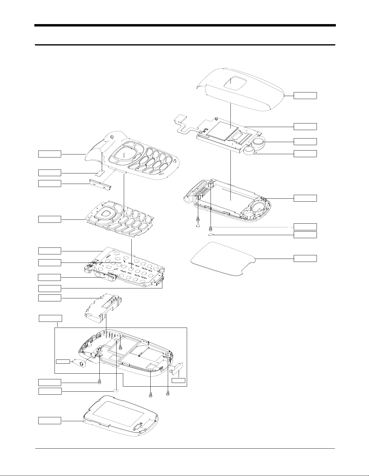
3.Exploded View and PartsList
3-1. Exploded View
QFU01
QLC01
QSP01
QFR01
QSC14
QVO01
QKP01
QMP01
QME01
QVK01
QMI01
QAN02
QRE01
QMO01
QFL01
QCR17
QSC01
QMW02
QCR11
QRF01
QBA01
QRF03
QIF01
3-1
SAMSUNG Proprietary-Contents may change without notice
ThisDocumentcan notbe used without Samsung'sauthorization
Exploded view and PartList
3-2. Parts List
L oc ati on NO. Desc r i pti on SEC COD E
QA N 0 2
QB A 0 1
QC R 1 1
QC R 1 7
QF L0 1
QF R 01
QF U 0 1
QK P 0 1
QL C 01
QM E 0 1
QM I 01
QM O01
QM P 0 1
QMW 0 2
QR F 01
QS C 0 1
QS C 1 4
QS P 01
QV K 0 1
QV O 0 1
QR E 01
ㅤ
ㅤ
ㅤ
ㅤ
ㅤ
ㅤ
ㅤ
ㅤ
ㅤ
ㅤ
ㅤ
ㅤ
ㅤ
ㅤ
ㅤ
ㅤ
ㅤ
ㅤ
ㅤ
ㅤ
ㅤ
ㅤ
ㅤ
ㅤ
QR F 03 PM O -E A R C O V E R ;S G H - X4 9 5,P C W9 15 4 3+ E L A GH 7 2- 23 5 35 B
QIF 01 PM O -I F C O V ER ; SG H-X4 9 5 ,PC G73 7 97 + E LA S GH 7 2-2 3 5 56 B
QMI03 RM O-RU B B E R M IC RE A R ;S G H -X 4 9 7,C R R U B B GH7 3 -0 48 4 7A
INT E N N A -S G H X 49 5 ;IA P T 0G DP4 02 0 H A ,SG H-X GH 4 2- 00 5 74 A
BA TT E R Y- 10 0 0MA H,S IL ,M A IN ;B S T 4 71 A S A,S GH 4 3- 01 7 88 A
SC R EW-MAC H IN E ; PH ,+ ,M1.7 ,L4 ,Z PC (B L K ), 600 1 -0 01 6 54
SC R EW-MAC H IN E ; CH ,+,M 1.7 ,L5 ,Z PC ( BL K ), 6 00 1- 00 1 63 9
ME C -F O LDER L O WE R; SGH -X4 9 5 ,EU ,- ,-,-,- GH 7 5- 06 4 54 A
ME C -F R O N T C O V E R ;S G H -X 4 95 ,E U ,-,-,-,- , GH 7 5- 06 9 66 B
ME C -F O LDER U P P E R ;S G H -X 4 95 ,T -M O B IL E ,- GH7 5- 06 4 71 B
ME C -K E Y PA D ; SGH- X4 9 5 ,T-MO B ILE ,-,-,- ,- GH 7 5- 06 6 17 A
LCD-S G H -X 49 7 MO D U LE ;U G-12 R 16 8 -C ,S G H - GH0 7 -0 07 6 3A
UN IT -MET A L D O M E ;S G H - X4 9 7 ,SS M50 17 P 85 0 GH5 9-0 2 0 46 A
MI C ROPH O N E -A S S Y -S G H X 49 7 ;2 ,13 0 ~ 50 0 u A, GH 3 0- 0 01 98 A
MOTO R DC -S G H Z 1 30 ;DM JB R K 20 C ,S G H -Z 1 30 , GH 3 1 -00 1 5 4D
PB A M A IN - SGHX 4 9 5; SG H-X4 9 5 ,TM B ,U S A ,P B GH 9 2- 02 2 14 A
PC T-WIN D OW M AIN;SGH -X 49 5 ,AC R Y LI C S H E GH 7 2- 19 9 18 B
MP R -R F S H E ET ;S G H -X 4 9 5,P C SH E ET 0 .3 T, GH 7 4- 14 4 35 C
MP R -S C R EW S H E E T;S GH- X4 9 5 ,PC S H E E T 0 . GH 7 4- 13 6 10 B
MP R -T A PE FRONT FPC ;S GH- E3 3 0,3 M 13 52 G H 7 4 -0 88 76 A
SP EA K E R ;0 .5W,8o h m ,8 9 dB ,8 00 H z,1 7 X 13 mm 30 0 1- 00 1 77 9
UN IT -V O L U M E K E Y ;S G H -X 4 97 ,S S V5 0 1 7P 8 60 G H 5 9- 0 20 53 A
ME C -V O L U M E K E Y ;S G H -X 4 95 ,T -M OBIL E ,-,- GH7 5- 07 2 74 B
ME C -R E A R C O V E R ;S G H -X 4 95 ,U S A ,-,-,-,-, G H 75 -0 6 95 9 B
3-2
SAMSUNG Proprietary-Contents may change without notice
ThisDocumentcan notbe used withoutSamsung's authorization

Exploded view and PartList
Des cript ion SEC COD E
BA G P E ;LDPE ,T0 .0 5 ,W 1 20 ,L3 0 0 ,TR P ,-,- 690 2 -0 00 2 96
BA G P E ;LDPE ,T0 .0 5 ,W 8 0,L 14 0 ,T RP ,-,- 1- 690 2 -0 00 2 97
BA G P P ;P P,T 0 .05 ,W 1 4 0 ,L3 00 ,TRP,-,-1 -P 690 2 -0 00 3 77
LCD-S G H X4 9 7 M A I N; U G -1 2 R1 6 8- B ,SG H - X 49 GH 0 7- 00 7 07 A
LCD-S G H X4 9 7 S U B ;U G - 09 B 12 5 -A ,S G H -X 4 97 GH0 7 -0 07 0 8 A
AD A P TO R - SGHR 2 2 5 T AD;TA D 0 3 7J BE ,S G H -R 2 GH 4 4- 00 1 8 4G
UN IT -A WB S IM CA R D ;S G H -X 1 0 5,8 7 44 4 39 4 , GH 5 9- 00 9 43 A
UN IT -E A R P HONE ; SGH- X4 7 5 ,AE P 13 1 S LE ,-,E GH 5 9- 01 7 00 A
LAB E L( R )-WAT E R S O A K T _ M O B IL E; C O M M,-, GH 6 8- 05 9 14 A
LAB E L( R )-T _MO BI LE GU ID E ;S G H -X47 5,-,M GH 6 8- 06 5 81 A
LAB E L( R )-M A IN ( TMB) ;S G H -X 4 95 ,T M B ,POLY G H6 8 -0 69 7 1 A
MA N U A L -U S E R; SGH -X 49 5 ,TM B,EN G LI S H ,U SA GH 6 8- 06 9 76 A
MA N U A L -U S E R; SGH -X 49 5 ,TM B,SP A N IS H ,U SA GH 6 8-0 6 9 77 A
MA N U A L -A G C G UID E; SGH -X4 9 5 ,TMB,E N G L IS GH 6 8- 06 9 78 A
MA N U A L -A C TI VA T IO N CA R D ;S G H - X4 9 5 ,TM B , GH 6 8 -0 73 99 A
LAB E L- D R ;S G H -X 4 95 ,-,P E ,T1 .5,4 5 ,11 ,S I GH 6 8- 07 5 47 A
LAB E L- R F;S G H - X4 9 5,- ,AR T ,T 0.2 ,42 ,3 8,S GH 6 8- 07 5 48 A
LAB E L( R )-U N IT IME I( TMB); SGH -X 49 5 ,TMB GH 6 8- 07 6 87 A
CU S H IO N -SGH X 4 95 ( U N IT C LA M ) ;S G H -X 4 9 5, GH 69 -0 3 05 8 A
CU S H IO N -SGH X 4 95 ( U P C LA M ) ;S G H -X 4 95 ,H I GH 6 9-0 3 0 59 A
CU S H IO N -SGH X 4 95 ( LO W C LA M ); S G H -X 4 95 ,H GH 6 9- 03 0 60 A
BO X (P )-S G H X 4 9 5(I N /B O X _ W A L L); SG H-X4 9 5 GH 6 9- 03 0 76 B
BO X (P )-S G H X 4 9 5(C L A M _ M A S T ER ); SGH- X 49 5 GH 6 9-0 3 13 0 A
BO X (P )-S G H X 4 9 5(P A T T IO N );S G H - X4 9 5 ,SC 3 GH 6 9- 03 1 32 A
PM O -B A T T LOCK E R ;S G H - X4 9 5 ,PC K 2 2 61 ,B L GH 7 2- 19 9 54 B
PC T-WIN D OW SU B ;S G H -X 4 95 ,A C R Y IC S H E ET G H 7 2-1 9 9 64 A
PM O -S T O P P ER ;S GH- X 49 5,P O L Y U R E TH A N E ,W GH 7 2 -2 15 1 7B
RM O-RU B B E R T O P LCD A ;S G H -X 4 9 5,C R RU B GH 7 3- 04 9 23 A
RM O-RU B B E R T O P LCD B ;S G H -X 4 9 5,C R R U B G H 73 -0 49 2 4 A
MP R -B O H O VIN Y L S U B (S -R );S G H - X 49 5 ,ST A G H 7 4 -0 34 2 9B
MP R -B O H O VIN Y L R E A R; SGH- S3 4 2 i,3M 41 8 GH 7 4-1 2 9 05 A
MP R -T A PE W IN D O W S U B; S G H -X 49 5 ,T ES A #4 GH 7 4- 13 2 23 A
MP R -B O H O VIN Y L IF ;S G H -E 7 20 ,# 9 50 ,8 5 X1 GH 7 4- 13 6 06 A
MP R -T A PE W IN D O W M A IN ;S G H - X 49 5 ,3M 94 9 GH 7 4- 13 6 08 A
MP R -B O H O VIN Y L M A IN ; S G H -X 49 5 ,3M 41 8 7 GH74 -1 4 43 1 A
MP R -B O H O VIN Y L M A IN ( S );S G H -X 4 97 ,S P -1 GH 7 4 -1 44 3 1B
MP R -B O H O VIN Y L S U B ;S G H -X 4 95 ,S T -5 55 5, GH 7 4- 14 4 32 A
MP R -T A PE EL;S P H -B 1 2 00 ,3M 85 1 ,5X 3 .5X T G H 7 4-1 4 8 81 A
MP R -T A PE PB A E M I;S G H - X4 9 5 ,G O LD PU T 0 G H 74 -1 54 8 4 A
MP R -B O H O VIN Y L M /T MB(S ) ;S G H -X 4 95 ,S TA G H 7 4- 1 55 17 B
MP R -S P O N G E MO TO R ; S G H -X 49 5 ,S R S,D 8 X T 0. GH 7 4-1 5 6 10 A
MP R -S P O N G E P B A ;S G H -X 4 95 ,S R S ,38 X 64 X T 5 G H 7 4 -1 59 1 1A
MP R -T A PE PB A A ;S G H -X 4 95 ,3 M 8 51 ,3 X 2X T 0 GH7 4 -1 60 6 6A
MP R -B O H O VIN Y L S U B ;S G H -X 4 95 ,S T -5 55 5, GH 7 4- 17 3 02 A
AS -LC D PC B S V C ;S G H -X 4 9 7,L J9 6- 02 1 37 A , GH 8 1- 01 2 19 A
A/S -L C D F P CB SV C ;S G H -X 4 97 ,P O LY M I D E,2 GH 8 1- 01 9 56 A
PA A E TC - M A N U A L;S G H-X4 9 5 ,TM B ,U S A ,M A N U G H 9 9- 10 3 52 A
3-3
SAMSUNG Proprietary-Contents may change without notice
ThisDocumentcan notbe used withoutSamsung's authorization

Exploded view and PartList
3-3. Test Jig (GH80-01909A)
3-3-1. RF Test Cable
(GH39-00283A)
3-3-2. Test Cable
(GH39-00217A)
3-3-4. Power Supply Cable 3-3-5. DATA CABLE
(GH39-00219A)
3-3-3. Serial Cable
3-3-6. TA
(GH44-00184G)
3-4
SAMSUNG Proprietary-Contents may change without notice
ThisDocumentcan notbe used withoutSamsung's authorization

4. Electrical Parts List
Design LOC Description SEC CODE
BAT300 BATTERY 4302-001180
C101 C-CERAMIC,CHIP 2203-000278
C102 C-CERAMIC,CHIP 2203-000812
C103 C-CERAMIC,CHIP 2203-000854
C104 C-CERAMIC,CHIP 2203-000854
C105 C-CERAMIC,CHIP 2203-000278
C106 C-CERAMIC,CHIP 2203-000278
C107 C-CERAMIC,CHIP 2203-000854
C108 C-CERAMIC,CHIP 2203-005057
C109 C-CERAMIC,CHIP 2203-005482
C110 C-CERAMIC,CHIP 2203-005057
C111 C-CERAMIC,CHIP 2203-005482
C112 C-CERAMIC,CHIP 2203-000233
C113 C-CERAMIC,CHIP 2203-000233
C114 C-CERAMIC,CHIP 2203-005482
C115 C-CERAMIC,CHIP 2203-005057
C116 C-CERAMIC,CHIP 2203-005138
C117 C-CERAMIC,CHIP 2203-001383
C118 C-CERAMIC,CHIP 2203-000359
C119 C-CERAMIC,CHIP 2203-000696
C120 C-CERAMIC,CHIP 2203-000836
C121 C-CERAMIC,CHIP 2203-001101
C122 C-CERAMIC,CHIP 2203-005482
C123 C-CERAMIC,CHIP 2203-005057
C124 C-CERAMIC,CHIP 2203-006053
C125 C-CERAMIC,CHIP 2203-000438
C126 C-CERAMIC,CHIP 2203-000233
C127 C-TA,CHIP 2404-001239
C128 C-CERAMIC,CHIP 2203-006141
C129 C-CERAMIC,CHIP 2203-000438
C130 C-CERAMIC,CHIP 2203-006190
C132 C-CERAMIC,CHIP 2203-005503
C133 C-CERAMIC,CHIP 2203-000311
C134 C-CERAMIC,CHIP 2203-000233
C135 C-CERAMIC,CHIP 2203-000254
C136 C-CERAMIC,CHIP 2203-001153
C137 C-CERAMIC,CHIP 2203-000550
4-1
SAMSUNG Proprietary-Contents may change without notice
This Document can not be used without S amsung's authorization

Electrical Parts List
Design LOC Description SEC CODE
C138 C-CERAMIC,CHIP 2203-006137
C139 C-CERAMIC,CHIP 2203-005482
C140 C-CERAMIC,CHIP 2203-000679
C141 C-CERAMIC,CHIP 2203-005482
C142 C-CERAMIC,CHIP 2203-005057
C143 C-CERAMIC,CHIP 2203-000233
C144 C-CERAMIC,CHIP 2203-000254
C145 C-CERAMIC,CHIP 2203-000438
C146 C-CERAMIC,CHIP 2203-000438
C147 C-CERAMIC,CHIP 2203-000438
C152 C-CERAMIC,CHIP 2203-000278
C153 C-CERAMIC,CHIP 2203-000278
C154 C-CERAMIC,CHIP 2203-000995
C155 C-CERAMIC,CHIP 2203-000995
C156 C-CERAMIC,CHIP 2203-000438
C157 C-CERAMIC,CHIP 2203-001239
C158 C-CERAMIC,CHIP 2203-001239
C200 C-CERAMIC,CHIP 2203-005061
C203 C-CERAMIC,CHIP 2203-005061
C204 C-CERAMIC,CHIP 2203-000254
C206 C-CERAMIC,CHIP 2203-005061
C207 C-CERAMIC,CHIP 2203-000254
C208 C-CERAMIC,CHIP 2203-000254
C210 C-CERAMIC,CHIP 2203-006423
C212 C-CERAMIC,CHIP 2203-005061
C213 C-CERAMIC,CHIP 2203-005482
C214 C-CERAMIC,CHIP 2203-000854
C215 C-CERAMIC,CHIP 2203-006423
C216 C-CERAMIC,CHIP 2203-000854
C218 C-CERAMIC,CHIP 2203-005061
C219 C-CERAMIC,CHIP 2203-005482
C220 C-CERAMIC,CHIP 2203-000254
C221 C-CERAMIC,CHIP 2203-006423
C222 C-CERAMIC,CHIP 2203-006423
C223 C-CERAMIC,CHIP 2203-005482
C224 C-CERAMIC,CHIP 2203-000438
C225 C-CERAMIC,CHIP 2203-005482
4-2
SAMSUNG Proprietary-Contents may change without notice
This Document can not be used without S amsung's authorization

Electrical Parts List
Design LOC Description SEC CODE
C300 C-CERAMIC,CHIP 2203-005482
C301 C-CERAMIC,CHIP 2203-006105
C302 C-CERAMIC,CHIP 2203-005482
C304 C-TA,CHIP 2404-001394
C305 C-CERAMIC,CHIP 2203-005482
C306 C-CERAMIC,CHIP 2203-005482
C307 C-TA,CHIP 2404-001374
C308 C-CERAMIC,CHIP 2203-006257
C309 C-CERAMIC,CHIP 2203-005482
C310 C-CERAMIC,CHIP 2203-006208
C311 C-TA,CHIP 2404-001225
C312 C-CERAMIC,CHIP 2203-005395
C313 C-CERAMIC,CHIP 2203-000386
C314 C-CERAMIC,CHIP 2203-005482
C315 C-CERAMIC,CHIP 2203-006257
C316 C-CERAMIC,CHIP 2203-000628
C317 C-CERAMIC,CHIP 2203-006562
C318 C-CERAMIC,CHIP 2203-000628
C319 C-CERAMIC,CHIP 2203-006562
C320 C-CERAMIC,CHIP 2203-006053
C321 C-CERAMIC,CHIP 2203-000885
C322 C-CERAMIC,CHIP 2203-006208
C323 C-CERAMIC,CHIP 2203-006324
C324 C-CERAMIC,CHIP 2203-000812
C325 C-CERAMIC,CHIP 2203-005065
C326 C-TA,CHIP 2404-001225
C327 C-TA,CHIP 2404-001225
C328 C-CERAMIC,CHIP 2203-005482
C329 C-CERAMIC,CHIP 2203-005482
C330 C-CERAMIC,CHIP 2203-005482
C332 C-CERAMIC,CHIP 2203-006257
C333 C-CERAMIC,CHIP 2203-006562
C334 C-CERAMIC,CHIP 2203-006208
C335 C-CERAMIC,CHIP 2203-006208
C336 C-CERAMIC,CHIP 2203-000679
C337 C-CERAMIC,CHIP 2203-006053
C338 C-CERAMIC,CHIP 2203-006208
4-3
SAMSUNG Proprietary-Contents may change without notice
This Document can not be used without S amsung's authorization

Electrical Parts List
Design LOC Description SEC CODE
C339 C-CERAMIC,CHIP 2203-006208
C340 C-CERAMIC,CHIP 2203-006053
C400 C-TA,CHIP 2404-001348
C401 C-CERAMIC,CHIP 2203-000995
C402 C-CERAMIC,CHIP 2203-005482
C403 C-CERAMIC,CHIP 2203-005061
C404 C-CERAMIC,CHIP 2203-006562
C406 C-CERAMIC,CHIP 2203-000278
C407 C-CERAMIC,CHIP 2203-000679
C408 C-CERAMIC,CHIP 2203-005482
C409 C-CERAMIC,CHIP 2203-005061
C410 C-CERAMIC,CHIP 2203-005736
C411 C-CERAMIC,CHIP 2203-000679
C412 C-CERAMIC,CHIP 2203-005482
C413 C-CERAMIC,CHIP 2203-000679
C415 C-CERAMIC,CHIP 2203-000489
C416 C-CERAMIC,CHIP 2203-000679
C418 C-CERAMIC,CHIP 2203-000278
C419 C-CERAMIC,CHIP 2203-006423
C420 C-CERAMIC,CHIP 2203-005736
C421 C-CERAMIC,CHIP 2203-000885
C422 C-CERAMIC,CHIP 2203-000254
C423 C-CERAMIC,CHIP 2203-001153
C424 C-CERAMIC,CHIP 2203-005483
C425 C-CERAMIC,CHIP 2203-005483
C426 C-CERAMIC,CHIP 2203-006562
C429 C-CERAMIC,CHIP 2203-000995
C430 C-CERAMIC,CHIP 2203-000995
C433 C-CERAMIC,CHIP 2203-006562
C435 C-CERAMIC,CHIP 2203-000995
C437 C-CERAMIC,CHIP 2203-006053
C438 C-CERAMIC,CHIP 2203-005482
C439 C-TA,CHIP 2404-001352
C501 C-CERAMIC,CHIP 2203-002443
C502 C-CERAMIC,CHIP 2203-005482
C503 C-CERAMIC,CHIP 2203-005482
C504 C-CERAMIC,CHIP 2203-000278
4-4
SAMSUNG Proprietary-Contents may change without notice
This Document can not be used without S amsung's authorization

Electrical Parts List
Design LOC Description SEC CODE
C505 C-CERAMIC,CHIP 2203-000679
C507 C-CERAMIC,CHIP 2203-000995
C508 C-CERAMIC,CHIP 2203-000278
C509 C-CERAMIC,CHIP 2203-000995
C510 C-CERAMIC,CHIP 2203-000995
C511 C-CERAMIC,CHIP 2203-000278
C513 C-CERAMIC,CHIP 2203-006562
C514 C-CERAMIC,CHIP 2203-006562
C515 C-CERAMIC,CHIP 2203-006562
CN300 CONNECTOR-CARD EDGE 3709-001355
CN502 CONNECTOR-SOCKET 3710-001611
CN503 CONNECTOR-HEADER 3711-005783
CON101 CONNECTOR-COAXIAL 3705-001358
EAR400 JACK-PHONE 3722-002067
F100 FILTER-SAW 2904-001571
F101 FILTER-SAW 2904-001580
F102 FILTER-SAW 2904-001570
HEA1 CONNECTOR-HEADER 3711-005728
L101 INDUCTOR-SMD 2703-002207
L102 INDUCTOR-SMD 2703-002199
L103 INDUCTOR-SMD 2703-002207
L104 INDUCTOR-SMD 2703-002203
L105 INDUCTOR-SMD 2703-002700
L106 INDUCTOR-SMD 2703-001726
L107 INDUCTOR-SMD 2703-002308
L108 INDUCTOR-SMD 2703-002700
L109 INDUCTOR-SMD 2703-002308
L110 INDUCTOR-SMD 2703-002308
L111 INDUCTOR-SMD 2703-002199
L112 INDUCTOR-SMD 2703-002368
L113 INDUCTOR-SMD 2703-002201
L114 INDUCTOR-SMD 2703-002368
L115 INDUCTOR-SMD 2703-002203
L116 INDUCTOR-SMD 2703-002368
L117 INDUCTOR-SMD 2703-001708
L300 CORE-FERRITE BEAD 3301-001105
L400 CORE-FERRITE BEAD 3301-001362
4-5
SAMSUNG Proprietary-Contents may change without notice
This Document can not be used without S amsung's authorization
Electrical Parts List
Design LOC Description SEC CODE
L401 CORE-FERRITE BEAD 3301-001362
L402 CORE-FERRITE BEAD 3301-001105
L403 CORE-FERRITE BEAD 3301-001105
L501 CORE-FERRITE BEAD 3301-001438
LED501 LED 0601-001790
LED502 LED 0601-001790
LED503 LED 0601-001790
LED504 LED 0601-001790
LED505 LED 0601-001790
LED506 LED 0601-001790
LED507 LED 0601-001790
LED508 LED 0601-001790
LED509 LED 0601-001790
LED510 LED 0601-001790
LED511 LED 0601-001790
LED512 LED 0601-001790
OSC100 OSCILLATOR-VCO 2806-001326
OSC101 OSCILLATOR-VCTCXO 2809-001281
Q100 TR-DIGITAL 0504-001151
R101 R-CHIP 2007-000162
R102 R-CHIP 2007-000162
R103 R-CHIP 2007-000162
R104 R-CHIP 2007-007148
R105 R-CHIP 2007-000141
R106 R-CHIP 2007-007528
R107 R-CHIP 2007-001288
R108 R-CHIP 2007-000171
R109 R-CHIP 2007-001329
R110 R-CHIP 2007-000144
R111 R-CHIP 2007-001308
R112 R-CHIP 2007-001308
R113 R-CHIP 2007-000566
R114 R-CHIP 2007-000148
R115 R-CHIP 2007-001288
R116 R-CHIP 2007-007311
R117 R-CHIP 2007-000566
R118 R-CHIP 2007-007699
4-6
SAMSUNG Proprietary-Contents may change without notice
This Document can not be used without S amsung's authorization

Electrical Parts List
Design LOC Description SEC CODE
R119 R-CHIP 2007-007699
R120 R-CHIP 2007-001308
R121 R-CHIP 2007-001308
R122 R-CHIP 2007-000171
R123 R-CHIP 2007-000171
R125 R-CHIP 2007-008672
R126 R-CHIP 2007-001308
R127 R-CHIP 2007-000142
R128 R-CHIP 2007-000148
R129 R-CHIP 2007-000138
R130 R-CHIP 2007-008213
R131 R-CHIP 2007-008213
R132 R-CHIP 2007-008213
R133 R-CHIP 2007-008213
R134 R-CHIP 2007-000140
R135 R-CHIP 2007-000140
R136 R-CHIP 2007-000171
R200 R-CHIP 2007-000174
R201 R-CHIP 2007-008055
R204 R-CHIP 2007-000162
R205 R-CHIP 2007-008055
R206 R-CHIP 2007-008055
R207 R-CHIP 2007-008055
R208 R-CHIP 2007-008052
R209 R-CHIP 2007-008516
R210 R-CHIP 2007-008055
R211 R-CHIP 2007-007107
R212 R-CHIP 2007-007142
R213 R-CHIP 2007-007001
R214 R-CHIP 2007-007142
R215 R-CHIP 2007-001284
R216 R-CHIP 2007-000148
R217 R-CHIP 2007-001284
R218 R-CHIP 2007-000162
R219 R-CHIP 2007-000162
R220 R-CHIP 2007-007107
R221 R-CHIP 2007-007001
4-7
SAMSUNG Proprietary-Contents may change without notice
This Document can not be used without S amsung's authorization
 Loading...