

Samsung SGH-R210 Troubleshooting
5. Flow Chart of Troubleshooting and Circuit Diagrams
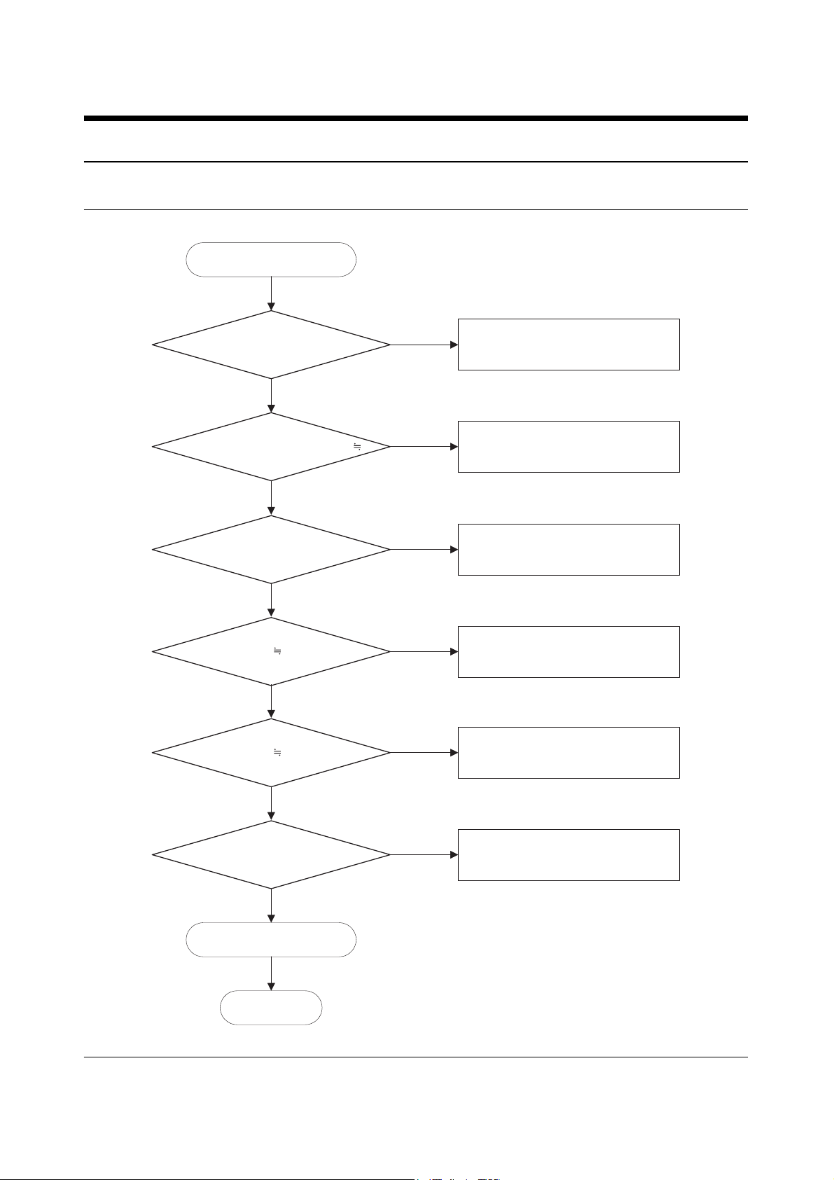
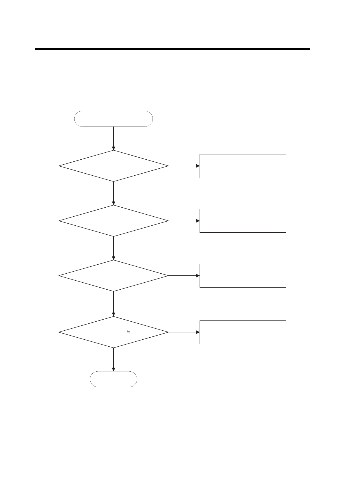
5-1 Power ON
Flow Chart of Troubleshooting and Circuit Diagrams 5-1
'POWER ON'does not work
Charge the Battery
Check the Battery Voltage
is more than 3.2V
No
Yes
Yes
Check the Dome sheet
When the "END" key is
pressed, the voltage of "D304 pin1"
3.6V?
No
Yes
U474 pin 2,3 > 3.2V Check the circuit related to U474
No
END
U619 pin 5 3.0 V ? Check the circuit related to U619
No
Yes
Check the initial operation
U620 pin 5 3.0 V ? Check U620 and related circuit
No
Yes
Check for the clock signal at R107
Check the clock generation circuit
(related to U100 and Q100)
No
Yes
Yes
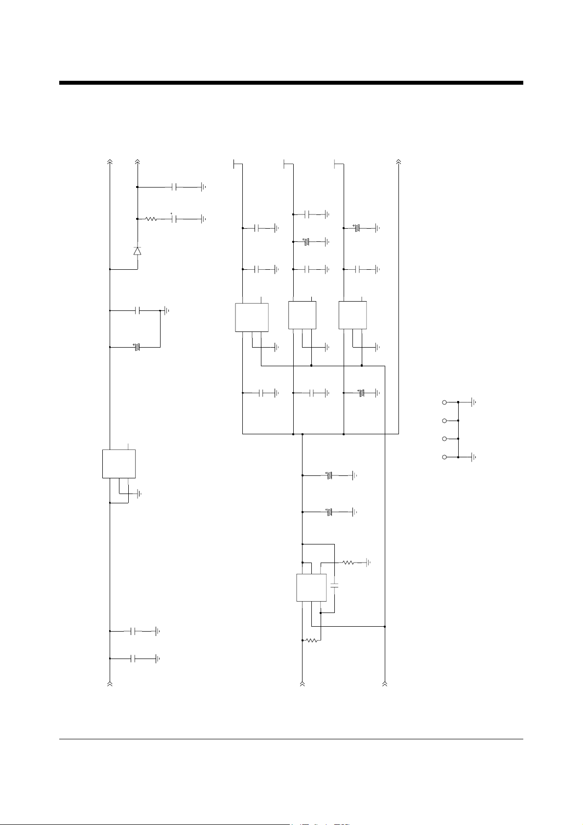
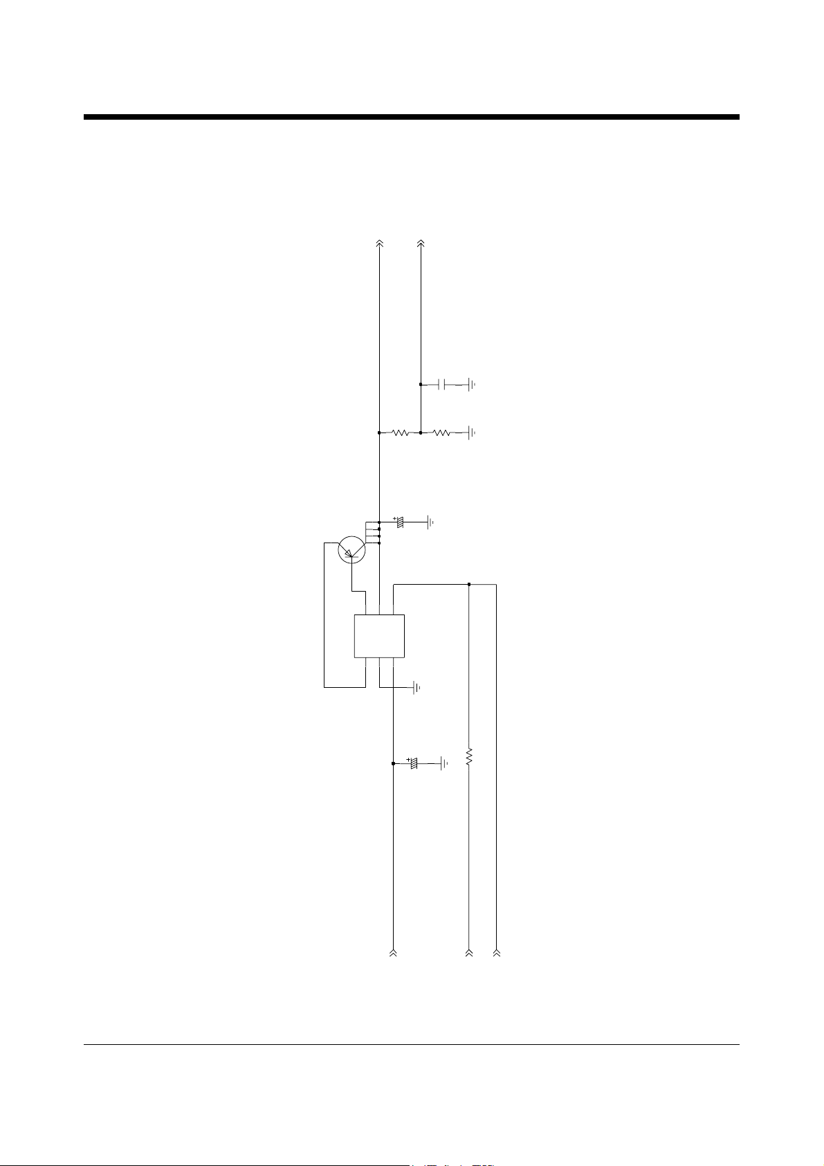
Flow Chart of Troubleshooting and Circuit Diagrams5-2
R2
4
S2
PCB FIXING HOLES(1.9)
One Point Contact
SI3865DV
U474
2
D23D2
5
ON/OFF
R1,C1
61
C328
10UF/6.3V
10NF
C326
C536
10NF
1UF
ALERT_VCC
R738
C748
1K
2
GND
NC
43
ON/OFF
VIN
15
VOUT
10UF/6.3V
C535
D441
MCL4154
U621
LP2981AIM5X-3.3
H403
100UF
C579
100NF
C427
1
VIN VOUT
5
C751
100NF
LP2981AIM5X-3.0
U620
2
GND
4
NC
ON/OFF
3
100K
R583
H400
100PF
C305
10UF/6.3V
C306
C555
27PF
10NF
C307
BAT1
RB414
1K
R584
10NF
C587
1UF
1UF
C749
H401
C318
10NF
C319
VCC
AVCC
GND
2
4
NC
ON/OFF
3
VIN
1
5
VOUT
U619
LP2981AIM5X-3.0
H402
10UF/6.3V
C750
LP2981AIM5X-3.3
U470
2
GND
4
NCON/OFF
3
VIN
15
VOUT
RTC_VCC
VOUT
C436
100UF
+VBATT
+VBATT
RTC_3V3
POWER
Flow Chart of Troubleshooting and Circuit Diagrams 5-3
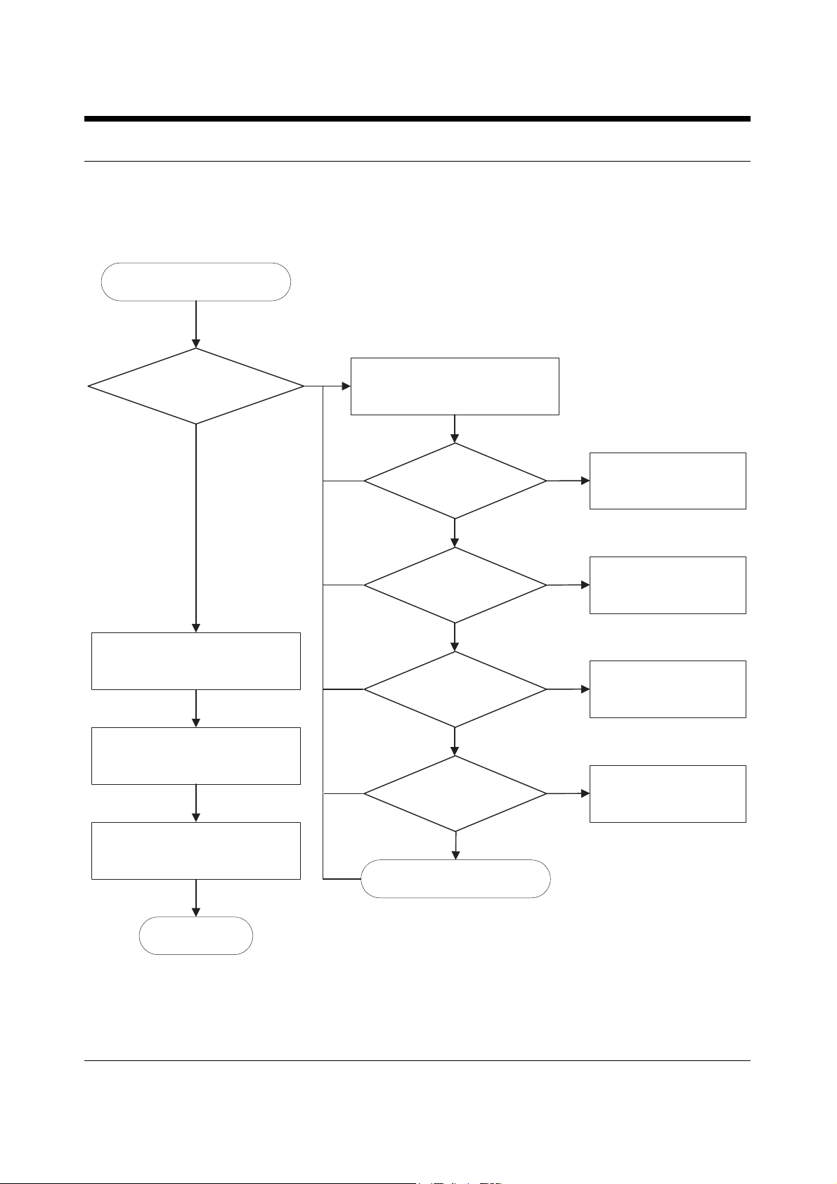
5-2 Initial
Initial Failure
After power on,
check and repair the important
signals of U618 as follows
END
No
Downloading SW is OK ?
(Is CSROM signal OK ?)
The node
between R661 and C712
= "H" (RST)
No
Check the circuit
related to reset
R348 = "H" (BOOT)
No
Resolder R348
Yes
R440 = "H" (MSIZE)
No
Resolder R440
Yes
R438 = "L" (EXTPROC)
No
Resolder R438
Yes
Replace PBA
Check all the other connection
by Test S/W
Check the circuit around LCD
Check the circuit
around U617(EEPROM)
and data stored in it
Yes
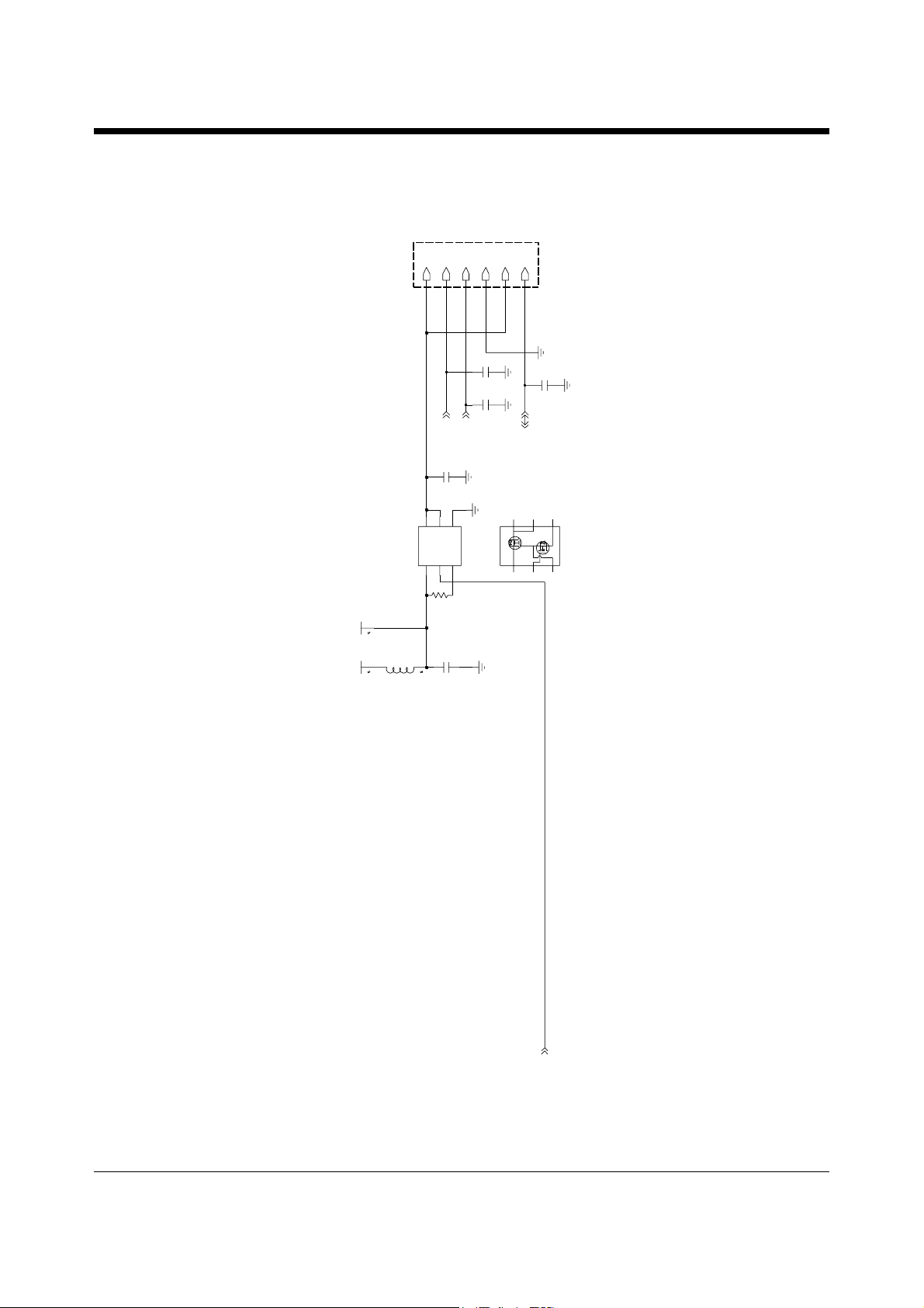
Flow Chart of Troubleshooting and Circuit Diagrams5-4
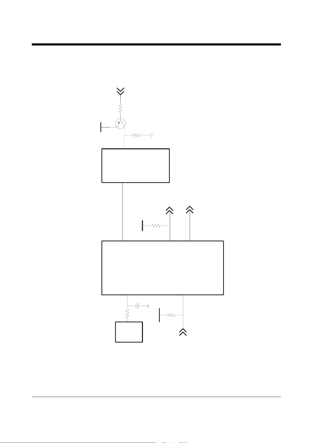
U618
U475
U466
VCC
VCC
R661
C712
R348
R440
R654
VCC
SIM_5V3V
SIMPWDN_BOOT
F_WP
F_WP
F_VCCW
SYSRST
GPIO3
MSIZE
GPO2
Q404
R655
CSROM _CE
Flow Chart of Troubleshooting and Circuit Diagrams 5-5
5-3 Charging Part
Abnormal charging part
Replace T ACheck the J403 pin 17,18 > 4.9 V ?
No
Yes
Yes
Check the U614 pin 3 > 4.9 V ? Resolder C710
Yes
No
R594(CHG_ON side) = "L" ? Resolder R594
Yes
No
Resolder components around
U614
Check the U614 pin 5 4.2V ?
END
Yes
No
Flow Chart of Troubleshooting and Circuit Diagrams5-6
4
L:ON, H: OFF
ZXT13P20DE6
Q405
3
1256
100NF
100K,1%
R658 C711
R659
82K,1%
6.3V
10UF
C708
10V
10UF
C710
VSENSE
5
R594
2.7K,1%
6
DRIVE
2
GND
ISENSE
1
4
PROGVCC
3
DCVOLT
CHG_ON
+VBATT
I_CHARGE
BAT_VOLT
LTC1734ES6-4.2#TR
U614
Flow Chart of Troubleshooting and Circuit Diagrams 5-7
5-4 Sim Part
Q402 pin5 = "H" ?
Replace Q402 or
Replace PBA
END
Yes
No
Check the circuit around U617
(Serial EEPROM) and data stored in it
Yes
Phone can't access SIM card
Yes
Q402 pin 2, 3 = 3.0 V ?
Replace Q402 or
Resolder C434
Yes
No
After Power ON,
Check SIMCLK Signal on J402 pin 3
in a few second
After SIM card insert,
J402 pin 2 = "H(SIMRST) ?
Resoldering C718 or
Replace PBA
Resoldering C764 or
Replace PBA
Yes
No
No
Q402 pin4 = 3.0 V ?
Yes
No
Check the circuit around U620
Flow Chart of Troubleshooting and Circuit Diagrams5-8
BLM10A121S
L605
SIMPWREN
SI1865DL
10NF
J402-11J402-2
2
VCC
C434
SIMCLK
SIMDATA
SIMRST
1UF
C431
C719
100PF
C764
J402-6
6
J402-3
3
100PF
SIMVCC
5
3
1
SIM CONNECTOR
(GND)
6
R2
S2
4
J402-44J402-5
5
10K
R430
(CLK)
(RST)
(VCCSIM)
(SIMDATA)
(VPP)
2
4
FDG6323L
Q402
D22D2
3
ON/OFF
5
6
R1,C1
1
100PF
C718
 Loading...