

SAMSUNG SGH-R210 Service Manual Troubleshooting
5. Flow Chart of Troubleshooting and Circuit Diagrams
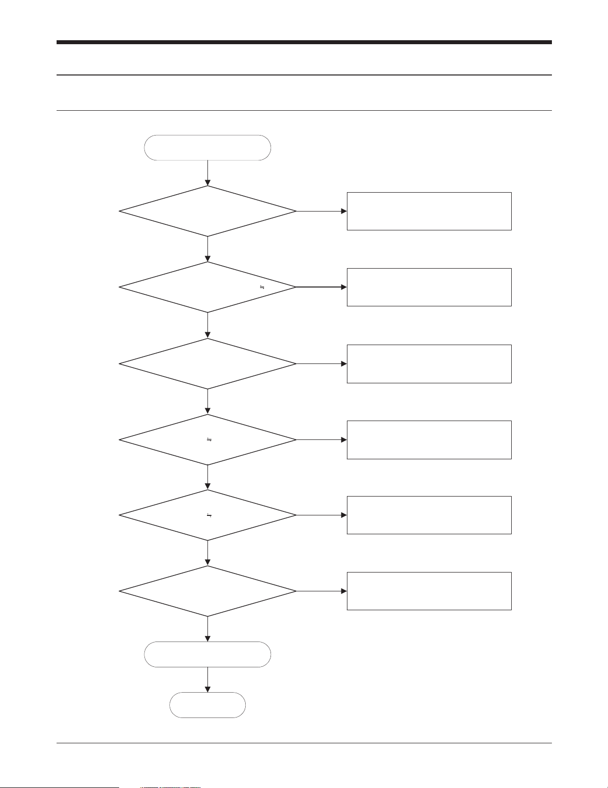
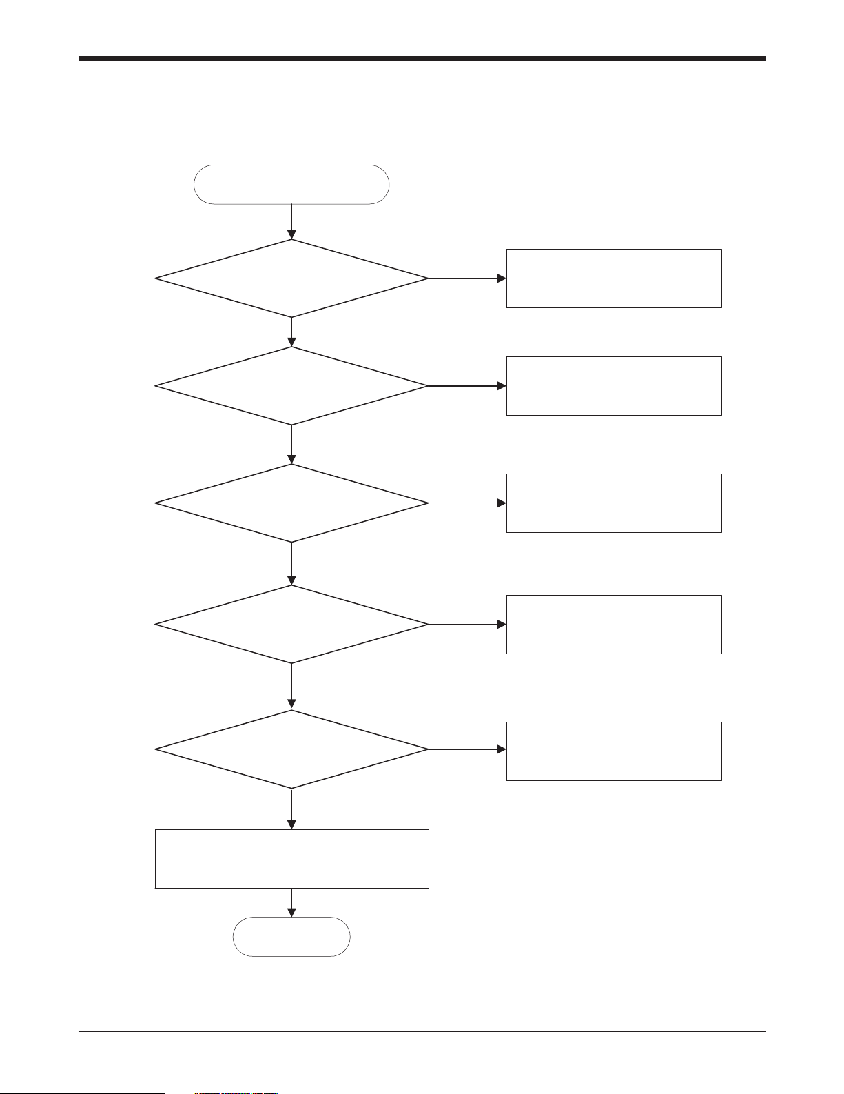
'POWER ON'does not work
Charge the Battery
Check the Battery Voltage
is more than 3.2V
No
Ye s
Ye s
Check the Dome sheet
When the "END" key is
pressed, the voltage of "D304 pin1"
3.6V?
No
Ye s
U474 pin 2,3 > 3.2V Check the circuit related to U474
No
END
U619 pin 5 2.5 V ? Check the circuit related to U619
No
Ye s
Check the initial operation
U620 pin 5 3.0 V ? Check U620 and related circuit
No
Ye s
Check for the clock signal at R107
Check the clock generation circuit
(related to U100 and Q100)
No
Ye s
Ye s
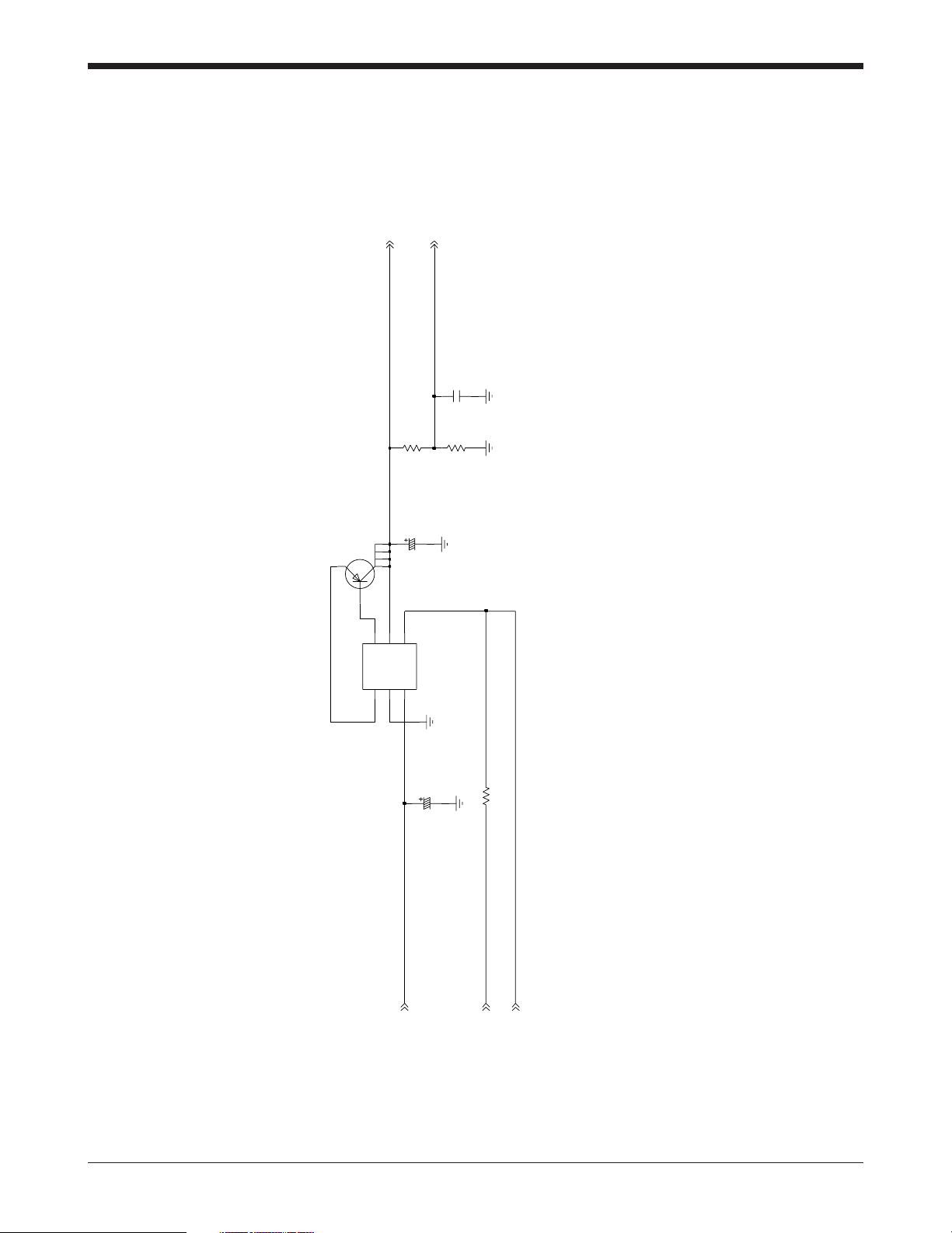
5-1 Power ON
Flow Chart of Troubleshooting and Circuit Diagrams 5-1
ON/OF F
1
VI N V OUT
5
One Point Contact
PCB FIXING HOLES(1.9)
LP2981AIM5X-3.3
U621
GND
2
NC
4
3
1
VIN VOUT
5
C535
10UF/6.3V
U470
LP2981AIM5X-3.0
GND
2
NC
43
ON/OF F
H401 H402 H403H400
R738
1K
C587
10N F
1K
100N F
C751
R1,C 1 R 2
1
S2
4
R584
U474
SI3865D V
D22D2
3
ON/OF F
5
6
C749
1U F
1U F
C318
5
VOUT
1U F
C748
U620
LP2981AIM5X-3. 0
GND
2
NC
43
ON/OF F
VI N
1
MCL4154
D441
AVCC
C436
10N F
C536
100U F
10N F
C427
100N F
10N F
C319
VDD3.0
C326
C305
100P F
C307
10N F
RB414
BAT 1
C750
10UF/6.3V
R583
100K
10UF/6.3V
C328
C306
10UF/6.3V
U619
2
GND
NC
43
ON/OF F
1
VIN VOUT
5
C579
100U F
LP2981AIMX-2.5
C555
+VBAT T
RTC_VCC
LVCC
27P F
RTC_3V 3+VBAT T
POWE R
VOUT
Flow Chart of Troubleshooting and Circuit Diagrams5-2
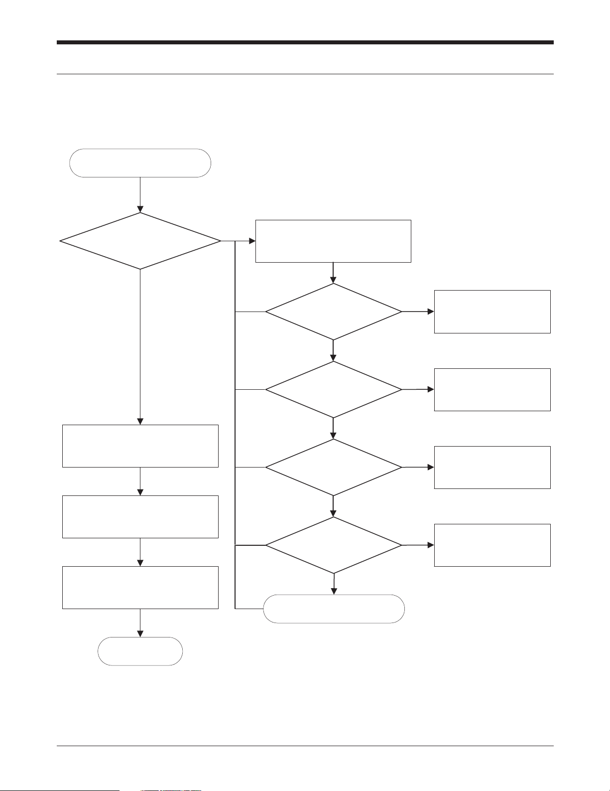
5-2 Initial
Initial Failure
After power on,
check and repair the important
signals of U618 as follows
END
No
Downloading SW is OK ?
(Is CSROM signal OK ?)
The node
between R661 and C712
= "H" (RST)
No
Check the circuit
related to reset
R348 = "H" (BOOT)
No
Resolder R348
Ye s
R440 = "H" (MSIZE)
No
Resolder R440
Ye s
R438 = "L" (EXTPROC)
No
Resolder R438
Ye s
Replace PBA
Check all the other connection
by Test S/W
Check the circuit around LCD
Check the circuit
around U617(EEPROM)
and data stored in it
Ye s
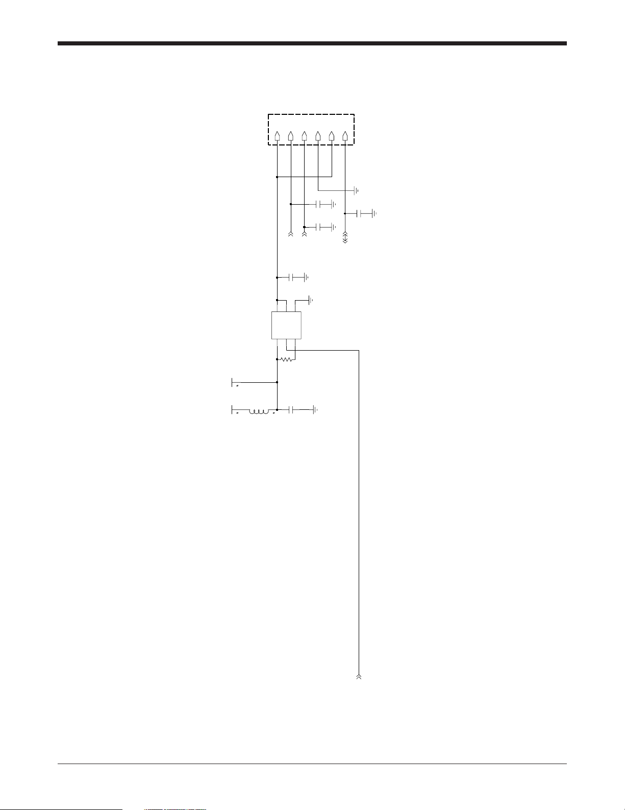
Flow Chart of Troubleshooting and Circuit Diagrams 5-3

U467
U475
U466
VCC
VCC
R661
C712
R348
R440
SIMLEVEL
SIMPWDN_BOOT
_WP/ACC
SYSRST
GPIO3
MSIZE
R655
CSROM _CE
VCC
Flow Chart of Troubleshooting and Circuit Diagrams5-4
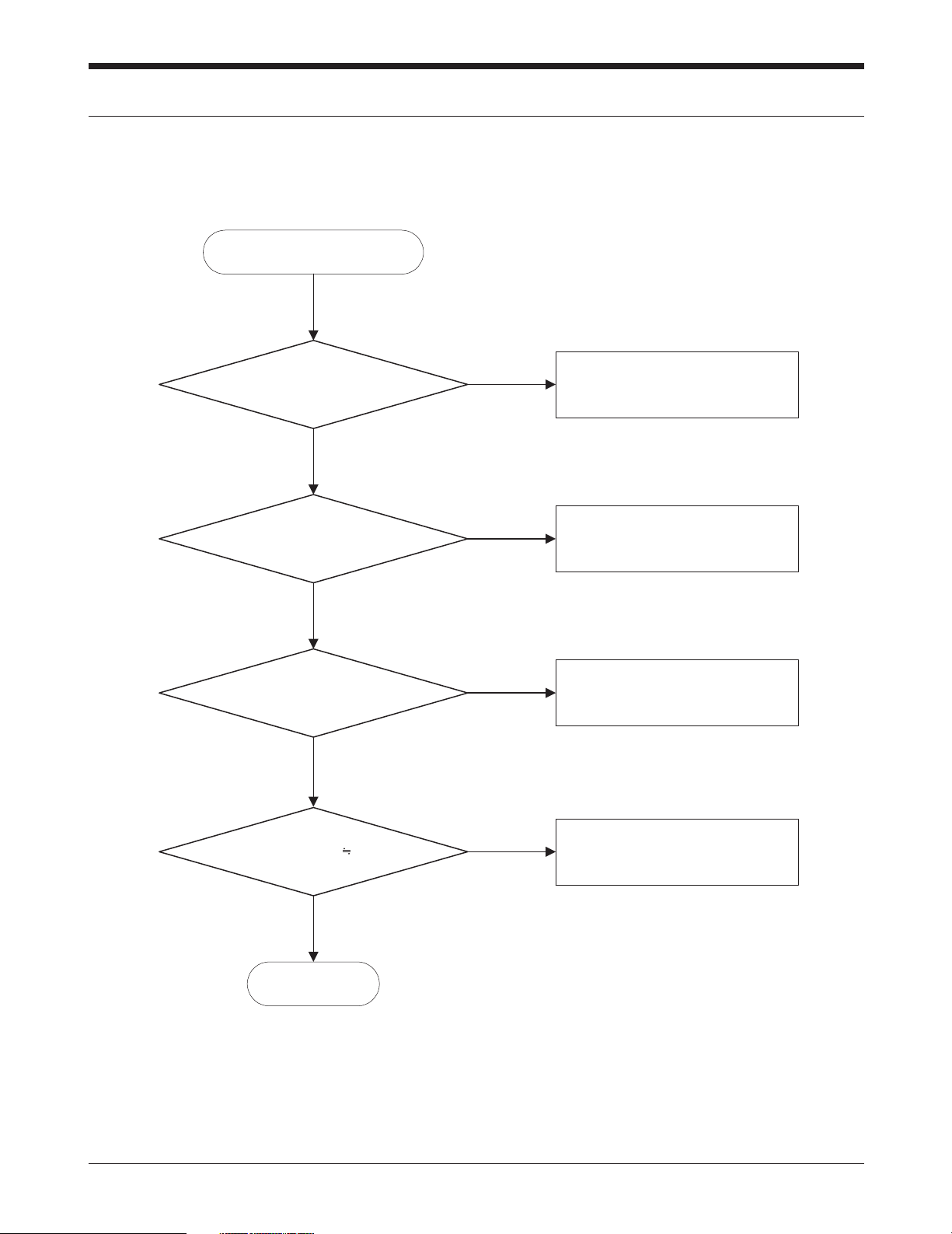
5-3 Charging Part
Abnormal charging part
Replace TACheck the J403 pin 17,18 > 4.9 V ?
No
Ye s
Ye s
Check the U614 pin 3 > 4.9 V ? Resolder C710
Ye s
No
R594(CHG_ON side) = "L" ? Resolder R594
Ye s
No
Resolder components around
U614
Check the U614 pin 5 4.2V ?
END
Ye s
No
Flow Chart of Troubleshooting and Circuit Diagrams 5-5
4
L:ON, H: OFF
ZXT13P20DE6
Q405
3
1256
100NF
100K,1%
R658 C711
R659
82K,1%
6.3V
10UF
C708
10V
10UF
C710
VSENSE
5
R594
2.7K,1%
6
DRIVE
2
GND
ISENSE
1
4
PROGVCC
3
DCVOLT
CHG_ON
+VBATT
I_CHARGE
BAT_VOLT
LTC1734ES6-4.2#TR
U614
Flow Chart of Troubleshooting and Circuit Diagrams5-6
5-4 Sim Part
Q402 pin5 = "H" ?
Replace Q402 or
Replace PBA
END
Ye s
No
Check the circuit around U617
(Serial EEPROM) and data stored in it
Ye s
Phone can't access SIM card
Ye s
Q402 pin 2, 3 = 3.0 V ?
Replace Q402 or
Resolder C434
Ye s
No
After Power ON,
Check SIMCLK Signal on J402 pin 3
in a few second
After SIM card insert,
J402 pin 2 = "H(SIMRST) ?
Resoldering C718 or
Replace PBA
Resoldering C764 or
Replace PBA
Ye s
No
No
Q402 pin4 = 3.0 V ?
Ye s
No
Check the circuit around U620
Flow Chart of Troubleshooting and Circuit Diagrams 5-7
(SIMDATA)
(VCCSIM)
(RST)
(CLK)
(GND)
SIM CONNECTOR
C718
100PF
SIMRST
SIMDATA
SIMCLK
SIMVCCVDD3.0
C431
1UF
10NF
C434
5
J402-66J402-5
J402-1
1
(VPP)
L605
BLM10A121S
SIMPWREN
2
D2
3
ON/OFF
5
6
R1,C1
1
R2
S2
4
100PF
C764
J402-4
4
C719
100PF
J402-22J402-3
3
SI1865DL
Q402
D2
10K
R430
Flow Chart of Troubleshooting and Circuit Diagrams5-8
 Loading...