Samsung SGH-E630 Service Manual
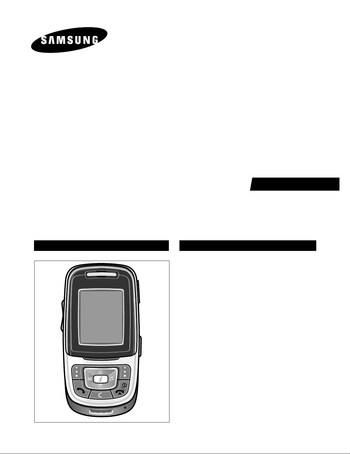
GSM TELEPHONE
SGH-E630
SERVICE
Manual
GSM TELEPHONE CONTENTS
1. Specification
2. Circuit Description
3. Exploded Views and Parts List
4. Electrical Parts List
5. Block Diagrams
6. PCB Diagrams
7. Flow Chart of Troubleshooting

ELECTRONICS
Samsung Electronics Co.,Ltd. Sep. 2004
ⓒ
Printed in Korea.
This Service Manual is a property of Samsung Electronics Co.,Ltd.
Any unauthorized use of Manual can be punished under applicable
International and/or domestic law.
Code No.: GH68-05360A
BASIC.

1. SGH-E630 Specification
1-1
1. GSM General Specification
GSM900
Phase 1
Freq. Band[MHz]
Uplink/Downlink
ARFCN range 1~124
Tx/Rx spacing 45MHz 45MHz 95MHz 80MHz
Mod. Bit rate/
Bit Period
Time Slot
Period/Frame Period
Modulation 0.3GMSK 0.3GMSK 0.3GMSK 0.3GMSK
MS Power 33dBm~13dBm 33dBm~5dBm 30dBm~0dBm 30dBm~0dBm
890~915
935~960
270.833kbps
3.692us
576.9us
4.615ms
EGSM 900
Phase 2
880~915
925~960
0~124 &
975~1023
270.833kbps
3.692us
576.9us
4.615ms
DCS1800
Phase 1
1710~1785
1805~1880
512~885 512~810
270.833kbps
3.692us
576.9us
4.615ms
PCS1900
1850~1910
1930~1990
270.833kbps
3.692us
576.9us
4.615ms
Power Class 5pcl ~ 15pcl 5pcl ~ 19pcl 0pcl ~ 15pcl 0pcl ~ 15pcl
Sensitivity -102dBm -102dBm -100dBm -100dBm
TDMA Mux 8 8 8 8
Cell Radius 35Km 35Km 2Km -
SAMSUNG Proprietary-Contents may change without notice

1-2
SGH-E630 Specification
2. GSM TX power class
TX Power
control level
5 33±2 dBm
6 31±2 dBm
7 29±2 dBm
8 27±2 dBm
9 25±2 dBm
10 23±2 dBm
11 21±2 dBm
GSM900
TX Power
control level
0 30±2 dBm
1 28±3 dBm
2 26±3 dBm
3 24±3 dBm
4 22±3 dBm
5 20±3 dBm
6 18±3 dBm
DCS1800
TX Power
PCS1900
control level
0 30±2 dBm
1 28±3 dBm
2 26±3 dBm
3 24±3 dBm
4 22±3 dBm
5 20±3 dBm
6 18±3 dBm
12 19±2 dBm
13 17±2 dBm
14 15±2 dBm
15 13±2 dBm
16 11±3 dBm
17 9±3dBm
18 7±3 dBm
19 5±3 dBm
7 16±3 dBm
8 14±3 dBm
9 12±4 dBm
10 10±4 dBm
11 8±4dBm
12 6±4 dBm
13 4±4 dBm
14 2±5 dBm
7 16±3 dBm
8 14±3 dBm
9 12±4 dBm
10 10±4 dBm
11 8±4dBm
12 6±4 dBm
13 4±4 dBm
14 2±5 dBm
15 0±5 dBm
15 0±5 dBm
SAMSUNG Proprietary-Contents may change without notice
2. SGH-E630 Circuit Description
1. SGH-E630 RF Circuit Description
1) RX PART
1. FEM(U205)→Switching Tx, Rx path for GSM900, DCS1800 and PCS1900 by logic controlling.
2. ASM Control Logic (U100, U207)→Truth Table
VC_1 VC_2 VC_3
GSM/DCS Rx Mode L L L
PCS Rx Mode L L H
GSM Tx Mode H L L
DCS/PCS Tx Mode L H L
3. FILTER
To convert Electromagnetic Field Wave to Acoustic Wave and then pass the specific frequency band.
- GSM FILTER (L100,L101,L102)→For filtering the frequency band between 925 ~ 960 MHz.
- DCS FILTER (L104,L105,L107)→For filtering the frequency band 1805 and 1880 MHz.
- PCS FILTER (L108, C151, C152)→For filtering the frequency band 1930 and 1990 MHz.
4. TC-VCXO (U101)
To generate the 26MHz reference clock to drive the logic and RF.
After additional process, the reference clock applies to the U100 Rx IQ demodulator and Tx IQ modulator.
The oscillator for RX IQ demodulator and Tx modulator are controlled by serial data to select channel and use fast lock
mode for GPRS high class operation.
5. UAA3536HN (U100)
This chip integrates two differential-input LNAs.
The GSM input supports the E-GSM, DCS input supports the DCS1800. The LNA inputs are matched to the 200 ohm
differential output SAW filters through eternal LC matching network.
Image-reject mixer downconverts the RF signal to a 100 KHz intermediate frequency (IF) with the RFLO from VOL1861
frequency synthesizer. The RFLO frequency is between 1801 ~ 1921 MHz.
The Mixer output is amplified with an analog programmable gain amplifier (PGA), which is controlled by AGAIN.
The quadrature IF signal is digitized with high resolution A/D converts (ADC).
2) TX PART
Baseband IQ signal fed into offset PLL, this function is included inside of U100 chip.
UAA3536HN chip generates modulator signal which power level is about 1.5dBm and fed into Power Amplifier(U201).
The PA output power and power ramping are well controlled by Auto Power Control circuit.
We use offset PLL below table.
2-1
SAMSUNG Proprietary-Contents may change without notice
This Document can not be used without Samsung's authorization
Circuit Description
200kHz offset
30 kHz bandwidth
DCS -35dBc
PCS -35dBc
GSM -66dBc
GSM -35dBc
Modulation Spectrum
400kHz offset
30 kHz bandwidth
DCS -65dBc
PCS -66dBc
GSM -75dBc
600kHz ~ 1.8MHz offset
30 kHz bandwidth
DCS -68dBc
PCS -75dBc
2. Baseband Circuit description of SGH-E630
1. PCF50601
1.1. Power Management
Ten low-dropout regulators designed specifically for GSM applications power the terminal and help ensure optimal system
performance and long battery life. A programmable boost converter provides support for 1.8V, 3.0V, and 5.0V SIMs,
while a self-resetting, electronically fused switch supplies power to external accessories. Ancillary support functions, such
as RTC module and High Voltage Charge pump, Clock generator, aid in reducing both board area and sy stem complexity.
I2C BUS serial interface provides access to control and configuration registers. This interface gives a microprocessor full
control of the PCF50601 and enables system designers to maximize both standby and talk times.
Supervisory functions. including a reset generator, an input voltage monitor, and a temperature sensor, support reliable
system design. These functions work together to ensure proper system behavior during start-up or in the event of a fault
condition (low microprocessor voltage, insufficient battery energy, or excessive die temperature).
1.2. LCD Backlight Brightness Controler (MAX1574)
The Backlight Brightness is controled by Main chip(OM6357_7) through the MAX1574 charge pump.
The MAX1574 charge pump drives three white LED's with regulated constant current for uniform
intensity.
The MAX1574 uses an external resistor to set the full scale 100% LED current. An enable input
(EN-"BACKLIGHT") is used for simple on/off control or can be pulsed repeatedly to set lower LED current in multiple
steps down to 5%. Once the desired brightness is set, the MAX1574 maintains constant LED current as long as EN is
kept high. If EN is kept low for more than 2ms, the MAX1574 enters shutdown.
When the LEDs are enabled by driving EN high, the MAX1574 goes through soft-start, bringing the LED current up to
I
. Dimming is then done by pulsing EN low (500ns to 500µs pulse width). Each pulse reduces the LED current by
LED_
10%, so after one pulse the LED current is 0.9 x I
reduces from 0.1 x I
1.3. Clock Generato
r
LED_
to 0.05x I
. The eleventh pulse sets the LED current back to I
LED
. The tenth pulse reduces the current by 5%, so the I
LED
.
LED_
The Clock Generator (CG) generates all clocks for internal and external usage. The 32768 Hz crystal oscillator provides
an accurate low clock frequency for the PCF50601 and other circuitry.
2-2
SAMSUNG Proprietary-Contents may change without notice
This Document can not be used without Samsung's authorization
LED_
current

Circuit Description
2. Connector
2-1. LCD Connector
LCD is consisted of main LCD(color 65K TFT LCD).
Chip select signals in the
LCD. This signal is from IO part of the DSP in the U300(Main Chip). "LCD_RESET" signal initiates the Reset process
of the LCD.
16-bit data lines(LD(0)~LD(15)) transfers data and commands to LCD through by pass capacitor. Data and commands use
"RS" signal. If this signal is high, Inputs to LCD are commands. If it is low, Inputs to LCD are data. The signal which
informs the input or output state to LCD, is required. But this system is not necessary this signal. So "L_WR" signal is
used to write data or commands to LCD. Power signals for LCD are "VBAT and "VDD2".
"SPK_P" and "SPK_N" from OM6357 are used for audio speaker. And "VDD_VIB" from PCF50601 enables the motor.
2-3. IrDA
This system uses IrDA module, HSDL_3208, Agilent's. This has signals, "IrDA_DOWN" (enable signal), "RXD0" (input
data) and "TXD0" (output data). These signals are connected to OM6357. A power signals, "VDD2" is used for circuit
and LED.
U400
, LCD_MAIN_CS, can enable LCD. BACKLIGHT signal enables white LED of main
2-4. Key
This is consisted of key interface pins among OM6357, KBIO[0~7]. These signals compose the matrix. Result of matrix
informs the key status to key interface in the OM6357. Power on/off key is seperated from the matrix. So power on/off
signal is connected with PCF50601 to enable PCF50601.
Key LED is consisted of four white LED for sub key and six white LED for main key. Key LED use the "BLVDD"
supply voltage. Main key LED is controlled by the "VDD_KEY" supply voltage.
"FLIP" informs the status of folder (open or closed) to the OM6357. This uses the hall effect IC, EM-1681-FT.
A magnet under main LCD enables EM-1681-FT.
2-5. EMI ESD Filter
This system uses the EMI ESD filter, EMIF09 to protect noise from IF CONNECTOR part.
2-6. IF connector
It is 18-pin connector. They are designed to use VBAT, +DCVOLT, TXD0, RXD0, RTS0, CTS0, JIG_REC,
CHARGER_OK, RXD1, TXD1 and GND. They connected to power supply IC, microprocessor and signal processor IC.
3. Battery Charge Management
A complete constant-current/constant-voltage linear charger for single cell lithium-ion batteries.
If TA connected to phone, "+DCVOLT" enable charger IC and supply current to battery.
when fault condition caused, "CHG_ON" signal level change low to high and charger IC stop charging process.
4. Audio
EARP_P and EARP_N from OM6357 are connected to the main speaker. AUXSP is connected to the Hands free kit.
MIC_P and MIC_N are connected to the main MIC. And AUX_MIC_P and AUX_MIC_N are connected to the Hands
free kit.
2-3
SAMSUNG Proprietary-Contents may change without notice
This Document can not be used without Samsung's authorization

Circuit Description
YMU765MA5 is a LSI for portable telephone that is capable of playing high quality music by utilizing FM synthesizer
and ADPCM decorder that are included in this device. As a synthesis, YMU765MA5 is equipped 32 FM voices and 32
Wave Table voices. Since the device is capable of simultaneously generating up to synchronous with the play of the FM
synthesizer, various sampled voices can be used as sound effects.
Since the play data of YMU765MA5 are interpreted at anytime through FIFO, the length of the data(playing period) is
not limited, so the device can flexiblysupport application such as incoming call melody music distribution service.
The hardware sequencer built in this device allows playing of the complex music without giving excessive load to the
CPU of the portable telephones. Moreover, the registers of the FM synthesizer can be operated directly for real time
sound generation, allowing, for example, utilization of various sound effects when using the game software installed in the
portable telephone.
YMU765MA5 includes a speaker amplifier with high ripple removal rate whose maximum output is 580mW
(SPVDD=3.6V). The device is also equipped with conventional function including a vibartor and a circuit for controlling
LEDs synchornous with music.
For the headphone, it is provided with a stereophonic output terminal.
For the purpose of enabling YMU765MA5 to demonstarte its full capablities, Yamaha purpose to use "SMAF:Synthetic
music Mobile Application Format" as a data distribution format that is compatible wiht multimedia. Since the SMAF takes
a structure that sets importance on the synchronization between sound and images, various contents can be written into it
including incoming call melody with words that can be used for traning karaoke, and commercial channel that combines
texts, images and sounds, and others. The hardware sequencer of YMU765MA5 directly interprets and plays blocks
relevant to systhesis (playing music and reproducing ADPCM with FM synthesizer) that are included in data distributed in
SMAF.
5. Memory
signals in the OM6357_7 enable two memories. They use only one volt supply voltage, VDD3 in the PCF50601. This
system uses Samsung's memory, KBB06B400M-F402. It is consisted of 128M bits flash NOR memory and 256M bits
flash NAND memory and 64M bits SCRAM. It has 16 bit data line, HD[0~15] which is connected to OM6357_7 and
MV317S. It has 26 bit address lines, HA[1~26]. CS_NAND and NCSRAM signals is chip select. Wrting process,
HWR_N is low and it enables writing process to flash memory and SRAM. During reading process, HRD_N is low and
it enables reading process to flash memory and SRAM. Each chip select signals in the OM6357_7 select memory among
2 flash memory and SCRAM. Reading or writing procedure is processed after HWR_N or HRD_N is enabled. Memories
use reset, which is VDD3 delay from PCF50601. HA[25] signal enables lower byte of SRAM and HA[26] signal enables
higher byte of SRAM.
6. OM6357_7
OM6357_7 is consisted of ARM core and DSP core. It has
on-chip program ROM
of KBS, JTAG, EMI and UART. ARM core is consisted of EMI, PIC(Programmable Interrupt Controller),
reset/power/clock unit, DMA controller, TIC(Test Interface Controller), eripheral bridge, PPI, SSI(Synchronous Serial
Interface), ACC(Asynchronous communications controllers), timer, ADC, RTC(Real-Time Clock) and keyboard interface.
KBIO(0:7), address lines of DSP core and HD[0~15]. HA[1~26], address lines of ARM core and HD[0~15], data lines of
ARM core are connected to memory, YMU765. MV317S(Camera DSP Chip) controls the communication between ARM
core and DSP core.
in the DSP. It has 4K*32bits ROM and 2K*32bits RAM in the ARM core. DSP is consisted
8x1Kword on-chip program/data RAM, 55 Kwords
2-4
SAMSUNG Proprietary-Contents may change without notice
This Document can not be used without Samsung's authorization

Circuit Description
CS_NAND, NCSRAM, NCSFLASH in the ARM core are connected to each memory. HWR_N and HRD_N control the
process of memory. External IRQ(Interrupt ReQuest) signals from each units, such as, PMU need the compatible process.
KBIO[0~7] receive the status from key and RXD0/TXD0/irDA_DOWN are used for the communicatios using IRDA and
data link cable(DEBUG_DTR/RTS/TXD/RXD/CTS/DSR).
It has JTAG control pins(TDI/TDO/TCK) for ARM core and DSP core. It recieves 13MHz clock in CKI pin from
external TCXO. ADC(Analog to Digital Convertor) part receives the status of temperature, battery type and battery voltage.
. Camera DSP (MV317SAQ)
7
Tiger is an Integrated circuit for mobile phone camera. This structure will allow effectiveness for large data management
and significantly reduces main processor will get burden.
In hence, Tiger will allow the user to be able to display to LCD direct without burdening the main processor. It also
allows to have various kinds of display size on the LCD and snapshot for Jpeg. Digital effect will also be executed on
real time base resulting Tiger as being a video co-processor in the mobile platform.
Also,an i80 type processor’ s 16bit parallel interface of Tiger makes it available for the CPU to interchange the data with
Tiger. As the additional 8Mbit is usable except 2Mbit buffer embedded in Tiger, the diverse UI data processing which is
not a burden to the CPU is available. JPEG encoder and decoder are baseline ISO/IEC 10918-1 JPEG compliance
(DCT-based). JPEG decoder supports YUV444, YUV422, YUV420 and YUV411 format standard JPEG image.
2-5
SAMSUNG Proprietary-Contents may change without notice
This Document can not be used without Samsung's authorization
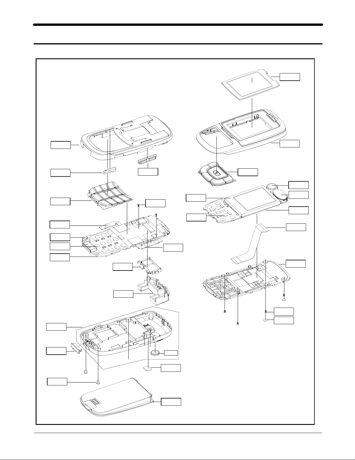
3. SGH-E630 Exploded View and its Parts list
1. Cellular phone Exploded View
QMW02
QFR01
QCK01
QKP01
QCA02
QMI01
QME01
QMP01
QRE01
QCA01
QAN02
QVO01
QCR05
QVK01
QLC01
QME02
QFU01
QKP02
QMO01
QSP01
QMP02
QPC01
QFL01
QCR26
QSC02
QIF01
QCR31
QCW01
QRF01
QBA21
3-1
SAMSUNG Proprietary-Contents may change without notice
This Document can not be used without Samsung's authorization

Exploded view and its Part list
2. Cellular phone Parts list
Location
NO.
QMW02 WINDOW LCD GH72-15021A
QFU01 MEC-SLIDE UPPER GH75-04606A
QKP02 KEYPAD SUB GH75-04612A
QMP02 LCD PBA GH92-01846A
QME02 LCD METAL DOME GH59-01438A
QFL01 MEC-SLIDE LOWER GH75-04607A
QSP01 SPEAKER 3001-001575
QMO01 MOTOR GH31-00098A
QLC01 LCD GH07-00561A
QCR26 SCREW MACHINE 6001-001850
QFR01 FRONT COVER GH75-04605A
QKP01 KEYPAD MAIN GH75-04611A
QIF01 IF CONN COVER GH72-15017A
QMP01 MAIN PBA GH92-01889A
QVK01 UNIT VOLUME KEY GH59-01436A
QME01 UNIT METAL DOME GH59-01437A
QCA02 UNIT CAM KEY GH59-01435A
QCR05 SCREW 6001-001478
QMI01 MICROPHONE ASSY GH30-00134A
QCK01 MEC CAM KEY GH75-04610A
QCR31 SCREW 6001-001795
QVO01 MEC SIDE KEY GH75-04609A
QRE01 MEC REAR COVER GH75-04608A
QRF01 RF COVER GH74-09508A
QBA21 BATTERY GH43-01447A
QPC01 PCB-FPCB GH41-00637A
QCA01 UNIT CAMERA GH59-01464A
QSC02 SCREW CAP GH74-11226A
QAN02 INTENNA GH42-00457A
QCW01 WINDOW CAMERA GH75-05299A
Description SEC CODE Remark
3-2
SAMSUNG Proprietary-Contents may change without notice
This Document can not be used without Samsung's authorization
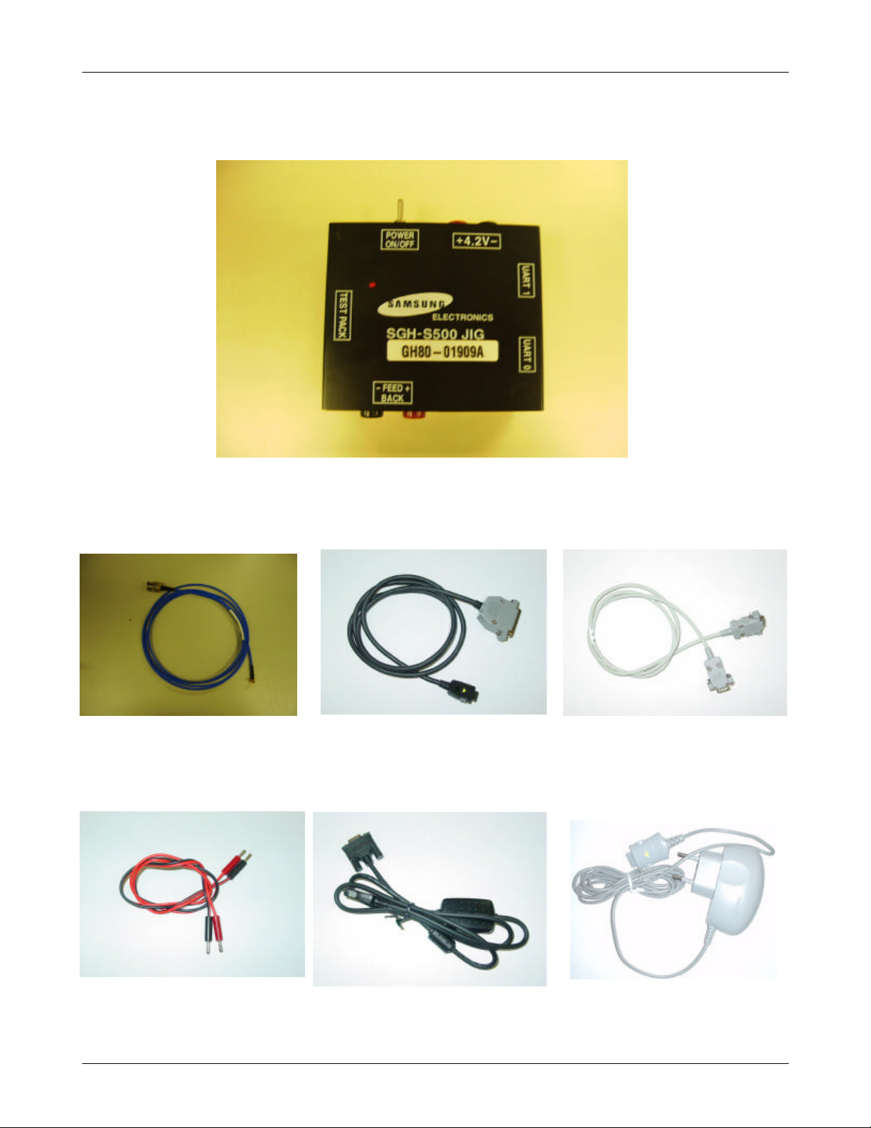
3. Test Jig (GH80-01909A)
Exploded view and its Part list
3-1. RF Test Cable
(GH39-00182A)
3-2. Test Cable
(GH39-00217A)
3-4. Power Supply Cable 3-5. DATA CABLE
(GH39-00219A)
3-3. Serial Cable
3-6. TA
(GH44-00483A)
3-3
SAMSUNG Proprietary-Contents may change without notice
This Document can not be used without Samsung's authorization

4. SGH-E630 MAIN Electrical Parts List
M A I N
SEC CODE Design LOC
0403-001387 ZD600
0504-000168 Q801
0504-001151 U206
0504-001151 U207
0506-000107 U801
0601-001790 LED700
0601-001790 LED701
0601-001790 LED702
0601-001790 LED703
0601-001790 LED706
0601-001790 LED709
0604-001261 U601
SEC CODE Design LOC
1405-001082 V601
1405-001082 V700
1405-001082 V701
1405-001082 V702
1405-001082 V703
1405-001082 V704
1405-001082 V705
1405-001082 V706
1405-001082 V707
1405-001082 V801
1405-001082 V802
1405-001082 V803
1405-001082 V804
0801-002237 U409
0801-002882 U301
0801-002882 U403
0801-002882 U405
1001-001253 U702
1203-003109 U602
1204-002138 U402
1205-002327 U100
1205-002350 U500
1404-001221 V600
1405-001082 V201
1405-001082 V202
1405-001082 V203
1405-001082 V204
1405-001082 V805
1405-001082 V812
1405-001082 V814
1405-001093 V503
1405-001093 V504
1405-001138 V808
1405-001138 V809
1405-001138 V810
2007-000138 R616
2007-000140 R125
2007-000140 R416
2007-000140 R700
2007-000141 R126
2007-000141 R303
1405-001082 V205
1405-001082 V501
1405-001082 V502
SAMSUNG Proprietary-Contents may change without notice
This Document can not be used without Samsung's authorization
2007-000141 R304
2007-000141 R412
2007-000141 R415
4-1

Electrical Parts List
SEC CODE Design LOC
2007-000141 R421
2007-000141 R708
2007-000143 R406
2007-000144 R736
2007-000145 R203
2007-000148 R108
2007-000148 R209
2007-000148 R210
2007-000148 R301
2007-000148 R312
2007-000148 R500
2007-000148 R706
2007-000148 R731
SEC CODE Design LOC
2007-000162 R615
2007-000162 R703
2007-000162 R722
2007-000162 R728
2007-000162 R801
2007-000171 R204
2007-000171 R207
2007-000171 R424
2007-000171 R429
2007-000171 R802
2007-000171 R803
2007-000171 R804
2007-000171 R805
2007-000157 R604
2007-000162 R300
2007-000162 R305
2007-000162 R306
2007-000162 R315
2007-000162 R407
2007-000162 R408
2007-000162 R410
2007-000162 R411
2007-000162 R413
2007-000162 R418
2007-000162 R425
2007-000162 R428
2007-000162 R600
2007-000171 R806
2007-000172 R727
2007-000172 R730
2007-000174 R122
2007-000566 R106
2007-000566 R107
2007-000566 R606
2007-000758 R605
2007-000982 R116
2007-000982 R117
2007-000982 R118
2007-000982 R119
2007-001301 R711
2007-001301 R712
2007-000162 R601
2007-000162 R602
2007-000162 R603
SAMSUNG Proprietary-Contents may change without notice
This Document can not be used without Samsung's authorization
2007-001301 R713
2007-001301 R714
2007-001301 R715
4-2
 Loading...