

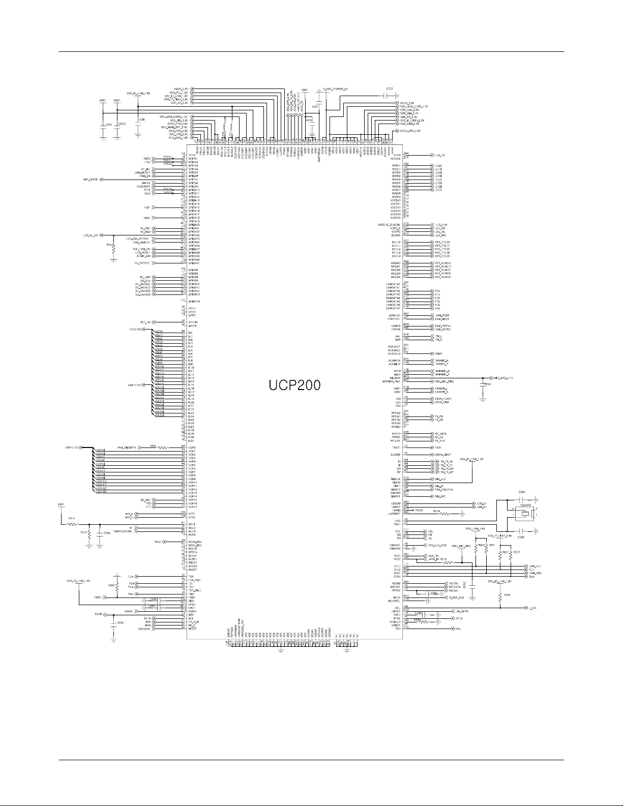
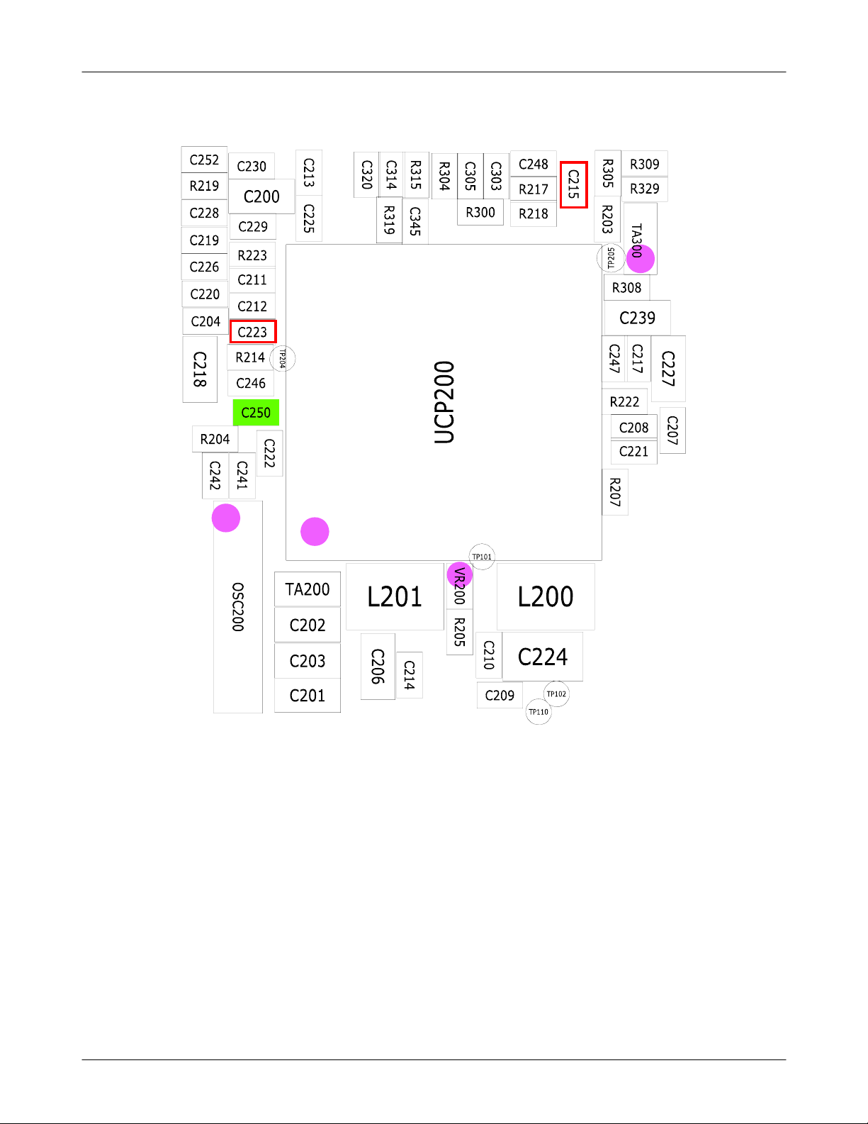
Page 1
9. Flow Chart of Troubleshooting
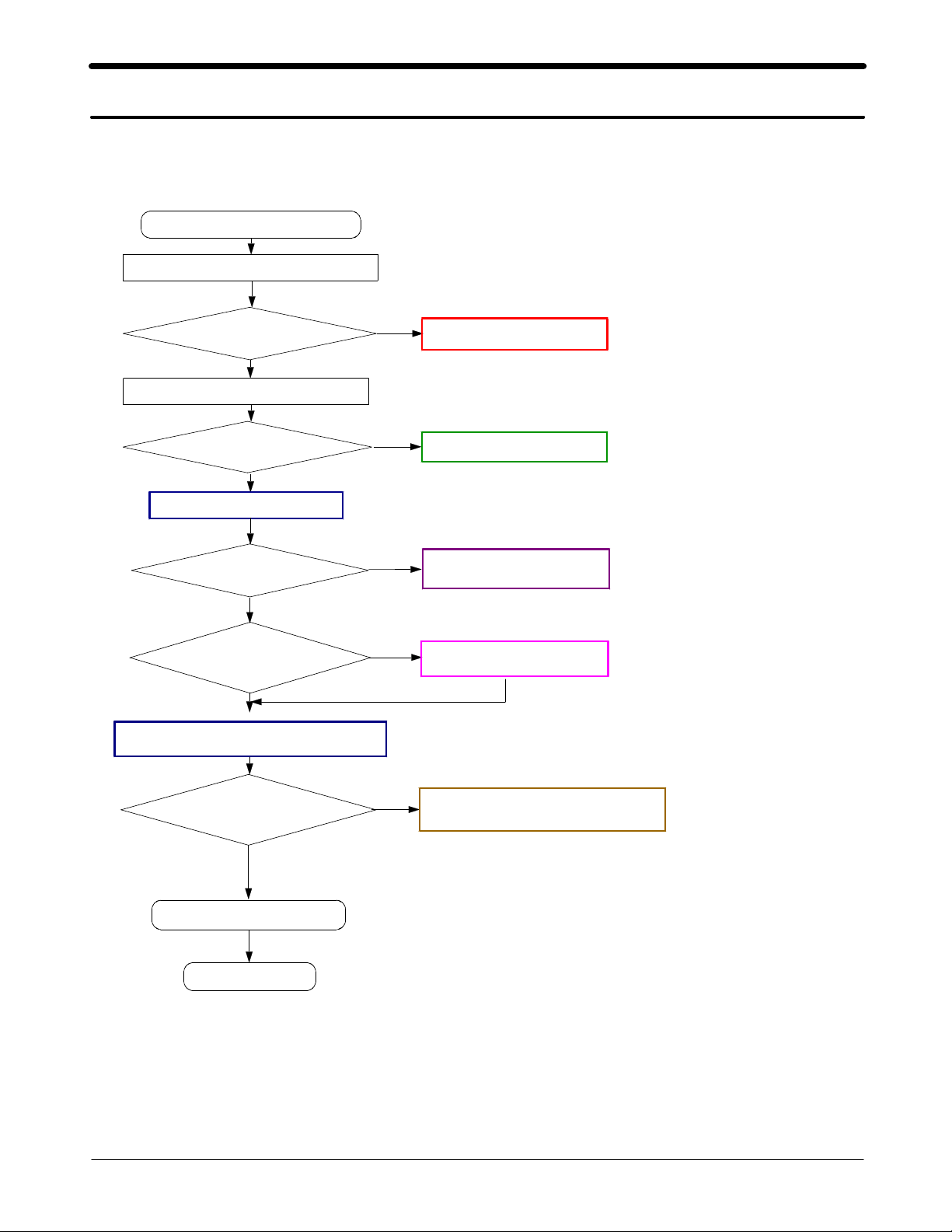
Baseband
9-1.
9-1-1.
Power ON
Power On' does not work
'
Check the current consumption
Yes
Current consumption
Check the Vbat Voltage
Voltage
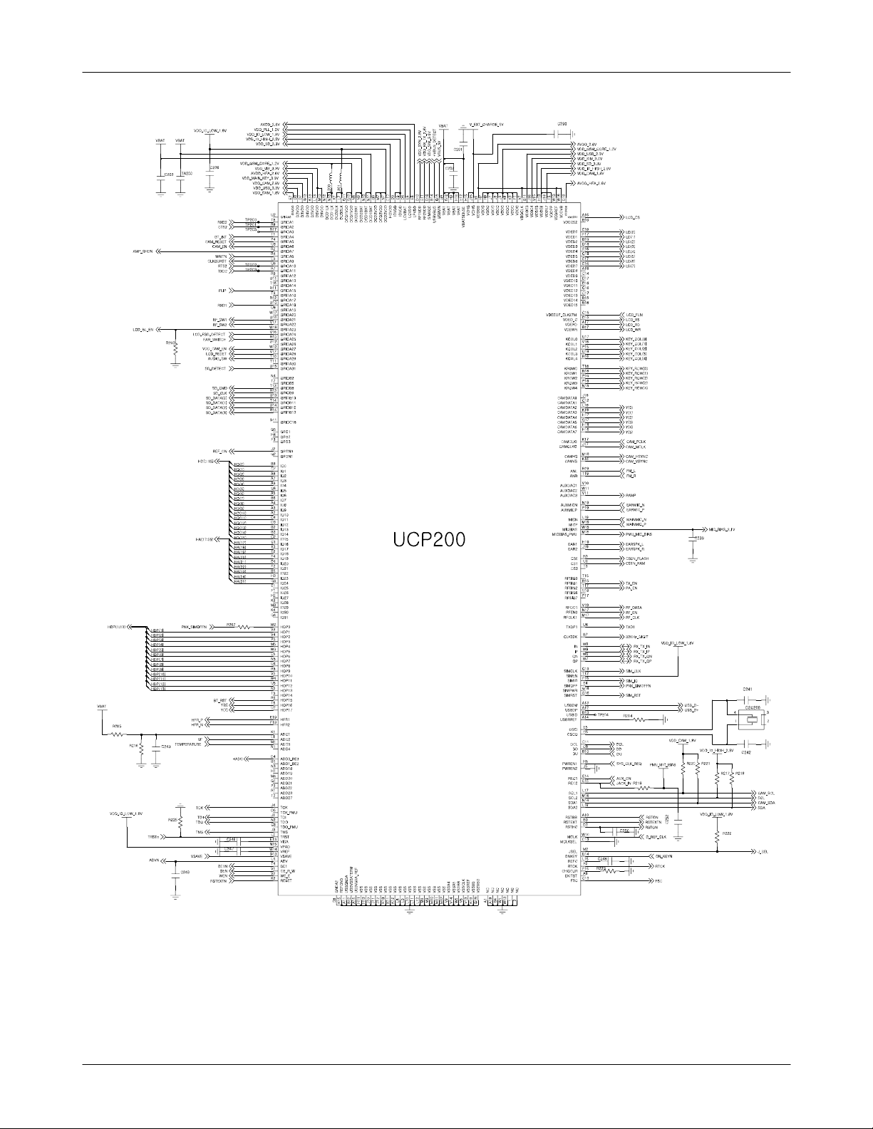
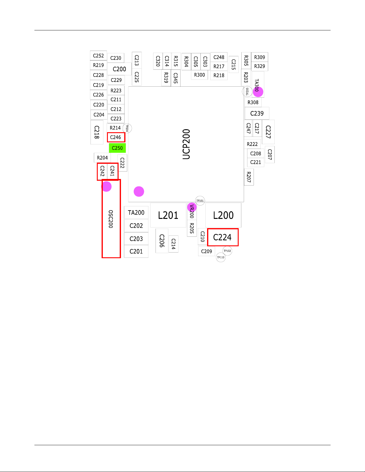
Check the pin of UCP200
C246(VISA)=
>= 100
mA
Yes
>=3.4V
Yes
2.5
Yes
V?
No
No
No
Download again
Charge the Battery
Check UCP200
C246
G11,G12(VDD_GSM_C
ORE)
Check the clock signal at OSC of PNX6608
Check the clock
Freq
Check the initial operation
=1.2
= 32.768k
Yes
END
V?
Yes
Hz
Yes
No
No
Check UCP200
C224
Check the clock generation circuit
relatedtoOSC2
(
C241, C242
00,
)
9-1
SAMSUNG Proprietary-Contents may change without notice
This Document can not be used without Samsung's authorization
Page 2
Flow Chart of Troubleshooting
9-2
SAMSUNG Proprietary-Contents may change without notice
This Document can not be used without Samsung's authorization
Page 3
Flow Chart of Troubleshooting
9-3
SAMSUNG Proprietary-Contents may change without notice
This Document can not be used without Samsung's authorization
Page 4
Flow Chart of Troubleshooting
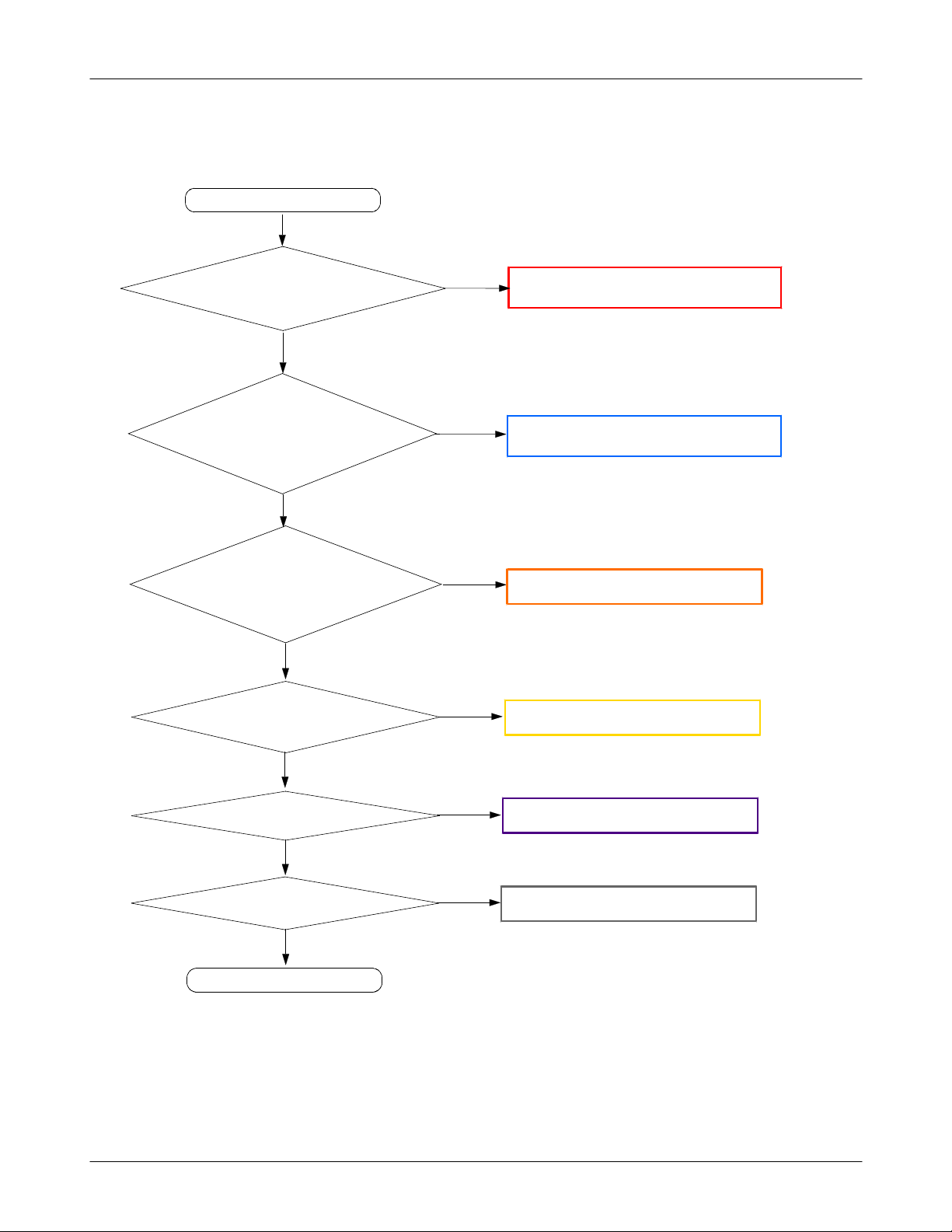
9-1-2.
Initial
Initial Failure
Yes
Is the RST Pin#A10(RSTON)
UCP200"Low→High"
of
Yes
The Pin
N8,N9,N10,N11(VBAT)
#
of PM300
There is
forms at the C241 and C242
>= 3.4V
Yes
kHz wave
32.768
of OSC200
No
?
No
-
No
Check the UCP200
if it has some problems,replace it
(
Check the UCP200
if it has some problems,replace it
(
Check the UCP200
.)
.)
Yes
The voltage is"High" at the
C215,C223
Yes
LCD display is O.K
Yes
Sound is O.K
Yes
END
No
No
No
Check the UCP200
Check the LCD part
Check the AUDIO part
9-4
SAMSUNG Proprietary-Contents may change without notice
This Document can not be used without Samsung's authorization
Page 5
Flow Chart of Troubleshooting
9-5
SAMSUNG Proprietary-Contents may change without notice
This Document can not be used without Samsung's authorization
Page 6
Flow Chart of Troubleshooting
9-6
SAMSUNG Proprietary-Contents may change without notice
This Document can not be used without Samsung's authorization
Page 7
Flow Chart of Troubleshooting
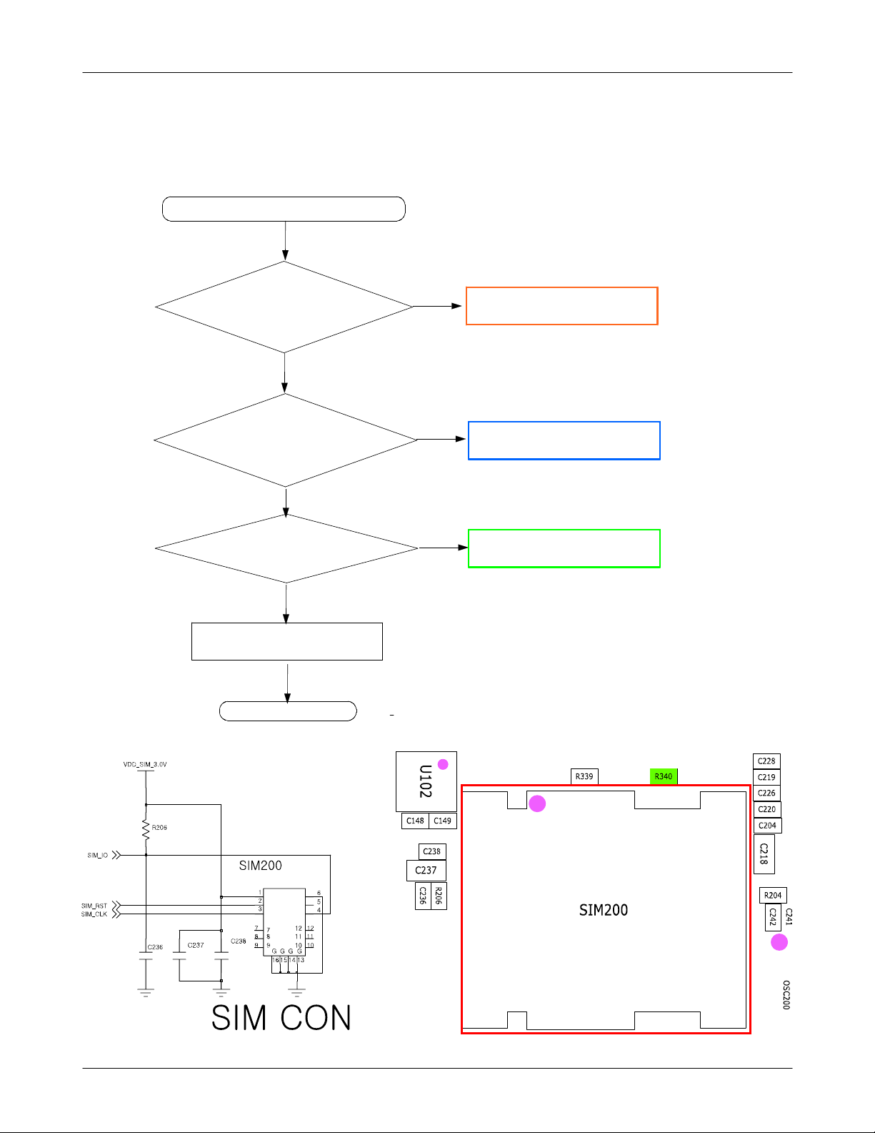
9-1-3.
Sim Part
Insert SIM is displayed on the LCD
"
Yes
SIM200 PIN#1
After Power On,
Check SIMCLK Signal On
PIN#3 of SIM200 inafew
After SIM Card insert,
SIM200 PIN#2="H"
=H?
Yes
second
Yes
No
No
No
Resolder or change UCP200
Check the clock
Replace PBA
Yes
Check the SIM Card
END
9-7
SAMSUNG Proprietary-Contents may change without notice
This Document can not be used without Samsung's authorization
Page 8

Flow Chart of Troubleshooting
9-1-4.
Microphone Part
Microphone does not work
Isthe Microphone
assembled correctly?
Check the reference voltage on mic path
Check the connection MIC
MIC_BIAS
Check mic-path connection
Yes
Yes
Yes
=2.1
Yes
V?
No
No
No
Resolderthe microphone
Resolder or replace
MIC300
Check UCP200
Resolder C317
END
Yes
9-8
SAMSUNG Proprietary-Contents may change without notice
This Document can not be used without Samsung's authorization
Page 9

Flow Chart of Troubleshooting
9-1-5.
Receiver/Speaker Part
There is no sound from the Receiver/Speaker
Yes
Is the terminal of
Receiver/Speaker O.K
Is there any signals at the
Pin#1and Pin#2of
SPK_PAD
Is there any signals at the
Pin#1and Pin#2of
SPK_PAD
?
Yes
?
Yes
Yes
No
No
No
Replace the Speaker
Check SPK_PAD
Check U306 PIN5,PIN
8
Is there any signals at the
Pin#1 and Pin#2 of
RCV_PAD
Yes
Is there any signals at the
E19,F19 of MODEM IC
Yes
END
No
No
Check RCV_PAD
Check UCP200
9-9
SAMSUNG Proprietary-Contents may change without notice
This Document can not be used without Samsung's authorization
Page 10

Flow Chart of Troubleshooting
9-1-6.
Charging Part
Abnormal charging part
What is the type of Charging?
Is the IFC300
V_EXT_CHARGE
Is the C200 Voltage
Yes
TA Charging
5V ?
≒
Yes
=H?
Yes
No
Check IFC300
No
Check UCP200
H15, J15 of UCP200
Yes
Check The Batte
END
=H?
ry
No
Check UCP200
9-10
SAMSUNG Proprietary-Contents may change without notice
This Document can not be used without Samsung's authorization
Page 11

Flow Chart of Troubleshooting
9-11
SAMSUNG Proprietary-Contents may change without notice
This Document can not be used without Samsung's authorization
Page 12

Flow Chart of Troubleshooting
9-1-7.
FM Receiver part
Abnormal FM part
What is the type of Charging?
Check the voltage at Pin
B6, F6
Is it OK?
Is there any signals at A5
of
U102?
Yes
TA Charging
of U102
Yes
A6,
No
No
Resolder or change U102
Resolder or change U102
Yes
Is there any signals at the
D6, E6 of
U102 ?
Yes
END
No
Check U102
or Resolder C148, C149
(
)
9-12
SAMSUNG Proprietary-Contents may change without notice
This Document can not be used without Samsung's authorization
Page 13

Flow Chart of Troubleshooting
9-2.
9-2-1.
RF
GSM
RX
900
Refer to the Line(GSM900 Rx path) in service schematic page1
*
Continuous Rx on, Rx input=-60dBm, Channel=
NORMAL CONDITION
catch the channel?
YES
RFS100 CHECK
Pin#
Insert Conduction RF cable)
(
PAM100 CHECK
Pin#
C103)
(
Pin#
C116)
(
dBm
2≥-65
dBm
-65
17 ≥
YES
F101CHECK
4 ≥
-65
dBm
YES
190
NO
NO
?
NO
?
NO
?
CHECK
ANT,C151,C100,C101
contact
?
RFS100
resolder or change
C103,C104,PAM100
resolder or change
C116,F101
resolder or change
U100 CHECK
Pin#
18,17 ≥
C118,C120)
(
OSC100 CHECK
Pin#
1, #3 : 26
Pad
(*
#1,3
C127,C128,C129
R105, C136
GSM
Receiver is OK?
900
END
YES
dBm
-65
YES
MHz
is visible)
YES
2.8V ?
V?
2.9
YES
NO
?
NO
NO
NO
C118,C120,L102
resolder or change
OSC100
resolder or change
C127,C128,C129,R105,C136
resolder or change
GSM
RX path component
900
resolder or change
s
9-13
SAMSUNG Proprietary-Contents may change without notice
This Document can not be used without Samsung's authorization
Page 14

9-2-2.
DCS1800 RX
Refer to the Line(DCS1800 Rx path) in service schematic page1
*
Flow Chart of Troubleshooting
Continuous Rx on, Rx input=-60dBm, Channel=
NORMAL CONDITION
catch the channel?
YES
RFS100 CHECK
Pin#
Insert Conduction RF cable)
(
PAM100 CHECK
Pin#
C103)
(
Pin#
C111)
(
Pin#
15,16 ≥
C110,C112)
(
dBm
2≥-65
dBm
-65
17 ≥
YES
F101CHECK
U100 CHECK
1 ≥
-65
dBm
YES
-65
YES
dBm
?
?
?
?
698
NO
NO
NO
NO
NO
CHECK
ANT,C151,C100,C101
contact
?
RFS100
resolder or change
C103,C104,PAM100
resolder or change
C111,F101
resolder or change
C110,C112,L101
resolder or change
YES
OSC100 CHECK
Pin#
1, #3 : 26
Pad
(*
C127,C128,C129
R105, C136
DCS1800 Receiver is OK?
#1,3
END
MHz
is visible)
YES
2.8V ?
V?
2.9
YES
NO
NO
NO
OSC100
resolder or change
C127,C128,C129,R105,C136
resolder or change
DCS1800 RX path component
resolder or change
9-14
SAMSUNG Proprietary-Contents may change without notice
This Document can not be used without Samsung's authorization
s
Page 15

Flow Chart of Troubleshooting
9-2-3.
GSM850 RX
Refer to the Line(GSM850 Rx path) in service schematic page1
*
Continuous Rx on, Rx input=-60dBm, Channel=
NORMAL CONDITION
catch the channel?
YES
RFS100 CHECK
Pin#
Insert Conduction RF cable)
(
PAM100 CHECK
Pin#
C103)
(
Pin#
C116)
(
Pin#
18,17 ≥
C118,C120)
(
dBm
2≥-65
dBm
-65
17 ≥
YES
F101CHECK
U100 CHECK
4 ≥
-65
dBm
YES
-65
YES
dBm
?
?
?
?
190
NO
NO
NO
NO
NO
CHECK
ANT,C151,C100,C101
contact
?
RFS100
resolder or change
C103,C104,PAM100
resolder or change
C123,F102
resolder or change
C118,C120,L102
resolder or change
YES
OSC100 CHECK
Pin#
1, #3 : 26
Pad
(*
#1,3
C127,C128,C129
R105, C136
GSM
Receiver is OK?
850
END
MHz
is visible)
YES
2.8V ?
V?
2.9
YES
NO
NO
NO
OSC100
resolder or change
C127,C128,C129,R105,C136
resolder or change
GSM
RX path component
850
resolder or change
9-15
SAMSUNG Proprietary-Contents may change without notice
This Document can not be used without Samsung's authorization
s
Page 16

Flow Chart of Troubleshooting
9-2-4.
PCS1900 RX
Continuous Rx on, Rx input=-60dBm, Channel=
Refer to the Line(PCS1900 Rx path) in service schematic page1
*
661
NORMAL CONDITION
catch the channel?
YES
RFS100 CHECK
Pin#
Insert Conduction RF cable)
(
PAM100 CHECK
Pin#
C103)
(
2≥-65
17 ≥
-65
dBm
dBm
YES
?
YES
?
NO
NO
NO
CHECK
ANT,C151,C100,C101
contact
?
RFS100
resolder or change
C103,C104,PAM100
resolder or change
F101CHECK
Pin#
C111)
(
U100 CHECK
Pin#
15,16 ≥
C110,C112)
(
OSC100 CHECK
Pin#
Pad
(*
C127,C128,C129
R105, C136
PCS1900 Receiver is OK?
-65
1 ≥
-65
YES
1, #3 : 26
is visible)
#1,3
YES
dBm
YES
dBm
YES
2.9
?
MHz
2.8V ?
V?
?
NO
NO
NO
NO
NO
C108,F100
resolder or change
C110,C112,L101
resolder or change
OSC100
resolder or change
C127,C128,C129,R105,C136
resolder or change
PCS1900 RX path component
resolder or change
s
END
9-16
SAMSUNG Proprietary-Contents may change without notice
This Document can not be used without Samsung's authorization
Page 17

Flow Chart of Troubleshooting
9-2-5.
GSM
850,
GSM
900
GSM850 MS:19PCL,
GSM900 MS:19PCL,38CH
Check RFS100
Pin
#2=2~5
Check and Change
C152,C100,C101
Main antenna
dBm
Yes
Check
190
TX
Refer to the Line(Low band Tx path) in service schematic page1
*
CH
No
PAM100 RF_SW1
Pin#5=LOW?
Yes
PAM100 TX_EN
Pin
#4 : 2.8V ?
Pad#4is visible)
(*
Yes
PAM100 VBAT
Pin
#30 :3.8V
C104)
(
Yes
No
No
No
Check UCP200 working
Check UCP200 working
Check C104
Checkbatteryblockworking
or
PAM100 PA_EN
Pin
Pad#2is visible)
(*
PAM100 VRAMP
Pin
Pad#3is visible)
(*
Check PAM100
Pin
(
#2="
#3 =
#27=-5
C119)
High"
Yes
High
Yes
Yes
END
dBm
No
No
?
No
Check UCP200 working
Check U100 working
Check C119
Check U100 working
or
9-17
SAMSUNG Proprietary-Contents may change without notice
This Document can not be used without Samsung's authorization
Page 18

9-2-6.
DCS
1800,
PCS1900 TX
Flow Chart of Troubleshooting
Refer to the Line(High band Tx path) in service schematic page1
*
GSM1900 MS:15PCL,
GSM1800 MS:15PCL,
Check RFS100
Pin
#2=2~5
Check and Change
C152,C100,C101
Main antenna
dBm
Yes
Check
660
700
CH
CH
No
PAM100 RF_SW1
Pin#5=High?
Yes
PAM100 TX_EN
Pin
#4 : 2.8V ?
Pad#4is visible)
(*
Yes
PAM100 VBAT
Pin
#30 :3.8V
C104)
(
Yes
PAM100 PA_EN
Pin
Pad#2is visible)
(*
PAM100 VRAMP
Pin
Pad#3is visible)
(*
#2="
#3 =
High"
Yes
High
Yes
No
Check UCP200 working
No
No
?
Check UCP200 working
Check C104
Checkbatteryblockworking
No
No
Check UCP200 working
Check U100 working
or
Check PAM100
Pin
C119)
(
#27=-5
END
dBm
Yes
No
Check L103,C125,C126
9-18
SAMSUNG Proprietary-Contents may change without notice
This Document can not be used without Samsung's authorization
Check U100 working
or
Page 19

Flow Chart of Troubleshooting
RF Schematic
9-19
SAMSUNG Proprietary-Contents may change without notice
This Document can not be used without Samsung's authorization
Page 20

RF Layout
Flow Chart of Troubleshooting
601CS501CS
C137
C129
O
S
C
1
0
0
R105
C133C134
C
1
0
4
C126
L103
C125
S
C
1
0
7
S
C
1
0
4
A
C136
P
C127 C128
F100
S
C
1
0
0
S
C
1
0
2
R
F
1
0
1
F102
C109
C105
C112
C110
C120
C118
C124
C121
F
C123
C116
C111
C108
C
1
0
6
L
1
0
1
L
1
0
2
C
1
2
2
C130
U
1
0
0
0
0
1
M
S
1
0
0
C
L
1
1
0
0
0
3
C119
SC103
C
C102
1
0
0
C101
C
1
5
2
9-20
SC101
SAMSUNG Proprietary-Contents may change without notice
This Document can not be used without Samsung's authorization
Page 21

Block Diagrams
7.
7-1
SAMSUNG Proprietary-Contents may change without notice
This Document can not be used without Samsung's authorization
Page 22

PCB Diagrams
8.
Main top view]
[
8-1
SAMSUNG Proprietary-Contents may change without notice
This Document can not be used without Samsung's authorization
Page 23

Main Bottom view]
[
PCB Diagrams
8-2
SAMSUNG Proprietary-Contents may change without notice
This Document can not be used without Samsung's authorization
 Loading...