Samsung SGH-E105 Service Manual
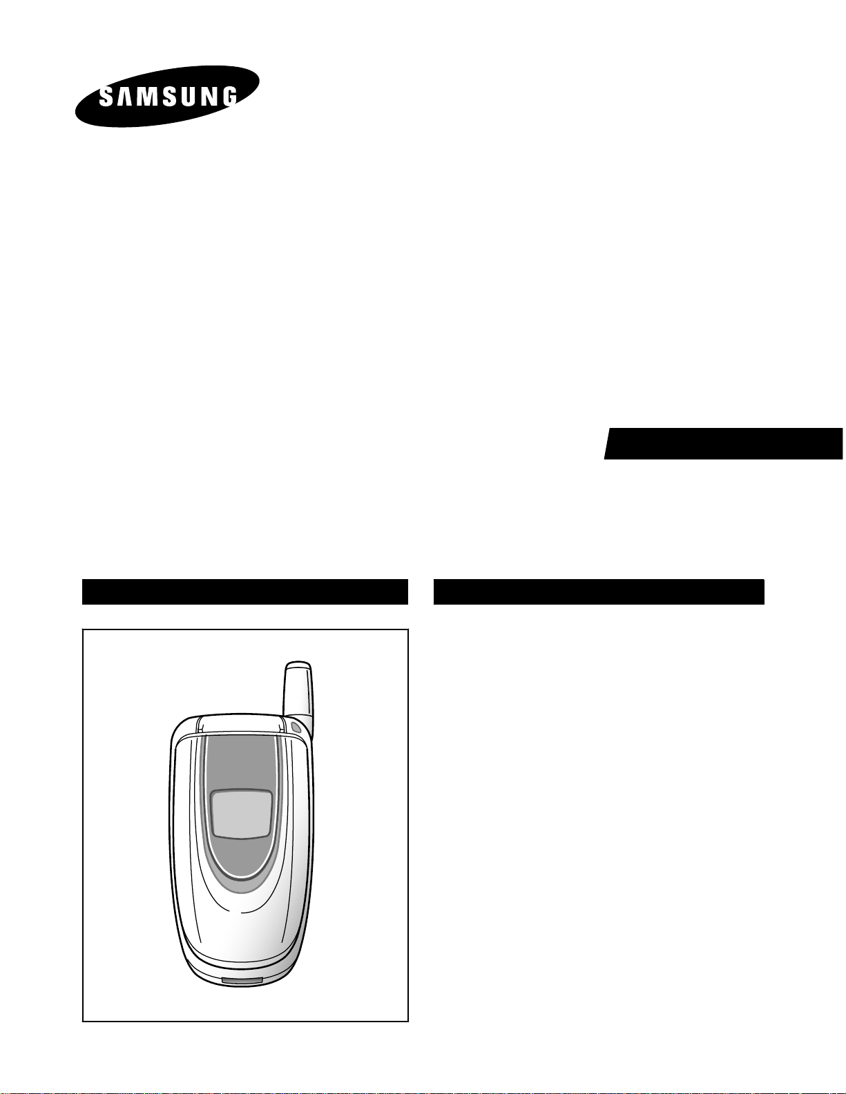
GSM TELEPHONE
SGH-E105
Manual
SERVICE
GSM TELEPHONE CONTENTS
1. Specification
2. Exploded Views and Parts List
3. Electrical Parts List
4. Flow Chart of Troubleshooting
5. Block Diagrams
6. PCB Diagrams

2. SGH-E105 Exploded View and its Parts list
1. Cellular phone Exploded View
10
1
2
11
18
19
12
13
14
15
16
17
3
4
5
7
8
9
6
20
21
22
2-1
SAMSUNG Proprietary-Contents may change without notice
This Document can not be used without Samsung's authorization
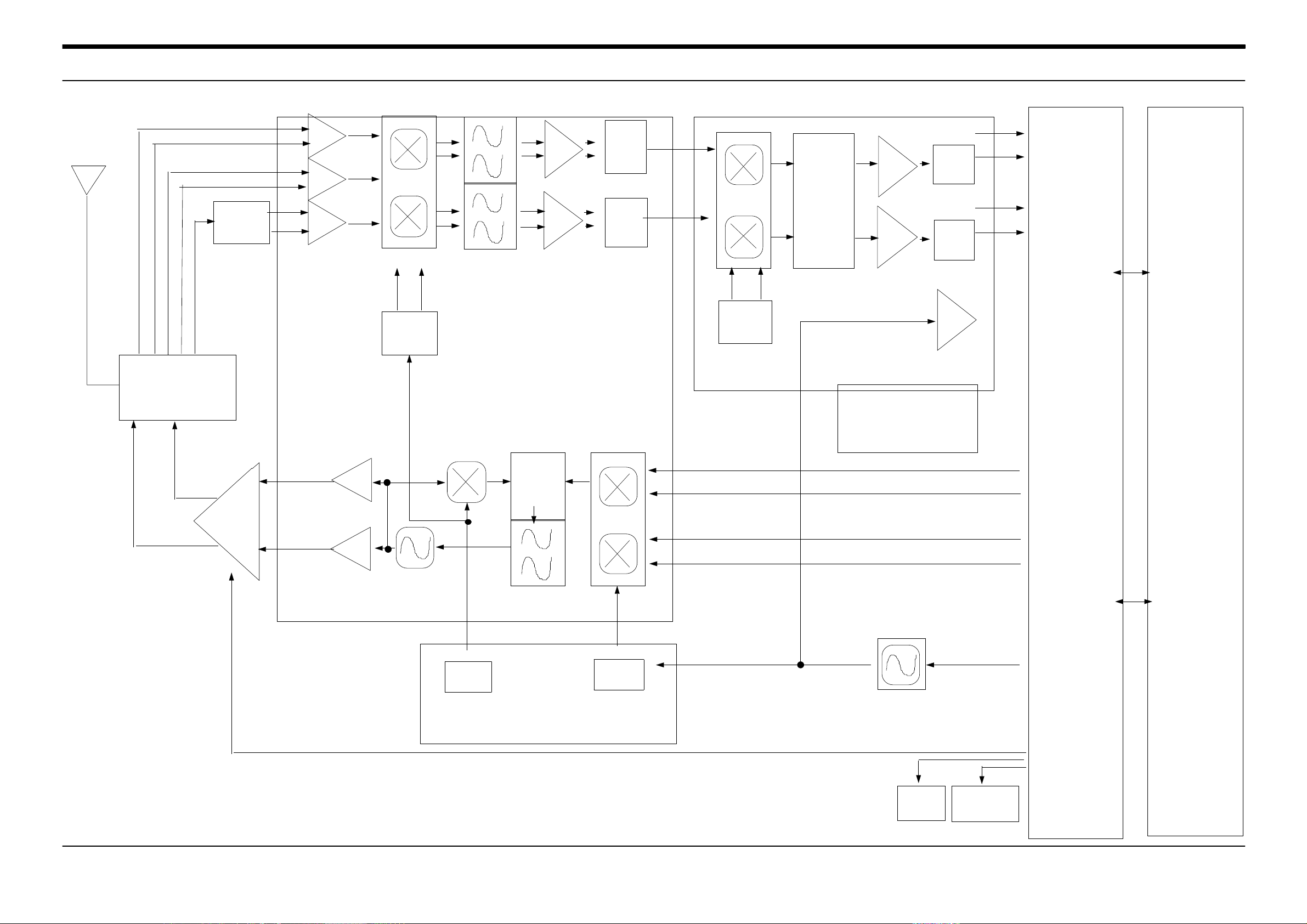
5. SGH-E105 Block Diagrams
1. RF Solution Block Diagram
Antenna
GSM:925MHz~960MHz
RF
FILTER
PCS:1930MHz~1990MHz
FEM
CSP1093
L
PGA
N
A
PGA
ADC
ADC
CHANNEL
FILTER
PGA
PGA
I
DAC
Q
DAC
TRIDENT
DSP16000
100KHz
1/2
SI4201
SI4200
SERIAL DATA
INTERFACE
BASE
BAND
GSM:890MHz~915MHz
PAM
PCS:1850MHz~1910MHz
TX VCO
RF
PLL
DET
SI4133T
IF
PLL
CLK
I
ARM7TDMI
Q
TCVCXO
13MHz
AFC
TXPOWER
5-1
SAMSUNG Proprietary-Contents may change without notice
This Document can not be used without Samsung's authorization
UI
AUDIO
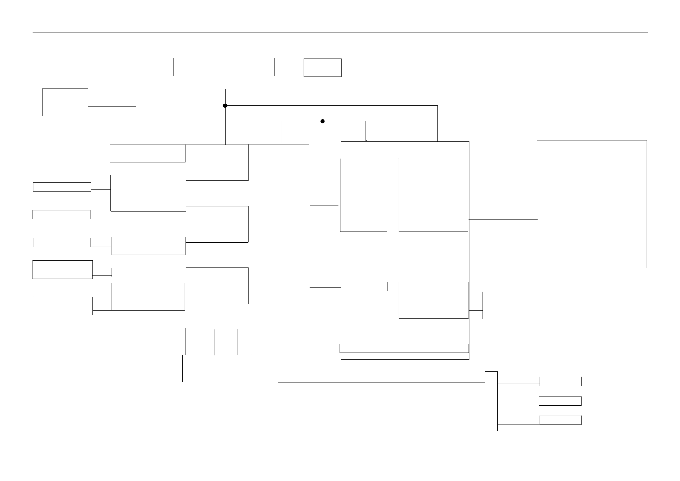
SGH-E105 Block Diagrams
2. Base Band Solution Block Diagram
IRDA
RS232
GPIO
SIM I/O
X-TAL
32.768 KHz
ARM
JTAG/ICE
TRIDENT
ACC
PPI
(Programmable
Peripheral I/O)
SMART
CARD
RTC
JTAG/ICE
POWER
(DC/DC, CHARGER)
DSP16000
ARM7TDMI
EMI
IO
RWN
AB(8:0)
DB(15:0)
INT1
IRQx
PAx
RSTB
DSPJTAG
LCD
KEYBOARD
X-TAL
13MHz
IO
RWN
AB(8:0)
DB(15:0)
INT1
IRQx
PAx
RSTB
JTAG
CSP1093
<RF DRIVER>
TX I/Q
RX I/Q
TXP
SERCK
SERLE
SERDA
OCTL
DAICK
DAIRN
DAIDO
DAIDI
DAI
TXIP
TXIN
TXQP
TXQN
RXIP
RXIN
RXQP
RXQN
SERCK
SERLE
SERDA
RXOVL
TXP
OCTL
RF SOLUTION
-RFIC
-PAM
MCP
128M FLASH
16M SRAM
Memory Part
AUDIO PART
AUDIO
LCD
MOTOR
B'D to B'D Connector
5-2
SAMSUNG Proprietary-Contents may change without notice
This Document can not be used without Samsung's authorization

4. SGH-E105 Flow Chart of Troubleshooting and Circuit Diagrams
1.Baseband
1. Power ON
'Power On' does not
work
Check the current
consumtion more than
100mA
YES
Check the
Vbat(battery+O)
Voltage more than
3.3V
YES
Check the pin
15 of U100 is more
than 2.8V
YES
U100 pin 46,39
=2.8V
NO
NO
NO
NO
Download again
Charge the Battery
Check U100 and C113
Check C114 and C116
YES
U100 pin 13
=1.8V
YES
Checktheclocksignal
at
pin4 of U800
Freq=13MHz ?
Vrms°√300mV ?
Vpp is around
900mVpp
YES
'Power On' does not
work
END
NO
NO
Check C112
Check the clock generation circuit
(related to OSC801 and U800)
4-1
SAMSUNG Proprietary-Contents may change without notice
This Document can not be used without Samsung's authorization
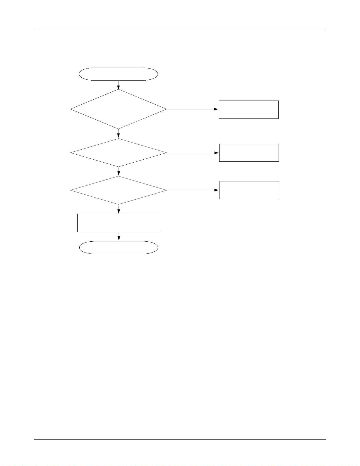
SGH-E105 Flow Chart of Troubleshooting and Circuit Diagrams
2. Initial
Initial Failure
Check the signal at the
pin28ofU100is
"High" when the phone
is boot on
YES
Check the pin 22 of
U100 is "High"
YES
Check the pin 4 of
OSC801 is around 2.8V
YES
Check and resolder LCD connector CN200
if there is solder bridhe between the pins
YES
END
NO
NO
NO
Check U100
Check the U700
Check the soldered status of
OSC801, R803, U100
4-2
SAMSUNG Proprietary-Contents may change without notice
This Document can not be used without Samsung's authorization
3. Sim Part
SGH-E105 Flow Chart of Troubleshooting and Circuit Diagrams
Phone can't access SIM card
Check the pin 1 of CN100.
Voltage = 3V?
YES
Check the SIM
connector's (CN100)
connector's to SIM card
YES
Check the circuit around CN100 input
circuitry
YES
Check the circuit around U601 output
and voltage supply circuitry
YES
END
NO
NO
NO
NO
Check the circuit related to
resolder or change CN100
Check the related circuit of
Check the related circuit of
U100
CN100
U601 and U100
4-3
SAMSUNG Proprietary-Contents may change without notice
This Document can not be used without Samsung's authorization
 Loading...