


SERVICE
GSM Mobile Cellular
Phone
SGH-600
4
5
6
GHI
JKL
MNO
7
8
9
PQRS
TUV
WXYZ
0
C
2
ABC
/OK
3
DEF
1
.
/
Manual
GSM Mobile Cellular Phone CONTENTS
1. General Description
2. Circuit Description
3. Specification
4. Manual Adjustment Test Procedure
5. Troubleshooting
6. PCB Views
7. Electrical Parts List
8. Exploded Views and Parts List
9. Block Diagram
10. Schematic Diagrams

Samsung Electronics Co.,Ltd.
ELECTRONICS

1. General Description
1-1 GSM System
1-1-1 Calls
GSM¨is an acronym for Global System for Mobile communications©, using TDMA for wide-area cellular
operation. The GSM system consists of the sub-systems shown;
The Mobile Station (MS) talks to the Base Station System (BSS) via an RF air interface. The Base Station System
(BSS) consists of Base Transceiver Station (BTS) and a Base Station Controller (BSC). The microwave link
between BTS and BSC is called an Abis interface. Generally one BSC controls 20 to 30 BTSs, and a Mobile
Switching Center (MSC) controlling the traffic among different cells would be reported back from a number of
BSSs. A Visitor Location Register (VLR) will be allocated to one MSC to find the mobiles out of their home cell
by listing them to VLR. The MSC would also be connected to the Home Location Register (HLR), the
Authentication Center (AC) and the Equipment Identity Register (EIR) So the system verify that the users and
equipment are legal subscriber.
1-1-2 Channels
Channels used in the GSM system can be divided into two classes - Logical and Physical channel. Physical
channels can be described in terms of their frequency and time domain characteristics. They are the actual
frequencies and timeslots the MS and BS transmits or receives on. The logical channels are mapped onto these
physical channels logically. Any particular and instant, physical channels may be control or traffic channels,
which determines the function of a physical channel at a particular point in time.
1-1-3 Airinterface of ARFCN (Absolute Radio Frequency Channel Number)
Samsung Electronics 1-1
1 2 3 ... ... ... ... ... 123 124
890.2 MHz 914.8 MHz
935.2 MHz
P-GSM: TX: Fl(n) = 890 + 0.2*n (1≤n≤124)
RX: Fu(n) = Fl(n) + 45
< Fig. 1 ARFCN Diagram >
959.8 MHz
1 2 3 ... ... ... ... ... 123 124

1-2 Samsung Electronics
General Description
1-1-5 Logical Channel
TCH (Traffic CH) is used mainly for transferring the speech information, and the BCH (Broadcast CH) is
related to control information.The major function of BCH is transferring information on the downlink for MS
synchronization, identification, paging, and controll. BCH is always radiated from every cells and the MS tries
to find the BCH which has highest level soon after turned on. The organization of BCH is shown belows;
FCCH (Frequency Correction Channel), SCH (Synchronization Channel), and BCCH (Broadcast Control
Channel). CCCH (Common Control Channel) will play a role like a message board, and is divided into two
control channels - PCH (Paging Channel) and AGCH (Access Grant Channel). SACCH (Slow Associated
Control Channel) exists every 12 frames, controlling and controls the TX power level and timing advance of
MS, transferring cell information to MS on downlink, transferring the information about RX level, Quality, and
RX level of adjacent cell on uplink. FACCH (Fast Associated Control Channel) steals and changes the TCH
when needing a Handover. SDCCH (Stand-alone Dedicated Control Channel) and RACH (Random Access
Channel) operate during the call setup procedure.
1-1-4 GSM TDMA Timeslots, Frames, and Multiframes
0 1 2 3 4 ... ... ... ... ... ... 24 25
TCH
Multiframe
0 1 2 3 4 ... ... ... ... ... ... 49 50
01234567
BCH
Multiframe
TDMA
Frame
T Information F Midamble F Information T Guard
Timeslot
< Fig. 2 Concept of Frames and Timeslots >

1-3Samsung Electronics
General Description
1-2 GSM HHP Feature
1-2-1 Main Set (HHP)
The main set is a microprocessor (KERNEL5)-controlled, full duplex radiotelephone system that provides the
user with GSM cellular service through cell sites linked to control centers.
It also provides functions related to frequency control, power control, and many user-convenience feactures.
1-2-2 Desktop Charger
The DTC is designed to charge batteries from commercial mains. The charger has two battery receptacles.
The forward one is for rapid charging, and the rear for normal charging.
1-2-3 Travel Adaptor
The travel adaptor is designed to operate the main set by supplying power to directly, while charging batteries
from commercial mains.
1-2-4 Cigar Lighter Adaptor
A cigar lighter adaptor is used to operate the main set and charger the battery from a 12 volt vehicular
electrical system.
1-2-5 Hands Free Car Kit
The Hands Free kit provides unlimited talk time, as power is supplied by the vehicular electrical system, and
improved receiving and transmitting due to the external antenna.
The Hands Free car kit adapts an external speaker, a hands-free microphone, a bracket, and a cradle for
mounting the main set. ¨Hands Free©means user can have a conversation without holding the phone by hand.

1-4 Samsung Electronics
General Description
MEMO

3. Specification
3-1 General Specification
3-1-1 Frequency Range
- Transmit (Uplink): 890 ~ 915 MHz
- Receive (Downlink): 935 ~ 960 MHz
3-1-2 Channel Spacing : 200 kHz
3-1-3 Number of Channels: 124
3-1-4 Frequency Spacing: 45 MHz
3-1-5 Modulation Data Rate
- 270.833 kbits/sec
3-1-6 Frame Period: 4.615 msec
3-1-7 Timeslot Period: 576.9 µsec
3-1-8 Modulation Type: 0.3 GMSK
3-1-9 MS Max Power: 2 W (33 dBm)
3-1-10 MS Min Power: 0.3 W (5 dBm)
3-1-11 Voice Coder Bit Rate: 13 kbits/sec
3-1-12 Input / Output Impedance : 50½
3-1-13 VCO Frequency
- TX VCO : 890 ~ 915 MHz,
- UHF VCO : 1160 ~ 1185 MHz
- VHF VCO : 540 MHz
3-1-14 IF
- 1st RX IF: 225 MHz
- 2nd RX IF: 45 MHz
- 1st TX IF: 270 MHz
3-1-15 VCTCXO Frequency
- 13 MHz (±5 PPM)
3-1-16 Operating Temperature
- Main : Nominal: +15 ¼C ~ +35 ¼C
Extreme: -10 ¼C (spec) ~ +55 ¼C
- TA : Nominal: +15 ¼C ~+35 ¼C
Extreme: -20 ¼C ~ +55 ¼C
3-1-17 Operating Voltage
- High Voltage: 4.1 V
- Nominal Voltage: 3.7 V
- Low Voltage: 3.4 V
Samsung Electronics 3-1
3-2 Transmitter Specification
3-2-1 Power
3-2-2 Power Ramping Time Level
The power-time template requirements for mobile
stations also apply to base stations. The only
difference is that, in the base station case, no short
burst (random access) exists. To measure the
template, the base station has to be operated in its
bursting mode. This test cannot be performed on the
base channel, since a base station has to transmit
continuously in all time slots. In most cases, an
additional channel besides the base channel has to
be activated or the transmitter under test is not
considered to be configured as a base channel
transmitter. The average peak power from the
previous part of the test is used as a reference. The
time reference is provided by the training sequence
in the middle of the burst. The template has to meet
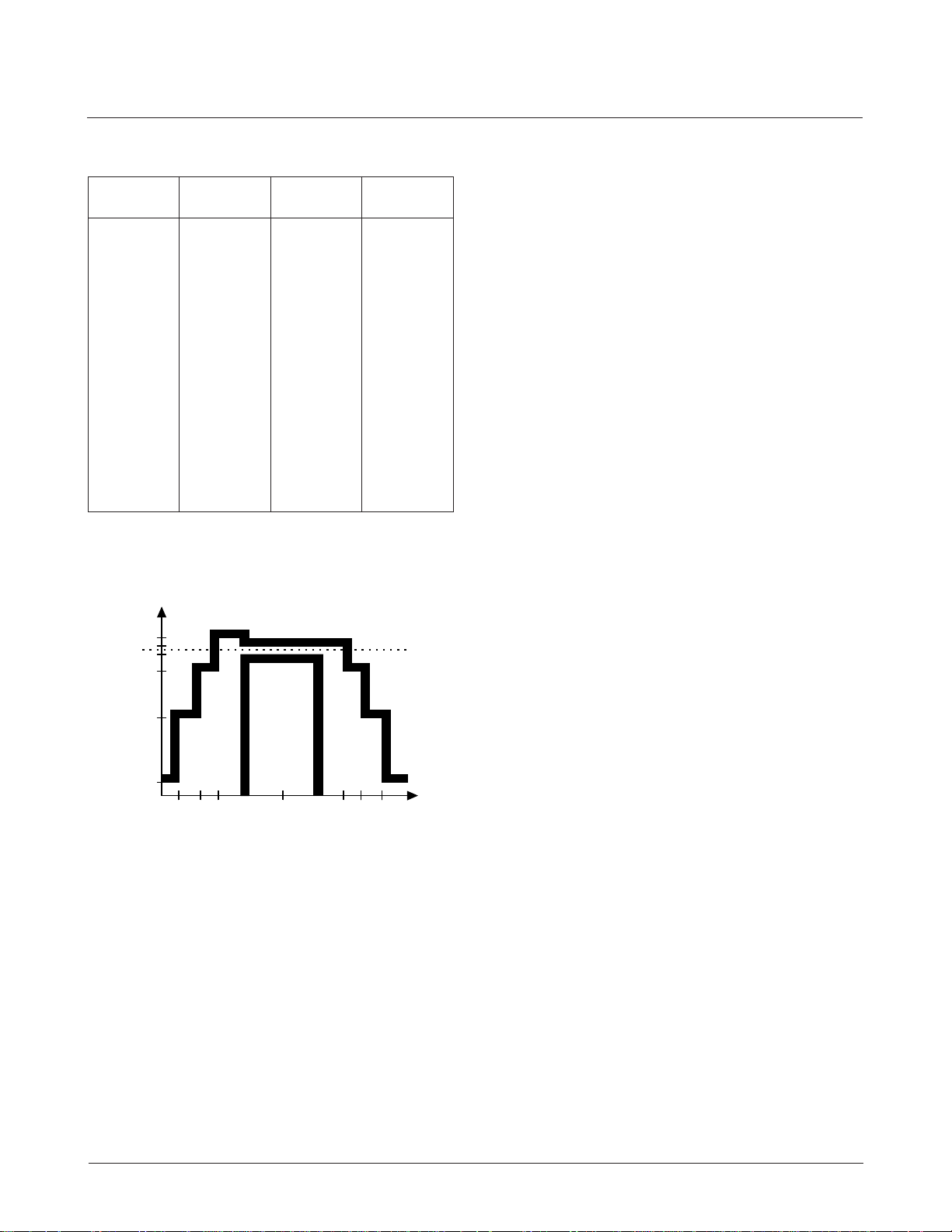
the requirements of Fig. 6. Again, the noise level of 70 dBc is dependent on the actual transmitted
power level. If this level is below -36 dBm, the
absolute level applies. The template is usually
evaluated along with the peak power level.
3-2-3 IF Filter
- 270 MHz LC Filter
3-2-4 TX SAW Filter
- Spurious signal atenuating : ²-70 dBc
- Wide Bandwidth to make plane Group delay
characteristic
3-2-5 Power Amplifier
- Total Efficiency: 40~45 % at Pin=1mW,
VDD=3.6 V, Pout=3.2 W
Power Peak Norminal Extreme
Control LevelPower (dBm) (dB) (dB)
5 33 ±2 dB ±2.5 dB
6 31 ±3 dB ±4 dB
7 29 ±3 dB ±4 dB
8 27 ±3 dB ±4 dB
9 25 ±3 dB ±4 dB
10 23 ±3 dB ±4 dB
11 21 ±3 dB ±4 dB
12 19 ±3 dB ±4 dB
13 17 ±3 dB ±4 dB
14 15 ±3 dB ±4 dB
15 13 ±3 dB ±4 dB
16 11 ±5 dB ±6 dB
17 9 ±5 dB ±6 dB
18 7 ±5 dB ±6 dB
19 5 ±5 dB ±6 dB
3-2 Samsung Electronics
Specification
dBc
+4
+1
0
-1
-6
-30
-70
10 8 10 TO
(147 bits)
10 8 10
[µs]
< Fig. 6 Power-Time Template >
Samsung Electronics 3-3
Specification
3-3 Synthesizer Specification
3-3-1 General Specification
- Frequency Hopping : 1 Channel to < 3orms in
< 500 mS
- Phase Noise: < 3o RMS
3-3-2 IF Synthesiser
- Synthesizer Frequency: 540 MHz
- Output Signal Drive Level: -10 dB
- 2nd IF LO Output Frequency FIR: 45 MHz
3-3-3 FIR Output
- 1st IF: 225 MHz
- 2nd IF: 45 MHz
- FIR Frequency: 45 MHz
- FIR Level: -17 dBm
3-3-4 Phase Noise Specification
3-4 Receiver Specification
3-4-1 Front-end Specification
- Input Frequency range: 935 MHz ~ 960 MHz
- Gain: 18 dB
- If Frequency range: 540 MHz
- Input Impedance: 150 ½
- Output Load: 1 k½
- Overall Sensitivity: -106 dBm for 9 dB S/N
in 180 kHz
3-4-2 Sensitivity
- Reference Sensitivity Level: -102 dBm
- Channel Width : 180 kHz
- Input Thermal Noise: -121.4 dBm/Hz
- Ouput S/N: > 9 dB
- Noise Figure: < 7 dB
3-4-3 Intermodulation
- Input Useful Signal: -99 dBm
- Interferer: -49 dBm at ± 800 kHz and 1600 kHz
3-4-4 Selectivity
Offset (kHz) Phase Noise (dBc/Hz)
± 200 < -75
± 250 < -78
± 400 < -105
> 600 < -105
> 1200 < -105
> 1800 < -113
> 3000 < -115
> 6000 < -121
> 10.0 MHz < -124
> 20.0 MHz < -129
> 30.0 MHz < -134
Signal Type Level
Useful Signal GMSK - 82 dBm
Cochannel GMSK - 9 dBc
± 200 kHz GMSK + 9 dBc
± 400 kHz GMSK + 41 dBc
± 600 kHz GMSK + 49 dBc

3-4 Samsung Electronics
Specification
MEMO

2. Circuit Description
2-1 RF Part
2-1-1 Frequency Generator
The 13MHz reference clock (VCTCXO) drives the logic and RF part. The 13 MHz reference is controlled by the
logic (10bits DAC minimum) and is kept to a frequency error less than ±0.1 ppm after synchronization with the
GSM network.
A 540 MHz oscillator is divided by 2 to generate a fixed 270 MHz VHF LO used in the TX I,Q modulator and
mixed by 270 MHz. The UHF LO for the first RX down conversion and the TX offset mixing works in
superheterodyne mode to reduce the relative bandwidth and to be able to work at a frequency greater than 1
GHz.
2-1-2 Transmitter
The baseband GSM chipset (Kernel5) generates I and Q baseband signals for the transmit vector modulator.
The modulator provides more than 40dBc of carrier and unwanted side-band rejection and produces GMSK
modulated signal, the ÔreferenceÕ signal at 270 MHz which passes to the offset phase-locked loop block (OPLL).
The OPLL consists of a down-converter, phase detector, loop filter and transmit VCO operating at the final RF
output frequency. The down converter mixes the UHF LO (eg. 1172 MHz) with the transmit VCO signal to
generate a ÔfeedbackÕ signal at 270 MHz. The ÔfeedbackÕ signal passes via a limiter to one port of the phase
detector. The GMSK ÔreferenceÕ signal from the vector modulator passes via a second limiter to the other input
port of the phase detector. The phase detector generates an error current proportional to the phase difference
between the ÔfeedbackÕ signal from the down-converter and the ÔreferenceÕ signal from the vector modulator.
This error current is filtered by a second order low-pass filter to generate an output voltage which depends on
the GMSK modulation and the desired channel frequency. This voltage controls the transmit VCO such that the
VCO output signal, centered on the correct RF channel, is frequency modulated with the original GMSK data.
The centre frequency of the transmit VCO is offset from the UHF LO frequency by 270 MHz. The OPLL acts as
a tracking narrowband band pass filter tuned to the desired channel frequency. This reduces the wideband
noise floor of the modulation and up-conversion process and provides significant filtering of spurious
products. The OPLL architecture results in a low-noise GMSK modulated signal at 902 MHz with very low
spurious content.
The RF GMSK output from the transmit VCO is fed via TX SAW filter to the RF power amplifier. The peak
output power and the profile of the transmitted burst are controlled by means of a closed feedback loop. The
RF output from the PA is sampled with a directional coupler. The sampled signal passes to an RF detector
diode whose output voltage is dependent on the incident RF level. This ÔfeedbackÕ voltage passes to the
inverting input of the loop integrator. A ÔreferenceÕ signal is generated within the baseband section under
control of the layer 1 software. The loop maintains zero difference between the ÔfeedbackÕ signal and the
ÔreferenceÕ signal. In this way, the amplitude and shape of the transmitted RF burst may be controlled by the
baseband processor. In particular, the rise and fall profiles can be controlled to meet the stringent power/time
templates and switching transient requirements of GSM 05.05.
The RF output passes to the antenna connector via an integrated TX/RX switch and lowpass filter to attenuate
the harmonics generated by the power amplifier.
Samsung Electronics 2-1
2-2 Samsung Electronics
2-2 Baseband Part
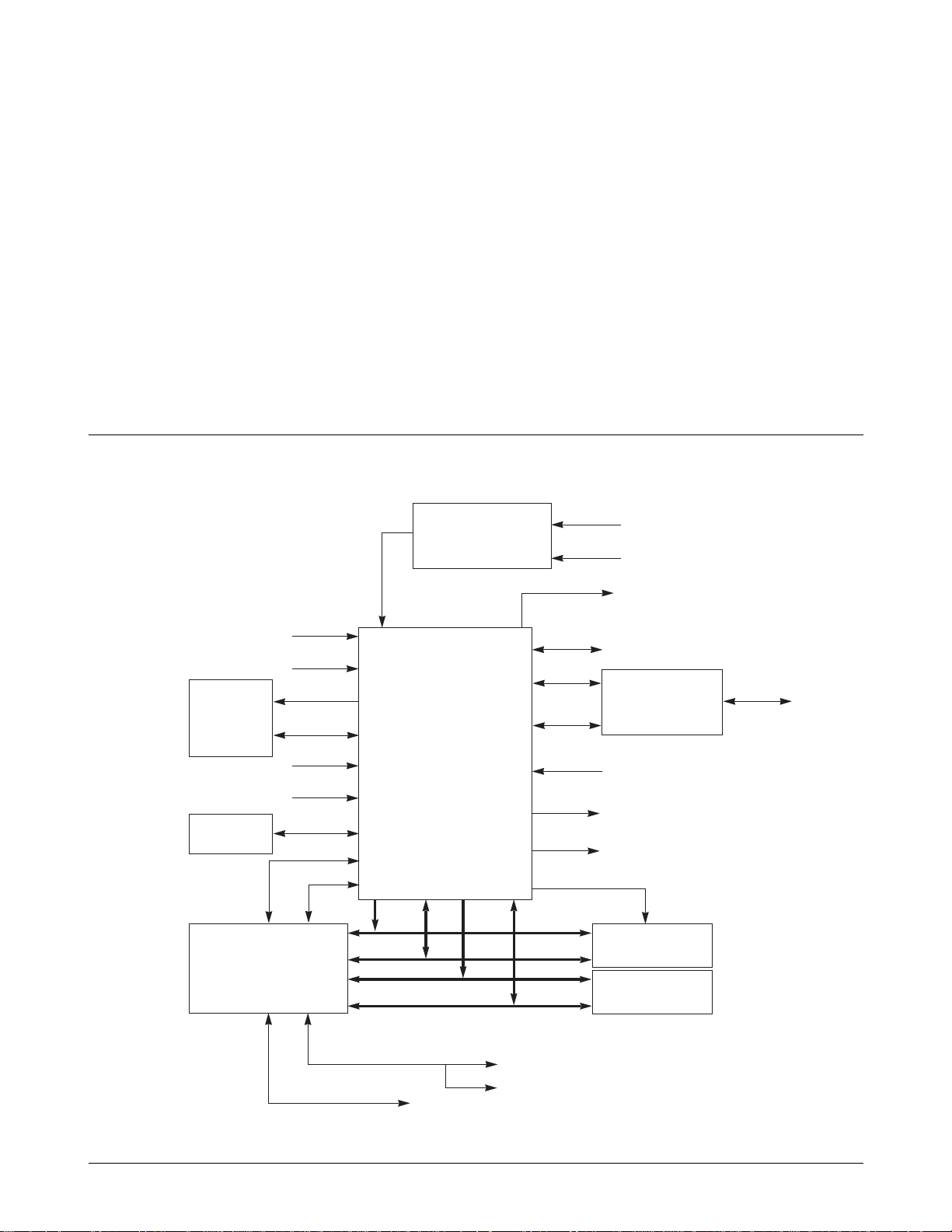
2-2-1 General Block Diagram
Circuit Description
cmd
cmd
cmd
cmd
power
clk
I,Q Rx
Vmid
I,Q Tx
RS232
3V/ 5V
add
data
add
data
audio
Earphone (Spk/Mic)
Spk/Mic
Vther.
Vcel.
dai
synth.cmd
radio.cmd
keyboard
Vib
voice data
eepdata
KERNEL
B.B. FILTER
SERIAL
EEPROM
VIBRATOR
SIM
TRANSLATOR
MEMORY
(Flash1 + SRAM)
Flash2
(Voice recognisation)
VOCODER
SIM I/F
SIM
2-1-3 Receiver
The incoming RF signal passes through the integrated lowpass filter and TX/RX switch. This is followed by a
947 MHz SAW Band Pass Filter and a bipolar low-noise amplifier (LNA). The HD155101BF includes an active
bias circuit which stabilizes the DC operating point of the LNA. The RF signal passes via a second RF SAW
filter to the first receive mixer. This mixer is implemented as a Gilbert cell within the HD155101BF. The
incoming signal at 947 MHz mixes with the UHF LO at 1172 MHz to generate a 225 MHz IF signal. The IF
signal passes from the mixer output via a 225 MHz IF SAW filter to the first IF amplifier. A further internal
Gilbert cell mixes the 225 MHz IF signal down to the 45 MHz second IF. The 45 MHz output from the second
mixer is filtered and passes to the AGC amplifier. The gain of the AGC amplifier is set by a DC control voltage
supplied by the baseband. The usable control range is in excess of 80dB. Finally, the AGC output signal at 45
MHz passes to the demodulator and is mixed down to DC to generate I and Q baseband signals. The baseband
signals pass via baseband filter to the baseband A/D converters. The remainder of the channel filtering is
performed by the baseband chipset.
(Voice recognition)
< Fig. 3 Baseband Block Diagram >

Samsung Electronics 2-3
2-2-2 ROM1 & SRAM
8M (X16) Flash ROM and 2M (X8) bit SRAM are used. Two devices are merged in one package. This device is a
combination memory organized as 524, 288 x 16 bit flash memory and 262, 144 x 8 bit static RAM in one
package.
2-2-3 ROM2
A 8M (X16) bit Flash Memory is used for the voice recognition and voice memory. This device is an 8, 388, 608
bit flash memory with batch chip erasing, sector erasing, and byte and word writing using a single 3V power
supply.
2-2-4 EEPROM
The kernel requires some external non-volatile memory to store various system parameters, such as RF control
calibrations, extra dial stores etc. A 64 K (65, 536) bit device is used. This device is internally organized 8192 x 8.
This device features a serial interface and software protocol allowing, operation on a simple, two wire bus.
2-3 SIM
2-3-1 SIM Interface
An interface is provided to a serial port controlling the SIM interface. It can support 5V and 3V SIM interface.
The hardware interface consists of SIMVCC, SIMdata I/O, SIMclk output, SIMRST output, and SIMPRES input.
The interface is controlled through TX Data, RX Data, control, and status registers. Transmit and receive data
may use a 256 byte buffer or be exchanged through single byte registers. SIMVCC may be used to control the
power supply to the SIM card.
Circuit Description
2-4 Samsung Electronics
2-4 POWER MANAGEMENT
2-4-1 DC/DC Converter
Our 1 cell Li-ion battery solution requires a up-converting DC/DC conversion circuit for efficiency
improvement. The device is a PWM Step-up DC/DC converter IC. Specification is as below;
¥ Vin: 2.75 V ~ 4.2 V
¥ Vout: 3.3 V ~ 4.1 V
¥ Ripple: less than 50 mVpp
¥ Efficiency: typ. 85 % (up to 96%)
2-4-2 Charger Circuitry
The simplified built-in charger circuit diagram is as below ;
Circuit Description
< Fig. 4 Built-in Charger Circuitry >
V DECTECTOR
DC
T DECTECTOR
DC IN DECTECTOR
BAT_VOLT
Buzzer
3.6V
3.3V
3.3V
3.6V
3.0V
3.0V
Temperature
DC In
Charger On
SCL
SDA
Vibrator
Backlight LED
CHARGER
B.B
DC/DCBATT
R.F
PAM
RTC
LDO
LDO
LDO

Samsung Electronics 2-5
2-5 RADIO INTERFACE
2-5-1 RF Block Diagram
2-5-2 Baseband Filter
To control the spectral splatter and thus the intersymbol interference (ISI), filtering is applied to the baseband
pulses. The required filtering achieved very simply using a small, low cost discrete LC structure, which has the
great advantage of not consuming current.
Circuit Description
LNA
RX SAW
RX SAW
IF
SAW
225 MHz
45 MHz
LC FILTER
÷6
HARMONIC
FILTER
TX/RX SWITCH
ANTENNA
SOCKET
947 MHz
270 MHz
Active Bias
HD 155101BF BRIGHT
270 MHz
902 MHz
540 MHz
45MHz
270 MHz
÷2
OPLL LOOP
FILTER
TX SAW
POWER
AMPLIFIER
RAMP DAC
DETECTOR
POWER CONTROL LOOP
I
AGC
DAC
Q
I
Q
AGC AMPLIFIER
IQ
DEMOD
IQ
MOD
90
o
SHIFT
÷2
90
o
SHIFT
÷2
PHASE
DET.
TX
VCO
VHF
VCO
UHF
VCO
13
MHz
AFC
DAC
1172 MHz
DUAL
SYNTH
RF
Buffer
< Fig. 5 RF Block Diagram >

2-6 Samsung Electronics
2-6 AUDIO
2-6-1 Audio Inputs
The Handset provides two audio inputs:
¥ Built in microphone
¥ Connection for external microphone
A microphone biasing amplifier reduces component count in the overall system design:
¥ Supply: 2.2 V regulated to ±20 %
¥ Different output to eliminate possible coupling noise problems, MICBIASP and MICBIASN
¥ Maximum current: 500 uA
¥ Maximum load: 200 pF
2-7 EXTERNAL INTERFACE
A 18 pin connector is mounted on the bottom corner of the PCB. The antenna external connection is on the
right hand side of this connector.
2-8 KERNEL SPECIFICATION
2-8-1 FEATURES
¥ Complete Layer 1 support
¥ TDMA burst building (ETSI Rec.5-02)
¥ Coding and interleaving (Rec. 5-03)
¥ GMSK with differential coding (Rec. 5-04)
¥ Programmable power template for Tx burst control
¥ AGC in Receive mode
¥ I,Q inputs or single intermediate frequency (IF) input
¥ Detection of FCCH, SCH, Normal and Dummy Bursts
¥ Flash ROM programming abilities
¥ Auxiliary ADC for battery voltage and temperature monitoring
Circuit Description

Samsung Electronics 2-7
2-8-2 Equalizer
MAJOR FEATURES
¥ Frequency Correction Burst Correction
¥ Frequency Correction Burst Frequency Measurement
¥ Synchronization Burst Long Preamble Correlation
¥ Normal Burst Short Preamble Correlation
¥ Channel Impulse Response Generation
¥ Possible Received Value Generation
¥ Data Equalization
¥ Carrier Power Measurement
¥ Doppler Shift Measurement and Correction
¥ Scaled 7-Bit Soft Decision
¥ I and Q component recovered from Received Data
2-9 VOCODER SPECIFICATION
2-9-1 FEATURE
¥ Complete GSM voice encoding and decoding functions
¥ DTX function
¥ Voice Activity Detection (VAD) output
¥ Fully asynchronous coding and decoding
¥ A-law PCM conversion
¥ DTMF generation
¥ Sidetone level control
¥ Programmable microphone amplifier with two differential input ports
¥ Two programmable audio output amplifiers
¥ 13 MHz master clock
Circuit Description

2-8 Samsung Electronics
2-10 Desk Top Charger
2-10-1 Charging
The desk-top charger contains switching regulator to charge a lithium battery from an DC/DC adaptor. The
battery type is detected at pin 15 (MPU) through U5 ( front port) and U26 (rear port). Battery charging current
is turned into Vi. Vi is measured at pin 12 (MPU) after R32 and C23 to cancel the noise. When the battery
voltage is too low, the charging circuit turns to trickle mode using Q9 and Q11.
2-10-2 Control Part
This circuit contains 4-bit micro controller (U21), including an I/O port, timer, A/D converter to control battery
charging. This circuit uses a 4 MHz main clock and +5V power.
BATTERY VOLTAGE DETECTION
Battery voltage from the front port is detected at R20, R18 and measured at pin 13 (MPU).
Battery voltage from the rear port is detected at R14, R13 and measured at pin 14 (MPU).
BATTERY TEMPERATURE DETECTION
The charger always detects the battery temperature via NTC thermistor to prevent battery thermal problems.
This circuit is composed of parallel resistors because NTC thermistor has log-scale thermal characteristics. If the
battery temperature exceeds 55 degrees C, charging stops.
AUTONOMOUS TIMER
If MPU has stopped charging and the timer goes to the ÔonÕ state by an external shock, overcharging may occur.
A timer (U7-4) prevents the battery from being overcharged by any unexpected external influence.
Circuit Description

Samsung Electronics 2-9
2-11 Cigar Lighter Adaptor (CLA)
2-11-1 General Description
The CLA is a regulated switched-mode power supply designed for use with a portable HHP. The power supply
is connected directly to the phone and provides a voltage path for charging a battery installed in the hand-held
portable phone.
2-11-2 Circuit Description
The input voltage range of CLA is from 12 Vdc to 30 Vdc, and the nominal voltage is 13.7 Vdc. The output
current is 600 mA. The ripple and noise amplitude is less than 50 mV at the input (12 V ~ 30 Vdc). And the
limit settings are shown below;
- Current limit : 600 mA ± 50 mA at nominal input 13.7 V
- Output voltage : 9.0 V (+/- 0.8 V) Vdc at no load.
In addition, the temperature limit is -20 upto +85 ¼C for storage, and 0 to +40 ¼C for operating. The CLA size of
SGH-600 is 89.3 x 43 x 27 mm, and the weight is 110 g.
2-12 Travel Adaptor (TA)
2-12-1 General Description
This adaptor is designed for use with a portable hand held phone (HHP). It is a switching-mode power supply
connected directly to the phone with a cable, and it provides a voltage for charging a battery installed in the
hand held portable phone.
2-12-2 Circuit Description
The input voltage range is 85 ~ 264 Vac, and input frequency is 47 ~ 63 Hz. At an input voltage of 230 Vac
(standard input voltage), AC input current is 0.1 A(rms). The output voltage range is 9.0 V ± 10% and the unit
maintains current 600 mA ± 30 mA. The operating temperature is 0 ~ 55 ¼C, and for storage
-20 ~ 85¼C. Power ON/OFF cycle is 1.0sec min. The overall size is 74.1 x 28.4 x 79.8 mm and the weight is 65 g
without the output DC cable. The charger is an AC/DC switch mode flyback converter featuring constant
current and voltage limit. Output cable is two-way DC cable. Maximum output power is 6.4 W.
Circuit Description

2-10 Samsung Electronics
2-13 Hands Free Car kit
2-13-1 General Description
Many states and countries are considering legislation requiring mobile phone users to operate in Hands-Free
mode while driving.
Feature of the hands free kit are:
- Power adaptor (600 mA) from vehicle battery to GSM battery pack.
- Ignition sensor for automatic power ON/OFF.
- Car stereo mute function in Hands-Free mode, with programmable output level.
- External microphone input.
- Loudspeaker output.
- Hands-Free operation.
2-13-2 Circuit Description
The input voltage range is from 12V dc to 28V dc, (battery) and input current is 10mA(stanby). The operating
temperature is -10 ~ 60 oC, and for storage temperature is - 30 ~ 85 oC(± 5 oC). The charging voltage is DC9V
and charging current is MAX 600mA.
2-13-3 Audio Features
- Microphone Sensitivity: -60 dB ± 3 dB
- Speaker S/N: -45 dB ± 3 dB (1W Output)
- Speaker Distortion: 20% below (3W Output)
- Speaker Feature: Impedance 4½, Max 5W Output
- Echo Cancellation: 50 dB (Min)
- Noise Suppression: 15 dB (Min)
Circuit Description
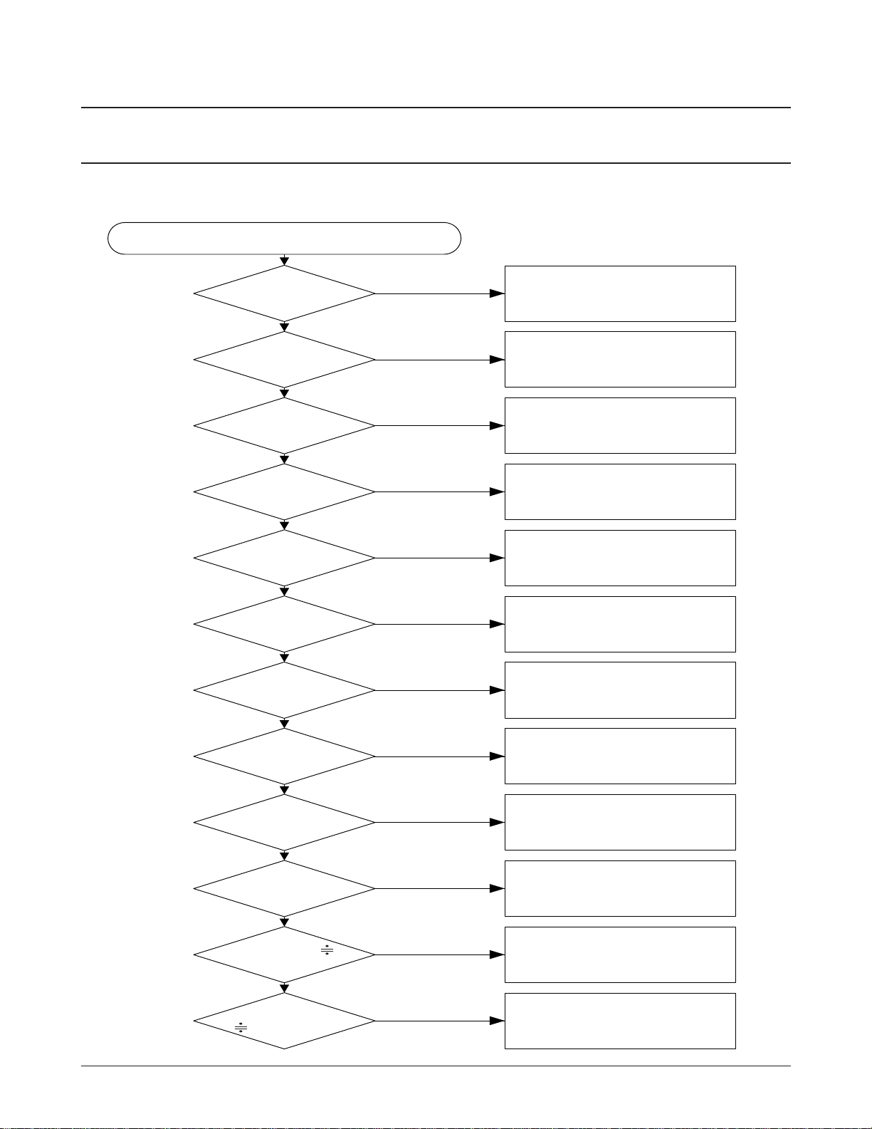
5. Troubleshooting
5-1 Main Set
5-1-1 RX Sensitivity Problem
Samsung Electronics 5-1
RX ON (RF Input - Frequency : CH Freq. + 20 kHz
- RF Amplitude : - 50 dBm)
U204 Input ≥ -60 dBm?
Yes
Yes
Yes
Yes
Yes
Yes
Yes
Yes
Yes
Yes
Yes
No
No
No
No
No
No
No
No
No
No
No
No
F200 Input ≥ -60 dBm?
Q200 pin 1 ≥ -65 dBm?
Q200 pin 3 ≥ -50 dBm?
F101 Input ≥ -50 dBm?
U102
Input (pin47, 48)
≥ -55 dBm?
U102 pin 42, 43
≥ -50 dBm?
F100
pin 4, 5 ≥ -50 dBm
(225 MHz)?
U102
pin 38, 39 ≥ -55 dBm
(225 MHz)?
U102 pin 36, 37
≥ -45 dBm (45MHz)?
U102
pin 25, 26, 27, 28 30
mVp_p(20KHz)?
U411 pin 7, 14
1Vp_p(20KHz)?
Check U204, J401, C223
Solder Status k Resolder
Check U109, U204, C224, F200
Solder Status k Resolder
Check C219, L205, C217, C218, C216,
R219 Solder Status k Resolder
Q200, C216 Resolder or Replace
Check L207, L206, R221, C220, C170,
F101 Solder Status k Resolder
Resolder C172, L104, C171
Check U102 (pin 42, 43, 44, 47, 48),
R107, R109, C925, U839, C926, R504
Resolder or Change
Check C168, C167, C164, R137,
F100, C169, L108, L106, R138
Solder status k Resolder
Check C160, C159, C161, C162,
L105, L204 k Resolder or Charge
Check U102, C164, L161
Solder status k Resolder
Resolder or Check U102, C124,
L101, C119, R112 k Resolder
U411, C464, C445, L403, R466, L404,
R465, R462, R468, R443, R445, R444,
L401, L402, R447 k Resolder
5-2 Samsung Electronics
Troubleshooting
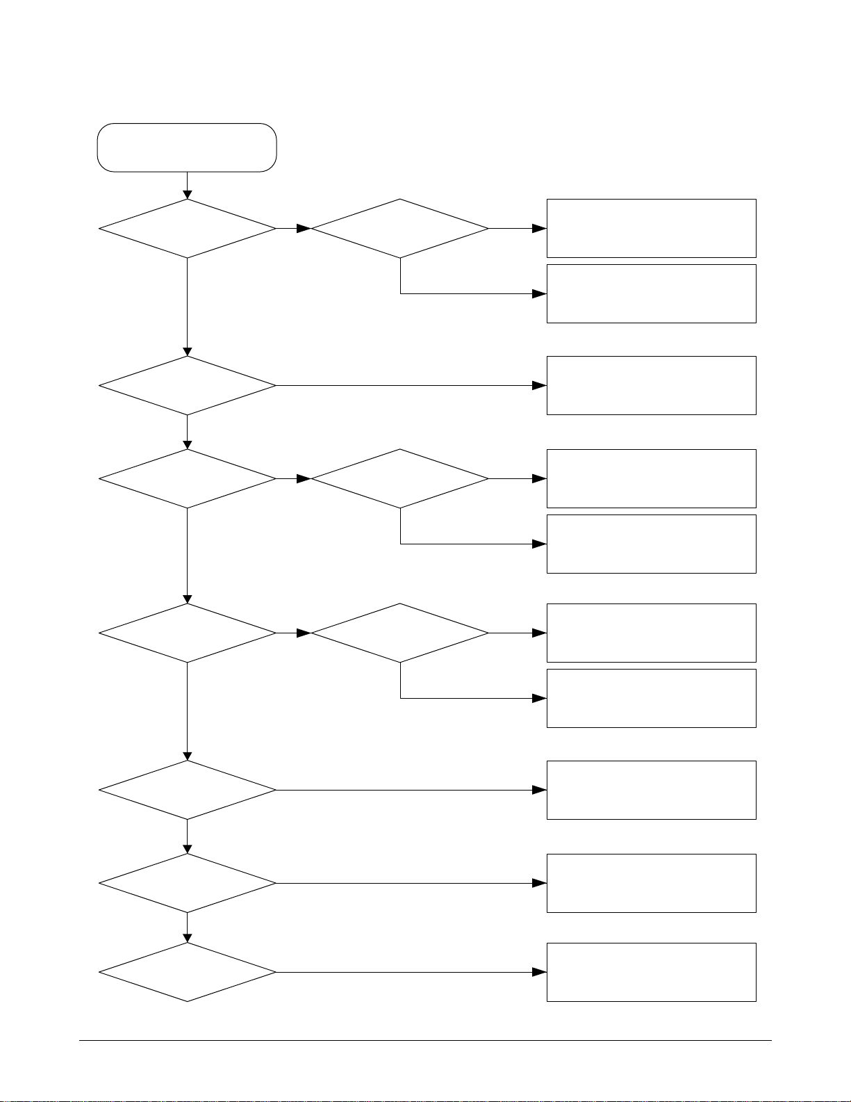
5-1-2 TX Power Problem
CH.60 (902 MHz) &
Tx Carrier ON (Power level 5)
F201 Input ≥ - 10 dBm?
RF VCO
≥ -10dBm(1172MHz)?
IF VCO ≥ -10dBm(540MHz)?
TX VCO ≥ -10dBm
(902MHz)?
U202 pin 4
≥ 2.0Vp_p(AC)?
U202, U204, U205, C225 Resolder
or change poor component(s)
R139, C174, U204, U109
Resolder or Change U204, U109
C223, U204 J410 pin 21 Resolder
F201 Resolder or Change F201
ResolderC208, U202 or
replace if damaged.
Resolder R215, C213, R212, C214,
R213, C210, U206, U205,
U202,U203 or replace if damaged.
Resolder FB100, U202, U204
or replace if damaged.
Resolder C147, C146, R135, R133,
R134, R132, R131, C142, C138, C139,
R504, C165, C927, R121, R120, R123,
C130 or replace if damaged.
Check R208,R209,R210, C943,
F201 or replace if damaged.
F201 Output ≥ -15 dBm?
U202 Input ≥ - 15 dBm?
U202 Output ≥ 30 dBm?
U204 Input ≥ 30 dBm?
U204 Output ≥ 30 dBm?
I/F Connector pin 21
≥ 30 dBm?
Yes
Yes
Yes
No
No
No
Yes
No
Yes Yes
No
Yes
No
Yes
No
No
No
U202 pin 5
voltage ≥ 3V rms?
Resolder U202 or
replace if damaged.
Yes
No
Samsung Electronics
5-3
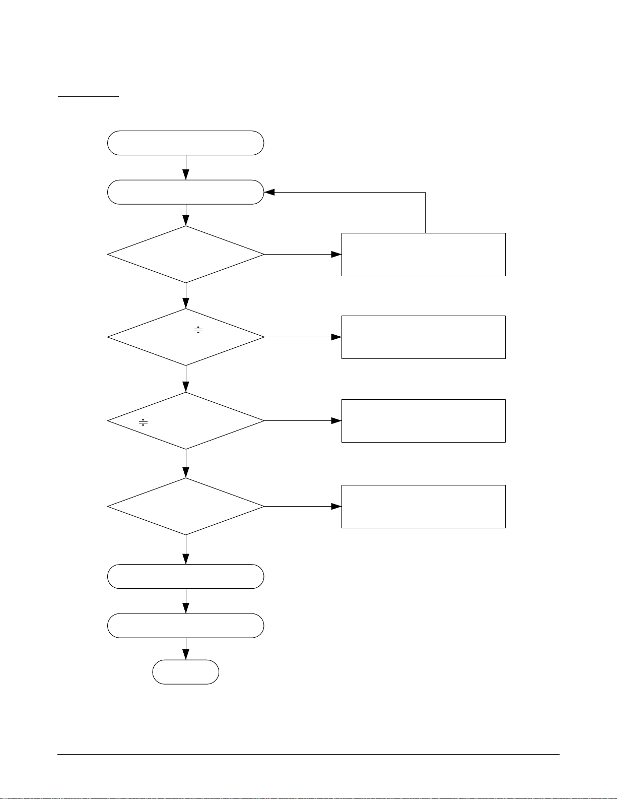
5-1-3 Base Band
POWER ON
Troubleshooting
‘POWER ON’ does not work
Give Battery Power
Check the Battery Voltage
is less than 3.2V
Charge the Battery
Check the path from BATT to U402
Check the path from D401 to U402
(DC/DC convert circuit)
Check the clock generation circuit
(related to U201 and U200)
U402 pin 5 3.6V
(when pushing pwr Key)
U402 pin 2, 3, 4
3.3V (when pusging
pwr Key)
Check for the clock siganl
at U408 pin 83
Check J301
Check the initial operation
END
Yes
No
No
Yes
No
Yes
No
Yes
 Loading...