

Page 1

© Samsung Electronics Co.,Ltd. Jan. 2000
Printed in Korea
AD68-00079L
SERVICE MANUAL
SDC-80
DIGITAL CAMERA
SDC-80
SERVICE
1. Introduction
2. Specifications
3. Disassembly and Reassembly
4. Exploded View and Parts List
5. Adjustment
6. Electrical Parts List
7. PCB Diagrams
8. Wiring Diagram
9. Schematic Diagrams
Manual
DIGITAL CAMERA
CONTENTS
Page 2

UPDATE LOG SHEET
Use this page to keep any special servicing information. (Service Bulletin, etc.)
If only parts number changes, Just change parts number directly on parts list.
And if you need more information, please see the service bulletin
Application Data Page Part # Note(Cause & Solution) S/Bulletin #
Page 3

Samsung Electronics 1-1
The program is to adjust a camera and diagnose a fault when the unit is serviced. The program isn't provided for customers and only service center to check the camera setting without disassembling and read/modify the camera control value. Some functions not required in service center aren't used.
1. Provision for program
The program isn't provided with the additional disc and must be downloaded from Single.
2. System Requirements
1. IBM compatible PC (pentium standard)
2. Windows 95 & Mouse
3. Video Card supported more than 256 color
4. 5MB Hard disk space
3. Program Functions
1. SSFDC(SMART MEDIA) FORMAT, DELETE ALL
2. FUNCTION KEY TEST
3. LCD PIXEL TEST
4. LOGO TEST
5. CONTROL LED TEST, LCD PANEL TEST
6. MACRO MODE CHECK, VIDEO JACK TEST, STROBO (FLASH) JACK CHECK
7. OSD (ON SCREEN DISPLAY) OFF
8. PC SHOT, SELF TIMER SHOT
9. AE ADJUSTMENT
10. 3100K, 5100K WHITE BALANCE ADJUSTMENT
11. JPEG, THUMBNAIL DOWN LOAD
12. BACK FOCUS ADJUSTMENT MODE
13. POWER CONSTANT ON
14. RS-232C CHANGER TEST
15. NTST, PAL CONVERT ADJUSTMENT
4.Installing Program
1. Unzip the Dscstudi.zip file downloaded from Single in a folder.
2. Execute the Setup.exe file in the unzipped files.
3. Install as dialog box's message.
4. After completing the installation, check to run the DSCStudio.exe file in the folder where program is
installed.
* Generally, it is created in C:\Program files\Samsung\DSCStudio.
1. Introduction
1-1. Camera Adjustment Program
1-1-1. About the Program
Page 4
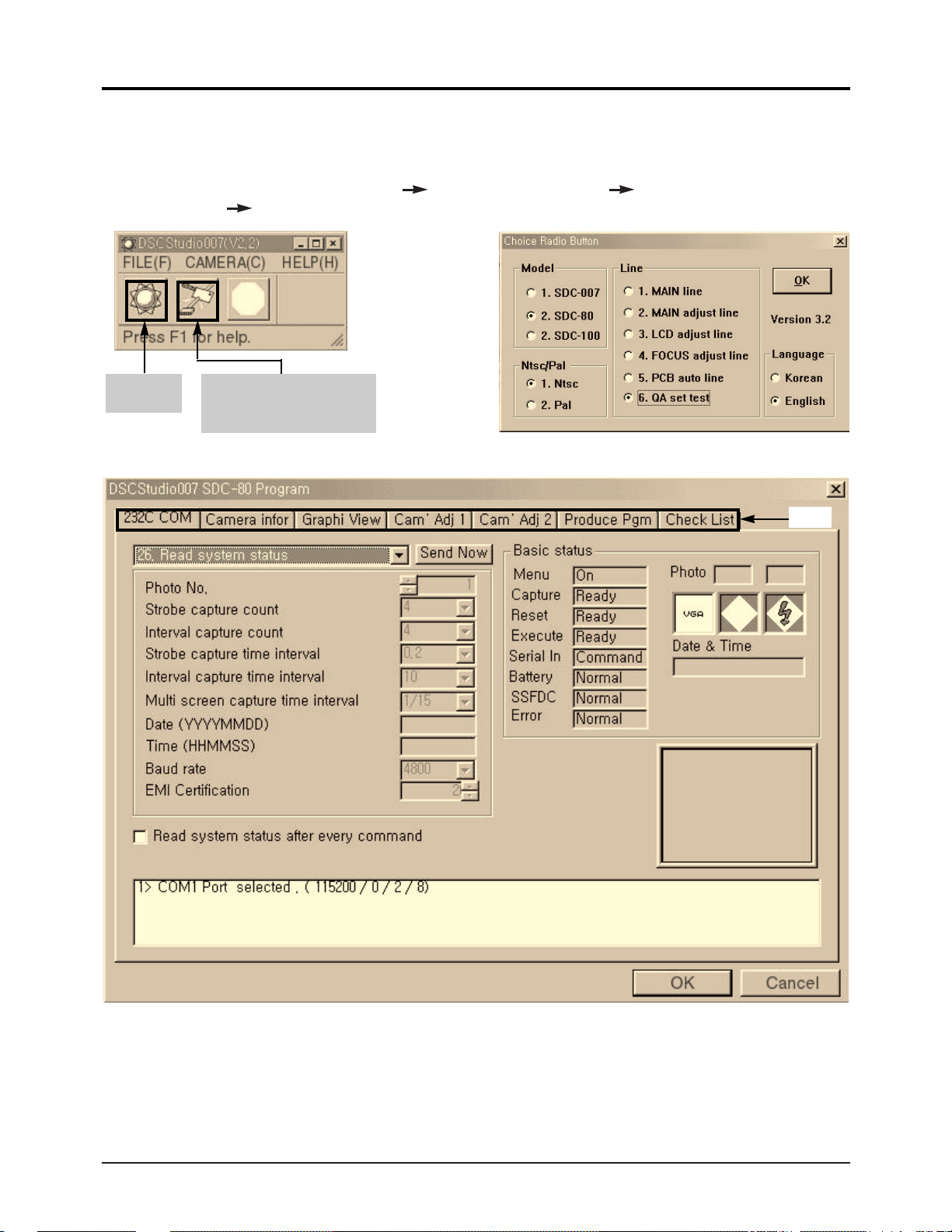
(Figure 3) Basic communication dialog box
(Figure 1) Initial screen dialog box
(Figure 2) Choice screen dialog box
• Program start : Turn on PC for Windows Connect PC with camera Power on camera
Execute DSCStudio.exe in Windows
About TAP : • Camera Adjustment I : (see Figure 5) •Camera Adjustment II : (see Figure 6)
• View Graphic File : (see Figure 7) •Test Options : (see Figure 8)
• PGM for Manufacturing : (see Figure 9)
Samsung Electronics1-2
Introduction
1-1-2. DSCStudio Description
Start DSC
studio.
Set up Communication
port and communication
speed.(see Figure 4)
TAP
Page 5
• Describe the relevant things only in (Figure 4).
1. In the DCAM_PARAMETER, the DTL_Glain value is used for HeXa value.
For instance, if DTL_Gain=2631720 is translated into HeXa, it means 0x282828. So y=0x28, Cr=0x28 and
Cb=0x28.
2. In the LCD_Control, the settings are EVR value and also affect LCD output.
3. The Color Bar ON/OFF option can be used to display color bar with LCD and VIDEO OUT.
4. The Update option can be used to write the currently displayed number with EEPROM.
5. The Restore option can be used to restore to the first loaded value (EEPROM value before updating).
6. The Format option can be used to write the EEPROM default value saved in dscdtuio007.ini. of the
window folder.
("0xff" is the initially empty EEPROM value.)
Note) The Format is similar to the Format with LCD option without LCD control value.
7. The Reload option can be used to display the currently recorded EEPROM value on the screen.
*Note
- The model set value is 007 in the PGM mode. However, error occurred when 80 sets are connected to
adjust.
- Make sure that the testing model is the same with the running model in program.
Samsung Electronics1-4
Introduction
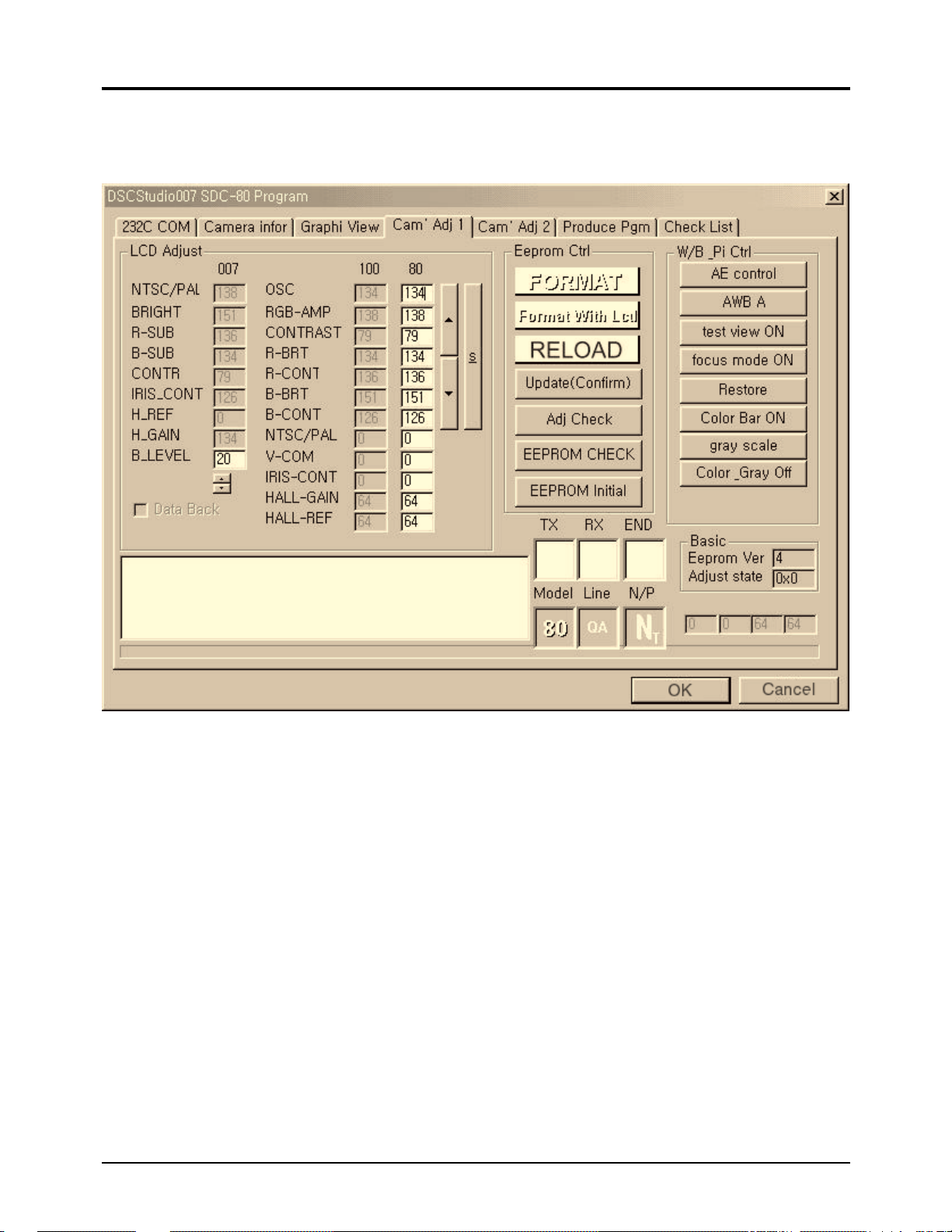
(Figure 5) Camera Adjustment I
Page 6
Samsung Electronics1-6
Introduction
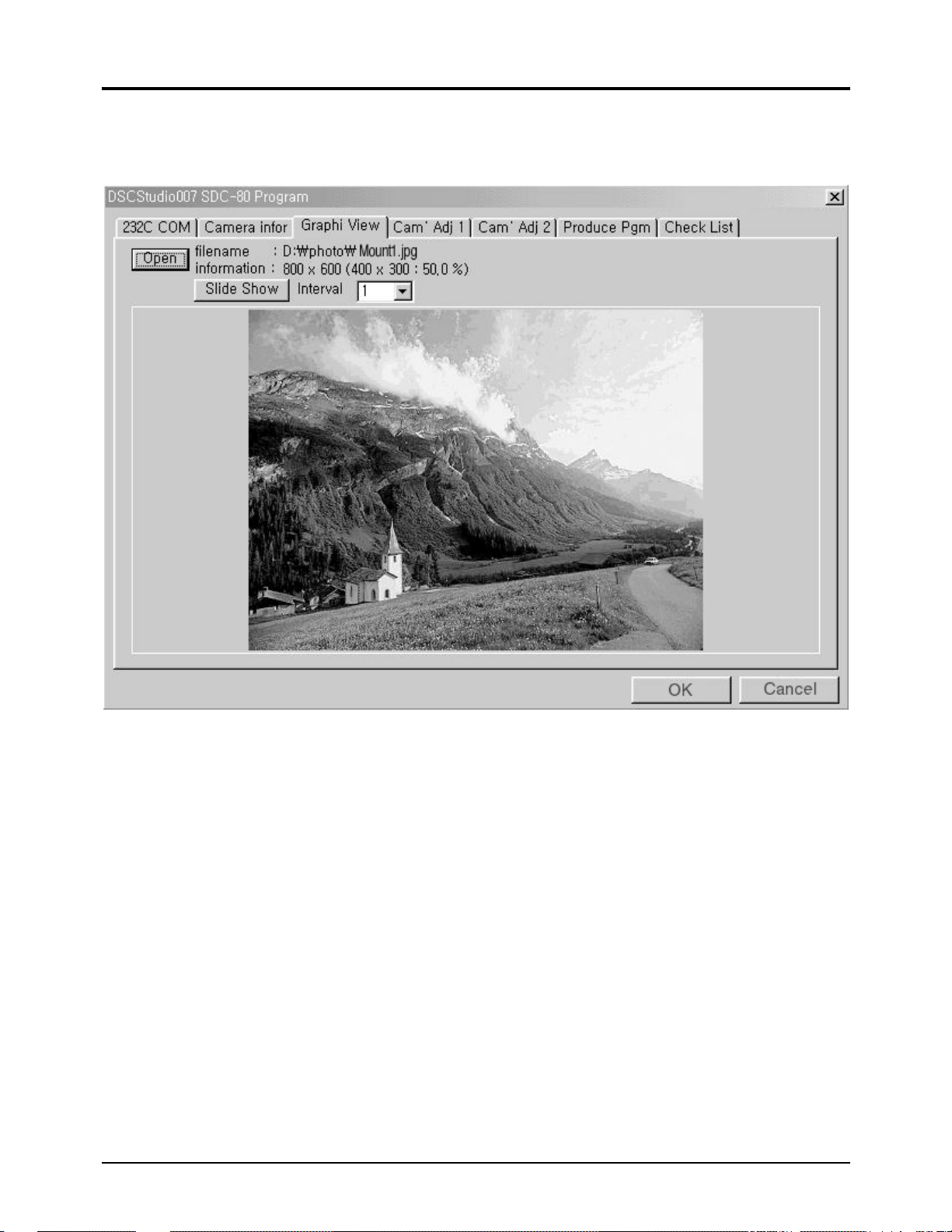
• The JPEG image can be displayed without any image edit program.
1. Click the Open button to display the file saved as a JPEG format.
2. Click the Slid Show button to display the file containing in the option at an specified interval.
(Figure 7) View Graphic File
Page 7
Samsung Electronics1-8
Introduction
11.Black Level Adj:
12.AE Adjustment: Adjust the Hall value automatically.
13.3100K W/B test : Set 3100K(incandescent light temperature) white balance.
14.5100K W/B test : Set 5100K(fluorescent light temperature) white balance.
15.Thumbnail Down load : Transfer thumbnail image in the smart media card into PC.
16.JPEG Down Load : Transfer image in the smart media card into PC.
17.Shot 0: Function SHUTTER in camera photo mode.
18.Shot 0: Function SHUTTER in camera photo mode.
19.Shot 0: Function SHUTTER in camera photo mode.
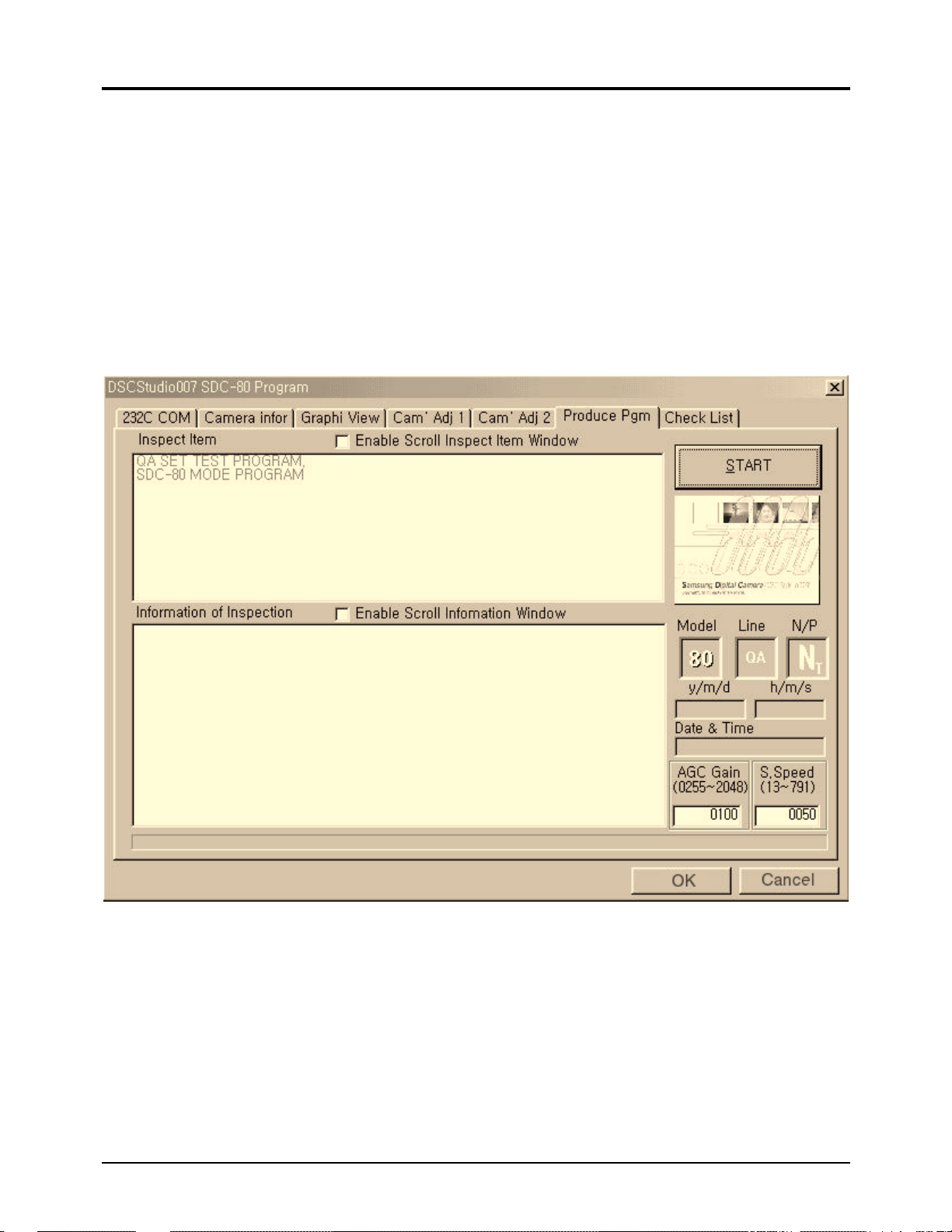
• Run the PI program.
The settings of the Test Options (see Figure 7) are applied as a sequence.
Click the START button to run.
The edit function is enabled when Vs appear in the check boxes of Enable Scroll Inspect Item Window
and Enable Scroll Information Window.
(Figure 9) PGM for Manufacturing
Page 8
Samsung Electronics 2-1
2. Specifications
✤ The technical specifications and design may be changed without notice.
System Specifications
CCD
Progressive 0.85M pixel
Number of pixels 1024 x 768 pixel (XGA)
Color Depth 24 bits True Color
Memory capacity Extra (smart media card 4MB/3.3V)
Image Capacity Standard (quality-about 20/high quality-about 10)
Lens Dual fixed focus F:2.8f = 6.6
Focus Length Normal (50cm ~ ) Macro (5 ~ 50cm)
View Finder OVF (optical view finder) & color LCD
Shutter Speed Electric Shutter (1/8 ~ 1/2000)
Exposure Auto / Manual
White Balance Auto
Video Out Both NTSC type & PAL type
Power Source 5.0V:Atype battery, 3.6V:Li-ion charger
PC Interface Serial Transmission (RS 232C : Max 115.2kbps)
Compression Standard JPEG
Support O/S MS-Windows 95, 98
S/W CD-Rom (TWAIN Driver, iPhotoExpress)
Dimensions 102 x 75 x 40 (Length x Height x Width)
Net Weigh
Less than 199g (not including battery pack)
Basic Shooting
Mode
Full Size Shooting : 1152 x 864 (SQ/HQ)
General Shooting
Standard Shooting
VGA Size Shooting : 640 x 480 (SQ/HQ)
B/W Shooting Full Size B/W : 1152 x 854 (SQ/HQ)
Special Shooting
Mode
Multi Shooting
Full Size Division : 1152x 864 (SQ/HQ)
- 4 ~ 16 Images Division
Continuous
Shooting
VGA Size continuation : 640 x 480 (SQ/HQ)
- 3 ~ 6 Images Division
Play Mode
Normal Playback One Image at a time, full size playback
Magnified Playback 4 times magnified playback by parts
Multi Playback 6 images-divided multi playback
Automatic Playback Automatic interval playback
Erase Mode
Selective Erase Erase selected images among divided images
Full Erase Erase all the memories
Erase Prevention Prevent accidental erase of precious images
Setting Mode Menu bar type control for each status
Transmission Mode PC interfacing only mode
Others
- Direct interfacing mode
- Manual adjust mode : adjusting exposure
- Navigation key control : 4-direction movement and selection
Page 9

Samsung Electronics2-2
Specifications
MEMO
MEMO
Page 10
Samsung Electronics 3-1
3. Disassembly and Reassembly
3-1. Cabinet Disassembly
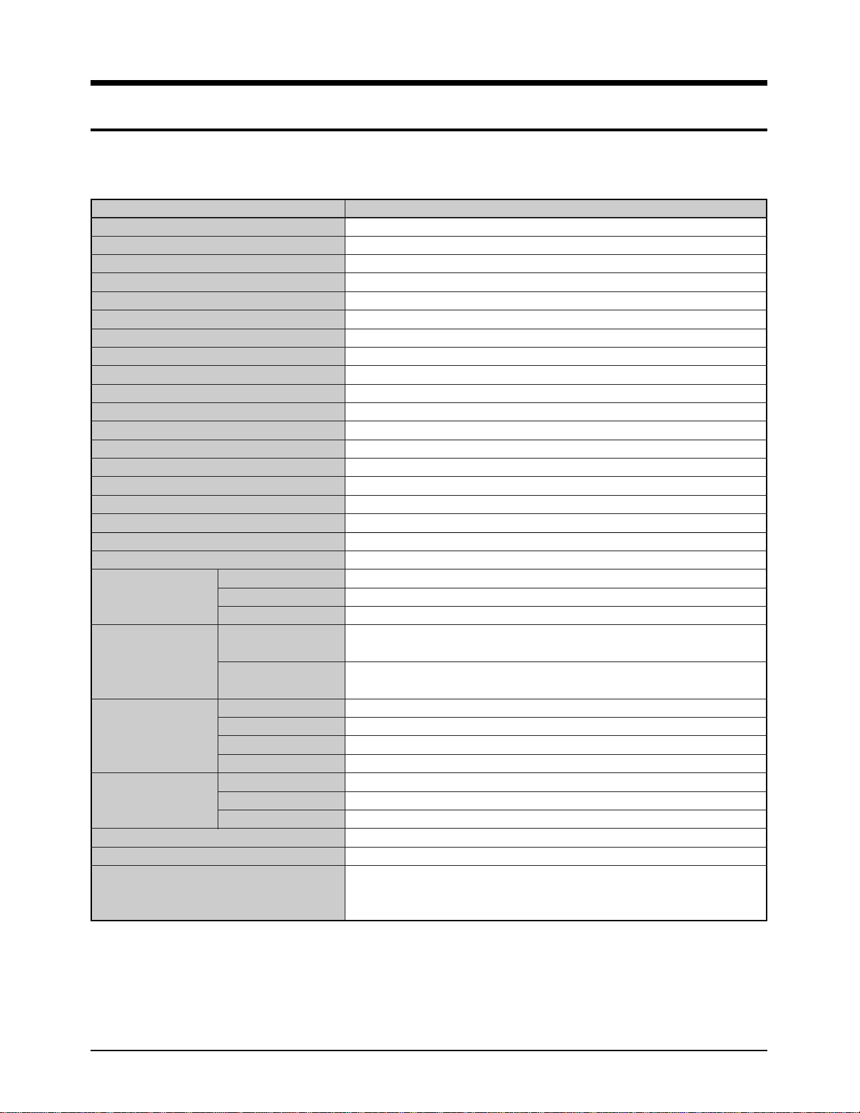
3-1-1. Ass’y CASE-TOP Removal
Fig. 3-1 Ass’y CASE-TOP Removal
Remove the INLAY.
Remove 2 screws.
Remove the CASE-TOP.
Remove 1 screw.
Remove the INLAY.
Page 11
Samsung Electronics3-2
Disassemblr and Reassembly
3-1-2. Ass’y CASE-BOTTOM Removal
Fig. 3-2 Ass’y CASE-BOTTOM Removal
Remove the CASE-BOTTOM.
Remove 3 screws.
Remove 1 screw.
Page 12
Samsung Electronics3-4
Disassemblr and Reassembly
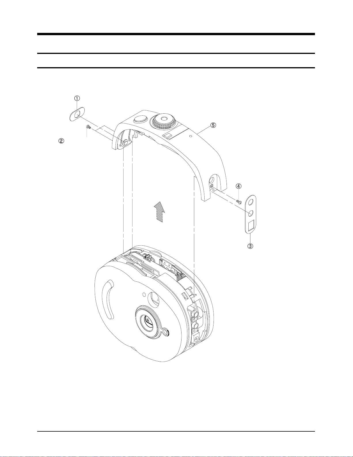
3-1-4. Ass’y CASE-FRONT Removal
Fig. 3-4 Ass’y CASE-FRONT Removal
Remove 2 screws.
Remove the CASE-FRONT.
* Be careful to assemble MACRO-LEVER with LENS-MACRO when assembling the case-front.
Page 13
Samsung Electronics3-6
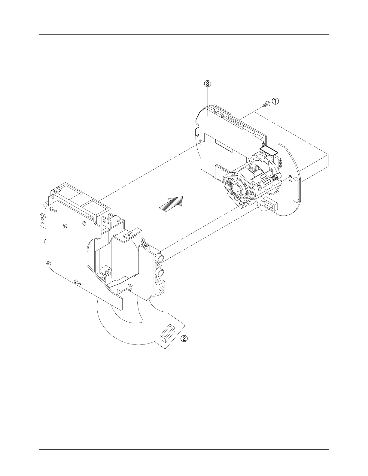
Disassemblr and Reassembly
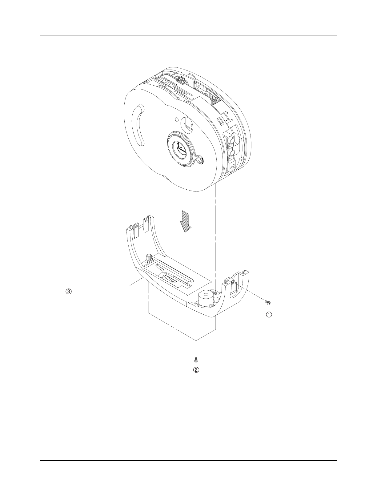
Fig. 3-6 Ass’y MAIN Removal
3-1-6. Ass’y MAIN Removal
Remove the ASSY-MAIN.
Remove the
3screws.
Remove the FPC-MAIN from MAIN-PCB.
Page 14
Samsung Electronics3-8
Disassemblr and Reassembly
¡¨BATT + ¡¨
¡¨BATT - ¡¨
Fig. 3-9 Connector Diagrams
3-3. Connector Diagrams
1
4
10
12
14
16
6
6
6
DIRECTION
MAIN BOARD DC-BOARD
MAIN BOARD JACK BOARD
MAIN BOARD ASSY-LENS
MAIN BOARD REAR BOARD
MAIN BOARD FUNT-BOARD
MAIN BOARD TFT-LCD
FUNT-BOARD ASSY-STROBO
DC-BOARD JACK-BOARD
DC-BOARD BATTERY +, -
REAR-BOARD LCD-B/L
NO. NO.
CONNECTOR
CN02
CN02
CN03
CN05
CN04
CNL01
CNF03
CNP02
CNP02
CNB02
CONNECTOR
CNP03
CNJ02
LENS-FPC
CNB01
CNF01
LCD-FPC
STROBO
CNJ03
BATTERY
HBL
1
2
3
5
11
13
15
18
9
7
8
Page 15

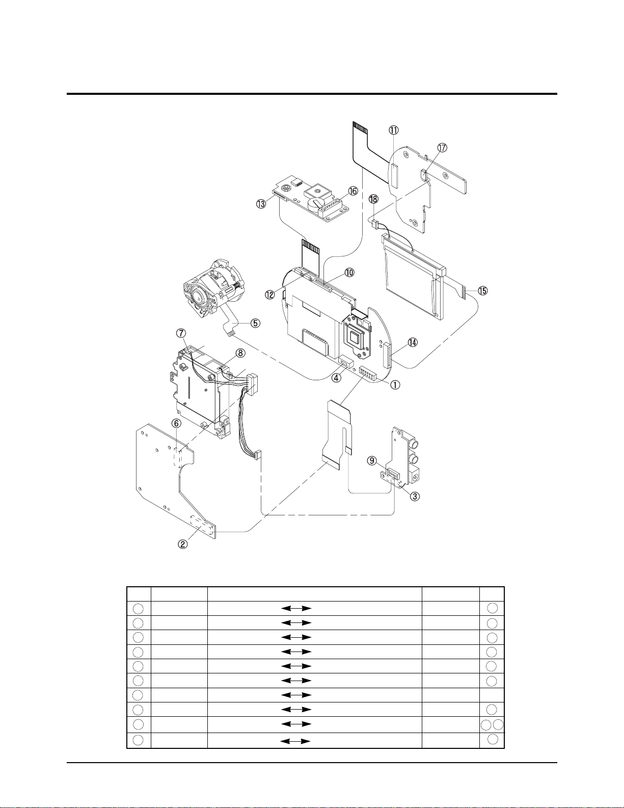
Samsung Electronics 4-1
4-1. Cabinet Assembly 4-2
4-2. Parts List 4-3
4. Exploded View and Parts List
Page 16

Samsung Electronics4-2
Exploded View and Parts List
4-1 Cabinet Assembly
101
102
100
105
700
106
105
104
103
400
702
402
403
401
703
701
300
302
308
307
306
305
304
303
310
309
702
703
702
702
301
500
702
800
507
702
504
701
701
700
502
503
506
505
701
702
702
501
508
600
601
608
701
610
702
606
705
607
603
602
605
604
609
200
208
207
105
202
203
701
204
702
701
201
205
206
105
Page 17

Loc. No New Part No Description and Specification Remark Remark
505 AD64-00139A DOOR-LOCK;-,POM WHT,-,-,-,-,-,SDC-X80
506 AD61-00176A SPRING-DOOR BATT;-,SUS T=0.3,-,-,-,-,-,507 AD61-00174A HOLDER-BATT,R;-,ABS,-,-,-,SDC-X80
508 AD97-01067A ASSY-DC/DC BOARD;SDC-80,-,ASSY -DC/DC B
600 AD97-01065A ASSY-MAIN BOARD;SDC-80,-,ASSY -MAIN BOA
601 AD66-30597A LEVER-MACRO;-,ABS,HB,-,-,SDC-007
602 AD29-00003A FILTER-OLP;-,OG-BF458,O.L.P.F,-,-,TR
603 AD73-00016A RUBBER-CCD;SILICON,-,SDC-X80,604 AD61-00175A PLATE-CCD;-,AL PLATE T=0.8,-,-,SDC-X80
605 AD99-40009U ASSY-MAIN BOARD,c;SDC-X80,-,ASSY -MAIN B
606 AD63-00122A SHIELD-SUB;-,PBS T0.15,-,-,SDC-80
607 AD97-01702A ASSY-SHIELD CASE MAIN;SDC-80,-,608 AD97-00315A ASSY—DSC-LENS;SDC-007,ASSY,PANFOCUS
609 AD97-01472A ASSY-FPC MAIN;SDC-80,FPC MAIN,40*26*T0.6
610 AD41-00097A FFC—FUNC,22PIN;FLATCABLE,0.3,22,SDC-80
700 6002-001094 SCREW-TAPPING;CH(0.5),+,B,M1.7,L3.5,NI P
701 AC60-12128B SCREW-TAPTITE;-,BH,-,TAP,1.7,4,702 AD60-00014A SCREW-MACHINE;-,-,-,-,-,-,-,-,WHT
703 6001-001288 SCREW-MACHINE;CH(0.5),+,M1.7,L6.0,NI PLT
704 AC60-10024A SCREW-MACHINE;BH,+,M2,X3,FZW,FE,-,-,705 AH60-10112A SCREW-TAPTITE;PH,+,M2,L5,SN1,-,YEL
800 AD97-01491A ASSY-OVF-LENS;SDC-80,ASSY,-
Exploded View and Parts List
4-4
Page 18

Samsung Electronics 5-1
5. Adjustment
5-1. Camera Adjustment
5-1-1. Focus Adjustment
• Adjusting in the Photo Mode
1. Connect the camera and TV to video output cable. Turn on the power and set to the PC mode.
2. Aim the Main board at the focus chart placed 2.5 meters away and perpendicular to the center of the
lens.
3. Loose a fixing screw lightly positioned in front of a lever in the state of pulling back macro lever
toward °ƒ (counterclockwise at the front).
4. Turn the focus adjusting lever until a lever is in focus through the TV screen (not to move the macro
lever).
5. Tighten the fixing screw when the lever is in focus.
* In the Photo mode, the state of the focus may be difficult to check. If it isn’t, you can adjust in Resume
mode or with program for adjustment after taking a photograph.
• Adjusting with Program for Adjustment
* If the program for adjustment is used, the 3 times magnified screen allows you exactly to adjust camera.
1. Connect the camera to TV and PC with video output cable and PC connecting cable. Turn on the power
and set to the PC mode.
2. Aim the Main board at the focus chart placed 2.5 meters away and perpendicular to the center of the
lens.
3. After running the program for adjustment on the PC to click the Focus Mode On button in the Camera
Adjustment mode.
4. Repeat step 3 through 5 of “Adjusting in the Photo Mode”.
5. Click the Focus Mode On button and finish the program for adjustment.
(Focus Adjustment)
Focus Adjusting Lever
Fixing screw
(Lens & Lever Position)
2.5 m
LENS
FOCUS CHART
MAIN BOARD
Page 19

Samsung Electronics5-2
Adjustment
5-1-3. Program for Adjustment
5-1-2. MCLK Adjustment
1. Turn on camera power and set to Photo mode.
2. One adjustment point is TP1-MCLK. Adjust using CT301.
3. Connect probe of frequency counter with TP1.
4. Using CT301, adjust it so that MCLK is 54.00MHz+00Hz.
(External view of PCB :Main Board component side)
Page 20

Samsung Electronics5-4
Adjustment
5-2-3. Adjustment
1. PD
1) TPL6-OSC & OSC mode
2) - Connect the probe of oscilloscope to TPL-OSC.
- Press the UP/DOWN button or the number buttons so that the A is
2.0µs ± 0.2µs (when NTSC).
3) Using the UPDATE button, store the adjusted value in the EEPROM.
* Using OSC or CSHD, adjust the trigger.
2. BRIGHTNESS
1) TPL2-VG & RGB-AMP mode
2) - Connect the probe of oscilloscope to TPL2-VG.
- Press the UP/DOWN button or the number buttons so that the B
level (between blacks) is 3.5 ± 0.1Vp-p.
3) Using the UPDATE button, store the adjusted value in the EEPROM.
* Using FRP(or use No. 2 - 7 alignment wave form in common), adjust
the trigger.
3. CONTRAST
1) TPL2-VG & CONTRAST mode
2) - Connect probe of oscilloscope to TPL2-VG.
- Press the UP/DOWN button or the number buttons so that the C
level (between black and white) is 3.0 ± 0.1Vp-p.
3) Using the UPDATE button, store the adjusted value in the EEPROM.
4. R-BRIGHT
1) TP3-VR & R-BRT mode (Bright wave form)
2) - Connect the probe of oscilloscope to TP3-VR.
- Press the UP/DOWN button or the number buttons so that the B
level (between pedestals) is 3.5 ± 0.1Vp-p.
3) Using the UPDATE button, store the adjusted value in the EEPROM.
5. R-CONTRAST
1) TPL3-VR & R-CONT mode (Contrast wave form)
2) - Connect the probe of oscilloscope to TPL3-VR.
- Press the UP/DOWN button or the number buttons so that the C
level is 3.0 ± 0.1Vp-p.
3) Using the UPDATE button, store the adjusted value in the EEPROM.
6. B-BRIGHT
1) TPL1-VB & B-BRT mode (Bright wave form)
2) - Connect the probe of oscilloscope to TPL1-VB.
- Press the UP/DOWN button or the number buttons so that the B
level is 3.5 ± 0.1Vp-p.
3) Using the UPDATE button, store the adjusted value in the EEPROM.
PD wave form
BRIGHT wave form
CONTRAST wave form
Page 21

Samsung Electronics5-6
Adjustment
MEMO
MEMO
Page 22

Samsung Electronics 6-1
Electrical Parts List
6. Electrical Parts List
Loc. No Part No Desc & Spec Remark
AD97-01065A ASSY-MAIN BOARD
B03 3301-001051 CORE-FERRITE BEAD;AC,1.6X0.8X0.8mm,-,B04 3301-001051 CORE-FERRITE BEAD;AC,1.6X0.8X0.8mm,-,B05 3301-001051 CORE-FERRITE BEAD;AC,1.6X0.8X0.8mm,-,B06 3301-001051 CORE-FERRITE BEAD;AC,1.6X0.8X0.8mm,-,-
B07 3301-001051 CORE-FERRITE BEAD;AC,1.6X0.8X0.8mm,-,B08 3301-001051 CORE-FERRITE BEAD;AC,1.6X0.8X0.8mm,-,B09 3301-001051 CORE-FERRITE BEAD;AC,1.6X0.8X0.8mm,-,B10 3301-001051 CORE-FERRITE BEAD;AC,1.6X0.8X0.8mm,-,B11 3301-001051 CORE-FERRITE BEAD;AC,1.6X0.8X0.8mm,-,-
B12 3301-001051 CORE-FERRITE BEAD;AC,1.6X0.8X0.8mm,-,B13 3301-001051 CORE-FERRITE BEAD;AC,1.6X0.8X0.8mm,-,B14 3301-001051 CORE-FERRITE BEAD;AC,1.6X0.8X0.8mm,-,B15 3301-001051 CORE-FERRITE BEAD;AC,1.6X0.8X0.8mm,-,B17 3301-001051 CORE-FERRITE BEAD;AC,1.6X0.8X0.8mm,-,-
B19 3301-001051 CORE-FERRITE BEAD;AC,1.6X0.8X0.8mm,-,- REV.03change
B20 3301-001051 CORE-FERRITE BEAD;AC,1.6X0.8X0.8mm,-,B21 3301-001051 CORE-FERRITE BEAD;AC,1.6X0.8X0.8mm,-,B23 3301-001051 CORE-FERRITE BEAD;AC,1.6X0.8X0.8mm,-,B25 3301-001051 CORE-FERRITE BEAD;AC,1.6X0.8X0.8mm,-,-
BD41 3301-001051 CORE-FERRITE BEAD;AC,1.6X0.8X0.8mm,-,BD42 3301-001051 CORE-FERRITE BEAD;AC,1.6X0.8X0.8mm,-,BD61 3301-001051 CORE-FERRITE BEAD;AC,1.6X0.8X0.8mm,-,C01 2203-000189 C-CERAMIC,CHIP;100nF,+80-20%,25V,Y5V ,TP,
C02 2203-000189 C-CERAMIC,CHIP;100nF,+80-20%,25V,Y5V ,TP,
C03 2203-000189 C-CERAMIC,CHIP;100nF,+80-20%,25V,Y5V ,TP,
C04 2203-000681 C-CERAMIC,CHIP;0.027nF,5%,50V,NP0,TP,160
C05 2203-000626 C-CERAMIC,CHIP;0.022nF,5%,50V,NP0,TP,160
C051 2203-000681 C-CERAMIC,CHIP;0.027nF ,5%,50V,NP0,TP,160
C06 2203-000189 C-CERAMIC,CHIP;100nF,+80-20%,25V,Y5V ,TP,
C07 2203-000189 C-CERAMIC,CHIP;100nF,+80-20%,25V,Y5V ,TP,
C08 2203-000189 C-CERAMIC,CHIP;100nF,+80-20%,25V,Y5V ,TP,
C09 2404-000304 C-TA,CHIP;22uF ,20%,6.3V,-,TP,3528,C10 2203-000189 C-CERAMIC,CHIP;100nF,+80-20%,25V,Y5V ,TP,
C12 2203-000189 C-CERAMIC,CHIP;100nF,+80-20%,25V,Y5V ,TP,
Loc. No Part No Desc & Spec Remark
C15 2203-000998 C-CERAMIC,CHIP;0.047nF,5%,50V,NP0,TP,160
C16 2203-000626 C-CERAMIC,CHIP;0.022nF,5%,50V,NP0,TP,160
C17 2203-000189 C-CERAMIC,CHIP;100nF,+80-20%,25V ,Y5V,TP,
C18 2404-000151 C-TA,CHIP;1uF ,20%,16V,-,TP,3216,C19 2203-000189 C-CERAMIC,CHIP;100nF,+80-20%,25V ,Y5V,TP,
C211 2203-000041 C-CERAMIC,CHIP;0.01nF ,0.25pF,50V,NP0,TP,
C3 2203-000189 C-CERAMIC,CHIP;100nF,+80-20%,25V,Y5V,TP,
C31 2203-000189 C-CERAMIC,CHIP;100nF,+80-20%,25V ,Y5V,TP,
C32 2404-001020 C-TA,CHIP;10uF ,20%,10V,GP,TP,3216,3.2
C33 2203-000189 C-CERAMIC,CHIP;100nF,+80-20%,25V ,Y5V,TP,
C34 2203-000440 C-CERAMIC,CHIP;1nF,10%,50V,X7R,TP,1608,C41 2203-002793 C-CERAMIC,CHIP;1000nF,+80-20%,25V ,Y5V,TP
C42 2203-002793 C-CERAMIC,CHIP;1000nF,+80-20%,25V ,Y5V,TP
C43 2203-002793 C-CERAMIC,CHIP;1000nF,+80-20%,25V ,Y5V,TP
C44 2203-002793 C-CERAMIC,CHIP;1000nF,+80-20%,25V ,Y5V,TP
C47 2203-000189 C-CERAMIC,CHIP;100nF,+80-20%,25V ,Y5V,TP,
C48 2203-000189 C-CERAMIC,CHIP;100nF,+80-20%,25V ,Y5V,TP,
C51 2203-000257 C-CERAMIC,CHIP;10nF,10%,50V,X7R,TP,1608
C52 2404-001020 C-TA,CHIP;10uF ,20%,10V,GP,TP,3216,3.2
C53 2203-000189 C-CERAMIC,CHIP;100nF,+80-20%,25V ,Y5V,TP,
C54 2203-000189 C-CERAMIC,CHIP;100nF,+80-20%,25V ,Y5V,TP,
C60 2203-000189 C-CERAMIC,CHIP;100nF,+80-20%,25V ,Y5V,TP,
C61 2203-001598 C-CERAMIC,CHIP;2200nF,+80-20%,16V ,Y5V,TP
C64 2404-000304 C-TA,CHIP;22uF ,20%,6.3V,-,TP,3528,C65 2404-000304 C-TA,CHIP;22uF ,20%,6.3V,-,TP,3528,-
C66 2404-000304 C-TA,CHIP;22uF ,20%,6.3V,-,TP,3528,C67 2203-000189 C-CERAMIC,CHIP;100nF,+80-20%,25V ,Y5V,TP,
C68 2404-001020 C-TA,CHIP;10uF ,20%,10V,GP,TP,3216,3.2
C69 2203-000189 C-CERAMIC,CHIP;100nF,+80-20%,25V ,Y5V,TP,
C71 2203-000357 C-CERAMIC,CHIP;0.15nF,5%,50V,NP0,TP,1608
C72 2203-000257 C-CERAMIC,CHIP;10nF,10%,50V,X7R,TP,1608
C73 2203-000257 C-CERAMIC,CHIP;10nF,10%,50V,X7R,TP,1608
C74 2203-000560 C-CERAMIC,CHIP;220nF,+80-20%,25V ,Y5V,TP,
C75 2203-001634 C-CERAMIC,CHIP;33nF,10%,50V,X7R,TP,1608,
C81 2203-000257 C-CERAMIC,CHIP;10nF,10%,50V,X7R,TP,1608
Page 23

Samsung Electronics6-2
Electrical Parts List
Loc. No Part No Desc & Spec Remark
C82 2203-000257 C-CERAMIC,CHIP;10nF,10%,50V,X7R,TP,1608
C83 2404-001020 C-TA,CHIP;10uF ,20%,10V,GP,TP,3216,3.2
C84 2203-000257 C-CERAMIC,CHIP;10nF,10%,50V,X7R,TP,1608
C98 2203-000560 C-CERAMIC,CHIP;220nF,+80-20%,25V ,Y5V,TP,
CD01 2203-000189 C-CERAMIC,CHIP;100nF,+80-20%,25V,Y5V ,TP,
CD02 2404-001020 C-TA,CHIP;10uF,20%,10V ,GP,TP ,3216,3.2
CD04 2404-001020 C-TA,CHIP;10uF,20%,10V ,GP,TP ,3216,3.2
CD05 2203-000189 C-CERAMIC,CHIP;100nF,+80-20%,25V,Y5V ,TP,
CD06 2203-000189 C-CERAMIC,CHIP;100nF,+80-20%,25V,Y5V ,TP,
CD07 2203-000189 C-CERAMIC,CHIP;100nF,+80-20%,25V,Y5V ,TP,
CD08 2203-000440 C-CERAMIC,CHIP;1nF,10%,50V,X7R,TP,1608,CD09 2203-000440 C-CERAMIC,CHIP;1nF,10%,50V,X7R,TP,1608,CD10 2203-000189 C-CERAMIC,CHIP;100nF,+80-20%,25V,Y5V ,TP,
CD11 2203-000189 C-CERAMIC,CHIP;100nF,+80-20%,25V,Y5V ,TP,
CD12 2203-000189 C-CERAMIC,CHIP;100nF,+80-20%,25V,Y5V ,TP,
CD13 2203-000189 C-CERAMIC,CHIP;100nF,+80-20%,25V,Y5V ,TP,
CD14 2203-000189 C-CERAMIC,CHIP;100nF,+80-20%,25V,Y5V ,TP,
CD15 2203-000189 C-CERAMIC,CHIP;100nF,+80-20%,25V,Y5V ,TP,
CD16 2203-000189 C-CERAMIC,CHIP;100nF,+80-20%,25V,Y5V ,TP,
CD17 2203-000189 C-CERAMIC,CHIP;100nF,+80-20%,25V,Y5V ,TP,
CD18 2203-000189 C-CERAMIC,CHIP;100nF,+80-20%,25V,Y5V ,TP,
CD21 2203-000041 C-CERAMIC,CHIP;0.01nF,0.25pF,50V,NP0,TP,
CD22 2203-000041 C-CERAMIC,CHIP;0.01nF,0.25pF,50V,NP0,TP,
CD23 2203-000041 C-CERAMIC,CHIP;0.01nF,0.25pF,50V,NP0,TP,
CD24 2203-000257 C-CERAMIC,CHIP;10nF,10%,50V,X7R,TP,1608
CD25 2203-000189 C-CERAMIC,CHIP;100nF,+80-20%,25V,Y5V ,TP,
CD26 2203-000189 C-CERAMIC,CHIP;100nF,+80-20%,25V,Y5V ,TP,
CD27 2404-001020 C-TA,CHIP;10uF,20%,10V ,GP,TP ,3216,3.2
CD28 2203-000189 C-CERAMIC,CHIP;100nF,+80-20%,25V,Y5V ,TP,
CD31 2203-000189 C-CERAMIC,CHIP;100nF,+80-20%,25V,Y5V ,TP,
CD32 2404-000212 C-TA,CHIP;3.3uF,20%,25V ,-,TP,3528,CD33 2203-000189 C-CERAMIC,CHIP;100nF,+80-20%,25V,Y5V ,TP,
CD34 2404-000238 C-TA,CHIP;4.7uF,20%,20V ,-,TP,3528,CD35 2203-000189 C-CERAMIC,CHIP;100nF,+80-20%,25V,Y5V ,TP,
CD36 2203-000189 C-CERAMIC,CHIP;100nF,+80-20%,25V,Y5V ,TP,
Loc. No Part No Desc & Spec Remark
CD37 2203-000189 C-CERAMIC,CHIP;100nF,+80-20%,25V,Y5V ,TP,
CD38 2203-000491 C-CERAMIC,CHIP;2.2nF,10%,50V,X7R,TP,1608
CD39 2203-000189 C-CERAMIC,CHIP;100nF,+80-20%,25V,Y5V ,TP,
CD40 2404-000156 C-TA,CHIP;1uF,20%,35V ,-,TP,3528,1.4mm
CD42 2203-000189 C-CERAMIC,CHIP;100nF,+80-20%,25V,Y5V ,TP,
CL01 2203-000257 C-CERAMIC,CHIP;10nF ,10%,50V,X7R,TP,1608
CL02 2203-000257 C-CERAMIC,CHIP;10nF ,10%,50V,X7R,TP,1608
CL03 2203-000257 C-CERAMIC,CHIP;10nF ,10%,50V,X7R,TP,1608
CL04 2203-000888 C-CERAMIC,CHIP;4.7nF ,10%,50V,X7R,TP,1608
CL05 2203-000189 C-CERAMIC,CHIP;100nF ,+80-20%,25V,Y5V ,TP,
CL06 2404-000151 C-TA,CHIP;1uF,20%,16V,-,TP,3216,CL07 2203-000257 C-CERAMIC,CHIP;10nF ,10%,50V,X7R,TP,1608
CL08 2203-001140 C-CERAMIC,CHIP;68nF ,10%,16V,X7R,TP,1608,
CL09 2203-001140 C-CERAMIC,CHIP;68nF ,10%,16V,X7R,TP,1608,
CL10 2203-001140 C-CERAMIC,CHIP;68nF ,10%,16V,X7R,TP,1608,
CL11 2203-000189 C-CERAMIC,CHIP;100nF ,+80-20%,25V,Y5V,TP,
CL12 2404-001020 C-TA,CHIP;10uF,20%,10V,GP,TP,3216,3.2
CL13 2404-001020 C-TA,CHIP;10uF,20%,10V,GP,TP,3216,3.2
CL16 2203-000257 C-CERAMIC,CHIP;10nF ,10%,50V,X7R,TP,1608
CL17 2203-000257 C-CERAMIC,CHIP;10nF ,10%,50V,X7R,TP,1608
CL18 2203-000257 C-CERAMIC,CHIP;10nF ,10%,50V,X7R,TP,1608
CL19 2203-000257 C-CERAMIC,CHIP;10nF ,10%,50V,X7R,TP,1608
CL20 2203-000257 C-CERAMIC,CHIP;10nF ,10%,50V,X7R,TP,1608
CL21 2203-000257 C-CERAMIC,CHIP;10nF ,10%,50V,X7R,TP,1608
CL22 2203-000257 C-CERAMIC,CHIP;10nF ,10%,50V,X7R,TP,1608
CL23 2203-000257 C-CERAMIC,CHIP;10nF ,10%,50V,X7R,TP,1608
CL24 2203-000257 C-CERAMIC,CHIP;10nF ,10%,50V,X7R,TP,1608
CL25 2203-000257 C-CERAMIC,CHIP;10nF ,10%,50V,X7R,TP,1608
CL26 2203-000257 C-CERAMIC,CHIP;10nF ,10%,50V,X7R,TP,1608
CL51 2203-000189 C-CERAMIC,CHIP;100nF ,+80-20%,25V,Y5V ,TP,
CL52 2404-000151 C-TA,CHIP;1uF,20%,16V,-,TP,3216,CL53 2203-002605 C-CERAMIC,CHIP;0.008nF ,0.25pF,50V,NP0,TP
CL54 2404-000151 C-TA,CHIP;1uF,20%,16V,-,TP,3216,CL55 2203-000189 C-CERAMIC,CHIP;100nF ,+80-20%,25V,Y5V ,TP,
CL56 2203-000189 C-CERAMIC,CHIP;100nF ,+80-20%,25V,Y5V ,TP,
Page 24

Samsung Electronics6-4
Electrical Parts List
Loc. No Part No Desc & Spec Remark
L71 2703-000396 INDUCTOR-SMD;10uH,10%,2.5x2x1.8mm
LD01 2703-000396 INDUCTOR-SMD;10uH,10%,2.5x2x1.8mm
LD02 2703-000396 INDUCTOR-SMD;10uH,10%,2.5x2x1.8mm
LD21 2703-000396 INDUCTOR-SMD;10uH,10%,2.5x2x1.8mm
LD31 2703-000396 INDUCTOR-SMD;10uH,10%,2.5x2x1.8mm
LD32 2703-000396 INDUCTOR-SMD;10uH,10%,2.5x2x1.8mm
LL01 2703-000396 INDUCTOR-SMD;10uH,10%,2.5x2x1.8mm
LL02 2703-000396 INDUCTOR-SMD;10uH,10%,2.5x2x1.8mm
LL61 2703-000396 INDUCTOR-SMD;10uH,10%,2.5x2x1.8mm
LL62 2703-000425 INDUCTOR-SMD;27uH,5%,2x2.5x1.8mm
LL81 2703-000396 INDUCTOR-SMD;10uH,10%,2.5x2x1.8mm
LL82 2703-000396 INDUCTOR-SMD;10uH,10%,2.5x2x1.8mm
LL83 2703-000396 INDUCTOR-SMD;10uH,10%,2.5x2x1.8mm
LM01 2703-000402 INDUCTOR-SMD;1uH,20%,3.2x2.5x2.2mm
LM02 2703-000396 INDUCTOR-SMD;10uH,10%,2.5x2x1.8mm
Q01 0501-000218 TR-SMALL SIGNAL;2SC4081,NPN,200mW,UMT,TP
Q02 0504-001032 TR-DIGITAL;KRC404,NPN,100MW ,47K/47K,SOT Q41 0504-001035 TR-DIGITAL;KRA301,PNP,100mW,4.7K/4.7Kohm
Q42 0504-001032 TR-DIGITAL;KRC404,NPN,100MW ,47K/47K,SOT Q61 0504-001035 TR-DIGITAL;KRA301,PNP,100mW,4.7K/4.7Kohm
Q62 0504-001032 TR-DIGITAL;KRC404,NPN,100MW ,47K/47K,SOT Q99 0501-000218 TR-SMALL SIGNAL;2SC4081,NPN,200mW,UMT,TP
QD31 0505-000180 FET-SILICON;2SK1070PIETR,-,150MW,SOT
QL01 0501-000218 TR-SMALL SIGNAL;2SC4081,NPN,200mW,UMT ,TP
QL71 0501-000218 TR-SMALL SIGNAL;2SC4081,NPN,200mW,UMT ,TP
QL81 0501-000218 TR-SMALL SIGNAL;2SC4081,NPN,200mW,UMT ,TP
QL82 0504-001032 TR-DIGITAL;KRC404,NPN,100MW,47K/47K,SOT R01 2007-000102 R-CHIP;100Kohm,5%,1/16W,DA,TP ,1608
R02 2007-000102 R-CHIP;100Kohm,5%,1/16W,DA,TP ,1608
R03 2007-000071 R-CHIP;22ohm,5%,1/16W,DA,TP ,1608
R04 2007-000090 R-CHIP;10Kohm,5%,1/16W,DA,TP ,1608
R05 2007-000643 R-CHIP;270ohm,5%,1/16W,DA,TP ,1608
R06 2007-000109 R-CHIP;1Mohm,5%,1/16W,DA,TP ,1608
R07 2007-000074 R-CHIP;100ohm,5%,1/16W,DA,TP ,1608
R08 2007-000072 R-CHIP;47ohm,5%,1/16W,DA,TP ,1608
Loc. No Part No Desc & Spec Remark
R09 2007-000084 R-CHIP;4.7Kohm,5%,1/16W,DA,TP ,1608
R10 2007-000134 R-CHIP;33Kohm,5%,1/16W,DA,TP ,1608
R11 2007-000134 R-CHIP;33Kohm,5%,1/16W,DA,TP ,1608
R13 2007-000078 R-CHIP;1Kohm,5%,1/16W,DA,TP ,1608
R14 2007-000102 R-CHIP;100Kohm,5%,1/16W,DA,TP ,1608
R15 2007-000102 R-CHIP;100Kohm,5%,1/16W,DA,TP ,1608
R16 2007-000070 R-CHIP;0ohm,5%,1/16W,DA,TP ,1608
R161 2007-000124 R-CHIP;2.2Kohm,5%,1/16W,DA,TP,1608
R17 2007-000070 R-CHIP;0ohm,5%,1/16W,DA,TP ,1608
R18 2007-000070 R-CHIP;0ohm,5%,1/16W,DA,TP ,1608
R19 2007-000109 R-CHIP;1Mohm,5%,1/16W,DA,TP ,1608
R20 2007-000070 R-CHIP;0ohm,5%,1/16W,DA,TP ,1608
R21 2007-000309 R-CHIP;10ohm,5%,1/16W,DA,TP ,1608
R22 2007-000077 R-CHIP;470ohm,5%,1/16W,DA,TP ,1608
R23 2007-000071 R-CHIP;22ohm,5%,1/16W,DA,TP ,1608
R25 2007-000090 R-CHIP;10Kohm,5%,1/16W,DA,TP ,1608
R26 2007-000090 R-CHIP;10Kohm,5%,1/16W,DA,TP ,1608
R29 2007-000102 R-CHIP;100Kohm,5%,1/16W,DA,TP ,1608
R30 2007-000090 R-CHIP;10Kohm,5%,1/16W,DA,TP ,1608
R32 2007-000102 R-CHIP;100Kohm,5%,1/16W,DA,TP ,1608
R33 2007-000090 R-CHIP;10Kohm,5%,1/16W,DA,TP ,1608
R34 2007-000102 R-CHIP;100Kohm,5%,1/16W,DA,TP ,1608
R35 2007-000102 R-CHIP;100Kohm,5%,1/16W,DA,TP ,1608
R36 2007-000102 R-CHIP;100Kohm,5%,1/16W,DA,TP ,1608
R37 2007-000102 R-CHIP;100Kohm,5%,1/16W,DA,TP ,1608
R38 2007-000102 R-CHIP;100Kohm,5%,1/16W,DA,TP ,1608
R39 2007-000102 R-CHIP;100Kohm,5%,1/16W,DA,TP ,1608
R40 2007-000102 R-CHIP;100Kohm,5%,1/16W,DA,TP ,1608
R51 2007-000090 R-CHIP;10Kohm,5%,1/16W,DA,TP ,1608
R52 2007-000090 R-CHIP;10Kohm,5%,1/16W,DA,TP ,1608
R53 2007-000063 R-CHIP;150Kohm,1%,1/16W,DA,TP ,1608
R54 2007-001 125 R-CHIP;68Kohm,1%,1/16W,DA,TP,1608
R55 2007-000102 R-CHIP;100Kohm,5%,1/16W,DA,TP ,1608
R56 2007-000102 R-CHIP;100Kohm,5%,1/16W,DA,TP ,1608
R61 2007-000402 R-CHIP;150ohm,5%,1/16W,DA,TP ,1608
Page 25

Samsung Electronics6-6
Electrical Parts List
Loc. No Part No Desc & Spec Remark
RL28 2007-000084 R-CHIP;4.7Kohm,5%,1/16W,DA,TP,1608
RL29 2007-000084 R-CHIP;4.7Kohm,5%,1/16W,DA,TP,1608
RL30 2007-000084 R-CHIP;4.7Kohm,5%,1/16W,DA,TP,1608
RL31 2007-000616 R-CHIP;24Kohm,5%,1/16W,DA,TP,1608
RL32 2007-000098 R-CHIP;56Kohm,5%,1/16W,DA,TP,1608
RL33 2007-000084 R-CHIP;4.7Kohm,5%,1/16W,DA,TP,1608
RL34 2007-000086 R-CHIP;5.6Kohm,5%,1/16W,DA,TP,1608
RL35 2007-000134 R-CHIP;33Kohm,5%,1/16W,DA,TP,1608
RL36 2007-000084 R-CHIP;4.7Kohm,5%,1/16W,DA,TP,1608
RL37 2007-000090 R-CHIP;10Kohm,5%,1/16W,DA,TP,1608
RL38 2007-000100 R-CHIP;68Kohm,5%,1/16W,DA,TP,1608
RL39 2007-000090 R-CHIP;10Kohm,5%,1/16W,DA,TP,1608
RL40 2007-000091 R-CHIP;12Kohm,5%,1/16W,DA,TP,1608
RL41 2007-000655 R-CHIP;27Kohm,5%,1/16W,DA,TP,1608
RL52 2007-000084 R-CHIP;4.7Kohm,5%,1/16W,DA,TP,1608
RL53 2007-000094 R-CHIP;22Kohm,5%,1/16W,DA,TP,1608
RL54 2007-000102 R-CHIP;100Kohm,5%,1/16W,DA,TP,1608
RL55 2007-000097 R-CHIP;47Kohm,5%,1/16W,DA,TP,1608
RL56 2007-000772 R-CHIP;33Kohm,1%,1/16W,DA,TP,1608
RL57 2007-000063 R-CHIP;150Kohm,1%,1/16W,DA,TP,1608
RL58 2007-001161 R-CHIP;75Kohm,5%,1/16W,DA,TP,1608
RL61 2007-000084 R-CHIP;4.7Kohm,5%,1/16W,DA,TP,1608
RL62 2007-000097 R-CHIP;47Kohm,5%,1/16W,DA,TP,1608
RL63 2007-000100 R-CHIP;68Kohm,5%,1/16W,DA,TP,1608
RL64 2007-000084 R-CHIP;4.7Kohm,5%,1/16W,DA,TP,1608
RL65 2007-000094 R-CHIP;22Kohm,5%,1/16W,DA,TP,1608
RL66 2007-000100 R-CHIP;68Kohm,5%,1/16W,DA,TP,1608
RL67 2007-000109 R-CHIP;1Mohm,5%,1/16W,DA,TP,1608
RL68 2007-000084 R-CHIP;4.7Kohm,5%,1/16W,DA,TP,1608
RL69 2007-000094 R-CHIP;22Kohm,5%,1/16W,DA,TP,1608
RL70 2007-000092 R-CHIP;15Kohm,5%,1/16W,DA,TP,1608
RL71 2007-000090 R-CHIP;10Kohm,5%,1/16W,DA,TP,1608
RL72 2007-000084 R-CHIP;4.7Kohm,5%,1/16W,DA,TP,1608
RL73 2007-000118 R-CHIP;390ohm,5%,1/16W,DA,TP,1608
RL74 2007-000082 R-CHIP;3.3Kohm,5%,1/16W,DA,TP,1608
Loc. No Part No Desc & Spec Remark
RL75 2007-000450 R-CHIP;180ohm,5%,1/16W,DA,TP,1608
RL81 2007-000125 R-CHIP;3.9Kohm,5%,1/16W,DA,TP,1608
RL82 2007-000124 R-CHIP;2.2Kohm,5%,1/16W,DA,TP,1608
RL83 2007-000130 R-CHIP;39Kohm,5%,1/16W,DA,TP,1608
RL84 2007-000084 R-CHIP;4.7Kohm,5%,1/16W,DA,TP,1608
RL85 2007-000102 R-CHIP;100Kohm,5%,1/16W,DA,TP,1608
RL91 2007-000102 R-CHIP;100Kohm,5%,1/16W,DA,TP,1608
RM01 2007-000070 R-CHIP;0ohm,5%,1/16W,DA,TP ,1608
RM03 2007-000102 R-CHIP;100Kohm,5%,1/16W,DA,TP ,1608
RM04 2007-000102 R-CHIP;100Kohm,5%,1/16W,DA,TP ,1608
RM05 2007-000102 R-CHIP;100Kohm,5%,1/16W,DA,TP ,1608
RM06 2007-000070 R-CHIP;0ohm,5%,1/16W,DA,TP ,1608
RM08 2007-000102 R-CHIP;100Kohm,5%,1/16W,DA,TP ,1608
RM09 2007-000070 R-CHIP;0ohm,5%,1/16W,DA,TP ,1608
X01 2801-003487 CRYSTAL-SMD;27MHz,30ppm,28-ABL,8.3pF,300
X02 2801-003696 CRYSTAL-SMD;16.5888MHz,50ppm,28-ABL,12pF
FFUN AD41-00097A FFC--FUNC,22PIN;FLATCABLE,0.3,22,SDC-80
ICD32 0605-001022 CCD;COLOR,DIP,16P,450MIL,800K,4.65
LENS AD97-00315A ASSY --DSC-LENS;SDC-007,ASSY,PANFOCUS
OLPF AD29-00003A FIL TER-OLP;-,OG-BF458,O.L.P.F,-,-,TR
FMAINAD97-01472A ASSY -FPC MAIN;SDC-80,FPC MAIN,40*26*T0.6
AD97-01069A ASSY-REAR BOARD;SDC-80,-,ASSY-REAR BOA
CB01 2404-001020 C-TA,CHIP;10uF,20%,10V,GP,TP,3216,3.2
CB02 2203-001408 C-CERAMIC,CHIP;0.27nF ,5%,50V,NP0,TP,1608
CB03 2203-000681 C-CERAMIC,CHIP;0.027nF ,5%,50V,NP0,TP,160
CB04 2203-000440 C-CERAMIC,CHIP;1nF ,10%,50V,X7R,TP,1608,CB041 2203-002793 C-CERAMIC,CHIP;1000nF,+80-20%,25V ,Y5V,TP
CB05 2404-001020 C-TA,CHIP;10uF,20%,10V,GP,TP,3216,3.2
CB051 2203-002376 C-CERAMIC,CHIP;2200nF,+80-20%,50V ,Y5V,TP
CB06 2404-001020 C-TA,CHIP;10uF,20%,10V,GP,TP,3216,3.2
CB07 2203-000189 C-CERAMIC,CHIP;100nF ,+80-20%,25V,Y5V,TP,
CB08 2301-001108 C-FILM,CHIP;22nF ,5%,50V,TP,3.2x2.5x1.4,3
CB09 2203-005040 C-CERAMIC,CHIP;0.012nF ,5%,3kV,NP0,TP,452
CB10 2203-005040 C-CERAMIC,CHIP;0.012nF ,5%,3kV,NP0,TP,452
CB11 2404-000167 C-TA,CHIP;2.2uF,20%,16V,-,TP,3216,-
Page 26

Samsung Electronics6-8
Electrical Parts List
Loc. No Part No Desc & Spec Remark
CP19 2404-001020 C-TA,CHIP;10uF,20%,10V,GP,TP,3216,3.2
CP21 2203-000189 C-CERAMIC,CHIP;100nF ,+80-20%,25V,Y5V,TP,
CP211 2203-000189 C-CERAMIC,CHIP;100nF,+80-20%,25V ,Y5V,TP,
CP212 2404-001020 C-T A,CHIP;10uF,20%,10V,GP,TP,3216,3.2
CP22 2203-001071 C-CERAMIC,CHIP;0.056nF ,5%,50V,NP0,TP,160
CP23 2203-002376 C-CERAMIC,CHIP;2200nF ,+80-20%,50V,Y5V,TP
CP27 2404-000212 C-TA,CHIP;3.3uF,20%,25V,-,TP,3528,CP28 2404-000212 C-TA,CHIP;3.3uF,20%,25V,-,TP,3528,CP29 2203-000189 C-CERAMIC,CHIP;100nF ,+80-20%,25V,Y5V,TP,
CP30 2404-000238 C-TA,CHIP;4.7uF,20%,20V,-,TP,3528,-
CP301 2203-000189 C-CERAMIC,CHIP;100nF,+80-20%,25V ,Y5V,TP,
CP302 2404-000238 C-T A,CHIP;4.7uF,20%,20V,-,TP,3528,CP39 2203-000189 C-CERAMIC,CHIP;100nF ,+80-20%,25V,Y5V,TP,
CP41 2203-001408 C-CERAMIC,CHIP;0.27nF ,5%,50V,NP0,TP,1608
CP42 2203-000681 C-CERAMIC,CHIP;0.027nF ,5%,50V,NP0,TP,160
CP43 2203-000440 C-CERAMIC,CHIP;1nF ,10%,50V,X7R,TP,1608,CP44 2404-000304 C-TA,CHIP;22uF,20%,6.3V,-,TP,3528,CP441 2404-001020 C-T A,CHIP;10uF,20%,10V,GP,TP,3216,3.2
CP442 2203-000189 C-CERAMIC,CHIP;100nF,+80-20%,25V ,Y5V,TP,
CP45 2203-000189 C-CERAMIC,CHIP;100nF ,+80-20%,25V,Y5V,TP,
CP46 2203-002376 C-CERAMIC,CHIP;2200nF ,+80-20%,50V,Y5V,TP
CP461 2203-000257 C-CERAMIC,CHIP;10nF,10%,50V ,X7R,TP,1608
CP47 2404-000304 C-TA,CHIP;22uF,20%,6.3V,-,TP,3528,CP48 2203-000189 C-CERAMIC,CHIP;100nF ,+80-20%,25V,Y5V,TP,
CP49 2404-000304 C-TA,CHIP;22uF,20%,6.3V,-,TP,3528,-
CP50 2203-000189 C-CERAMIC,CHIP;100nF ,+80-20%,25V,Y5V,TP,
CP51 2404-000304 C-TA,CHIP;22uF,20%,6.3V,-,TP,3528,CP52 2203-000189 C-CERAMIC,CHIP;100nF ,+80-20%,25V,Y5V,TP,
DC01 0404-000150 DIODE-SCHOTTKY;EC10QS04,40V,1A,SMD,TP
DC02 0404-000150 DIODE-SCHOTTKY;EC10QS04,40V,1A,SMD,TP
DC03 0404-000150 DIODE-SCHOTTKY;EC10QS04,40V,1A,SMD,TP
DC11 0401-001054 DIODE-SWITCHING;KDS160,85V,300mA,SOD-323
DP03 0404-000144 DIODE-SCHOTTKY;SB01-05CP,50V,100mA,SOT-2
DP04 0401-001054 DIODE-SWITCHING;KDS160,85V,300mA,SOD-323
DP05 0401-001054 DIODE-SWITCHING;KDS160,85V,300mA,SOD-323
Loc. No Part No Desc & Spec Remark
DP06 0401-001054 DIODE-SWITCHING;KDS160,85V,300mA,SOD-323
DP22 0401-001054 DIODE-SWITCHING;KDS160,85V,300mA,SOD-323
DP23 0401-001054 DIODE-SWITCHING;KDS160,85V,300mA,SOD-323
ICC01 1203-001840 IC-BATTERY;3801,SOP,16P,150MIL,PLASTIC,ICP01 1203-001844 IC-DC/DC CONVERTER;M62212GP,SSOP,8P,150M
ICP21 1203-001844 IC-DC/DC CONVERTER;M62212GP,SSOP,8P,150M
ICP41 1203-001844 IC-DC/DC CONVERTER;M62212GP,SSOP,8P,150M
LC02 2703-001871 INDUCTOR-SMD;10UH,20%,6X6X2.8MM
LED94 0601-001226 LED;CHIP,RED,1.2x0.8mm,660nm
LP01 2703-000402 INDUCTOR-SMD;1uH,20%,3.2x2.5x2.2mm
LP02 2703-000396 INDUCTOR-SMD;10uH,10%,2.5x2x1.8mm
LP03 2703-000396 INDUCTOR-SMD;10uH,10%,2.5x2x1.8mm
LP04 2703-000396 INDUCTOR-SMD;10uH,10%,2.5x2x1.8mm
LP05 2703-000396 INDUCTOR-SMD;10uH,10%,2.5x2x1.8mm
LP21 2703-000402 INDUCTOR-SMD;1uH,20%,3.2x2.5x2.2mm
LP23 2703-000396 INDUCTOR-SMD;10uH,10%,2.5x2x1.8mm
LP24 2703-000396 INDUCTOR-SMD;10uH,10%,2.5x2x1.8mm
LP42 2703-000414 INDUCTOR-SMD;22uH,20%,7x7x3.2mm
LP43 2703-000398 INDUCTOR-SMD;10uH,10%,3.2x2.5x2.2mm
LP44 2703-000402 INDUCTOR-SMD;1uH,20%,3.2x2.5x2.2mm
LP441 2703-000402 INDUCTOR-SMD;1uH,20%,3.2x2.5x2.2mm
PP01 3601-001155 FUSE-SURFACE MOUNT ;24V,4A,FAST-ACTING,CE
PP02 3601-001155 FUSE-SURFACE MOUNT ;24V,4A,FAST-ACTING,CE
Q94 0504-000211 TR-DIGITAL;DTC143TU,NPN,200MW ,4.7K,SC-70
QC01 0501-000682 TR-SMALL SIGNAL;FP102,PNP,-600MW,PCP4,TP
QC02 0504-001032 TR-DIGITAL;KRC404,NPN,100MW ,47K/47K,SOTQC04 0504-001032 TR-DIGITAL;KRC404,NPN,100MW ,47K/47K,SOTQC05 0504-001032 TR-DIGITAL;KRC404,NPN,100MW ,47K/47K,SOTQC06 0504-001032 TR-DIGITAL;KRC404,NPN,100MW ,47K/47K,SOTQC07 0502-001054 TR-POWER;KSD1621,NPN,500mW,SOT-89,TP,14
QP01 0504-001035 TR-DIGITAL;KRA301,PNP,100mW,4.7K/4.7Kohm
QP011 0504-001032 TR-DIGITAL;KRC404,NPN,100MW,47K/47K,SOT QP02 0502-001054 TR-POWER;KSD1621,NPN,500mW,SOT-89,TP,14
QP21 0504-001035 TR-DIGITAL;KRA301,PNP,100mW,4.7K/4.7Kohm
QP211 0504-001032 TR-DIGITAL;KRC404,NPN,100MW,47K/47K,SOT -
Page 27

Samsung Electronics6-10
Electrical Parts List
Loc. No Part No Desc & Spec Remark
QF34 0504-001032 TR-DIGITAL;KRC404,NPN,100MW,47K/47K,SOTQF35 0504-001036 TR-DIGITAL;KRA304,PNP,100mW,47K/47Kohm,S
RF01 2007-000109 R-CHIP;1Mohm,5%,1/16W,DA,TP,1608
RF011 2007-000124 R-CHIP;2.2Kohm,5%,1/16W,DA,TP,1608
RF02 2007-000134 R-CHIP;33Kohm,5%,1/16W,DA,TP,1608
RF04 2007-000090 R-CHIP;10Kohm,5%,1/16W,DA,TP,1608
RF05 2007-000074 R-CHIP;100ohm,5%,1/16W,DA,TP,1608
RF10 2007-000102 R-CHIP;100Kohm,5%,1/16W,DA,TP,1608
RF11 2007-000102 R-CHIP;100Kohm,5%,1/16W,DA,TP,1608
RF12 2007-000102 R-CHIP;100Kohm,5%,1/16W,DA,TP,1608
RF13 2007-000102 R-CHIP;100Kohm,5%,1/16W,DA,TP,1608
RF14 2007-000102 R-CHIP;100Kohm,5%,1/16W,DA,TP,1608
RF15 2007-000102 R-CHIP;100Kohm,5%,1/16W,DA,TP,1608
RF16 2007-000102 R-CHIP;100Kohm,5%,1/16W,DA,TP,1608
RF17 2007-000102 R-CHIP;100Kohm,5%,1/16W,DA,TP,1608
RF18 2007-000102 R-CHIP;100Kohm,5%,1/16W,DA,TP,1608
RF31 2007-000084 R-CHIP;4.7Kohm,5%,1/16W,DA,TP,1608
RF32 2007-000643 R-CHIP;270ohm,5%,1/16W,DA,TP,1608
RF33 2007-000097 R-CHIP;47Kohm,5%,1/16W,DA,TP,1608
RF35 2007-000078 R-CHIP;1Kohm,5%,1/16W,DA,TP,1608
SWF013406-001021 SWITCH-ROTARY ;12VDC,100mA,SP9T,NON
SWF023404-000143 SWITCH-TACT;12V ,50mA,260g,5.2x5.2x1.5mm,
CF05 2401-003178 C-EDL;100000uF,-,5.5V,-,TP,10.5x5.5m
CNF03AD61-00290A HOLDER-CONNECTOR BOTTOM;-,PBT,-,-,-,SDC-
AD97-01068A ASSY-JACK BOARD;SDC-80,-,ASSY-JACK BOA
BJ01 AC27-72001A CHIP-FERRITE BEAD;HF50ACB,322513-T,-,-,BJ02 3301-001051 CORE-FERRITE BEAD;AC,1.6X0.8X0.8mm,-,BJ03 3301-001051 CORE-FERRITE BEAD;AC,1.6X0.8X0.8mm,-,CJ01 2404-000304 C-TA,CHIP;22uF ,20%,6.3V,-,TP,3528,CNJ02 3708-001236 CONNECTOR-FPC/FC/PIC;10P,0.5mm,SMD-A,SN
CNJ03 3711-000456 CONNECTOR-HEADER;3WALL,4P,1R,1.25mm,SMDDJ01 0401-001054 DIODE-SWITCHING;KDS160,85V,300mA,SOD-323
DJ02 0401-001054 DIODE-SWITCHING;KDS160,85V,300mA,SOD-323
DJ03 0401-001054 DIODE-SWITCHING;KDS160,85V,300mA,SOD-323
DJ04 0403-001 126 DIODE-ZENER;UDZ18D,18V ,10%,200mW ,UMD2,TP
Loc. No Part No Desc & Spec Remark
DJ05 0403-001 126 DIODE-ZENER;UDZ18D,18V ,10%,200mW ,UMD2,TP
DJ06 0403-001 126 DIODE-ZENER;UDZ18D,18V ,10%,200mW ,UMD2,TP
DJ07 0403-001 126 DIODE-ZENER;UDZ18D,18V ,10%,200mW ,UMD2,TP
DJ08 0404-000150 DIODE-SCHOTTKY;EC10QS04,40V,1A,SMD,TP
RJ01 2007-000102 R-CHIP;100Kohm,5%,1/16W,DA,TP ,1608
JJ01 3722-000465 JACK-DC POWER;1P/1C,PI4.4,AG,BLK,JJ02 AD37-20001A JACK-PHONE;HSJ1456-012220,AU
JJ03 AD37-20001A JACK-PHONE;HSJ1456-012220,AU
1 RS232 AD39-42001C CABLE-RS232C;9P,F,1000mm,PLUG 3.5•’,20m
2 VIDEO AD39-40200B CABLE-RCA;DP,RCA(MONO),1000mm,AWG26,BLK,
3 SSFDC 1107-001052 IC-FLASH MEMORY;4,4Mx8BIT ,PAD,22P,37mm,5
4 STB AD97-01182A ASSY-STROBO;STB-80,STROBO,3.3V
5 DISC AD46-00005A DISC-OPTICAL;120mm,PHOTODIO,CD,SDC-80
6 AD69-00104A BAG-SOFT-CASE;SC-C1,POLYESTER+NEOPRENE,7 AD69-00105A BAG-STROBO-CASE;SC-C2,POLYESTER+NEOPRENE
8 AD66-00036A BELT-HAND GRIP;-,PE,-,-,-,-,SDC-80
9 KIB AD68-00178A MANUAL-USER;SDC-80,-,148,210,DOMESTIC,AR
10 ADAP AD44-00024A ADAPTOR;110/220VAC,50/60HZ,5.0VDC,1.0A
11 BPACK AD43-00017A BATTERYPACK;IMP340848-1,3.8V ,1000MA,SB-
No Loc. No Part No Desc & Spec
Page 28

Samsung Electronics 7-1
7. PCB Diagrams
7-1. Main PCB
(Rev.02)
7-2
7-2. Main PCB
(Rev.03)
7-4
7-3. B/L PCB 7-6
7-4. DC PCB 7-8
7-5. Function PCB 7-10
7-6. Jack PCB 7-11
< Main PCB >
Page 29

Samsung Electronics7-2
PCB Diagrams
7-1. Main PCB
(Rev.02)
CCCCoooonnnndddduuuuccccttttoooorrrr SSSSiiiiddddee
ee
Page 30

Samsung Electronics7-4
PCB Diagrams
7-2. Main PCB
(Rev.03)
CCCCoooonnnndddduuuuccccttttoooorrrr SSSSiiiiddddee
ee
Page 31

Samsung Electronics7-6
PCB Diagrams
7-3. B/L PCB
CCCCoooonnnndddduuuuccccttttoooorrrr SSSSiiiiddddee
ee
Page 32

Samsung Electronics7-8
PCB Diagrams
7-4. DC PCB
CCCCoooonnnndddduuuuccccttttoooorrrr SSSSiiiiddddee
ee
Page 33

Samsung Electronics7-10
Exploded View and Parts List
7-5. Function PCB
CCCCoooonnnndddduuuuccccttttoooorrrr SSSSiiiiddddee
ee
CCCCoooommmmppppoooonnnneeeennnntttt SSSSiiiiddddee
ee
Page 34

Samsung Electronics7-12
PCB Diagrams
MEMO
MEMO
Page 35

Samsung Electronics 8-1
8. Wiring Diagram
Page 36

Samsung Electronics8-2
Wiring Diagram
MEMO
MEMO
Page 37

Samsung Electronics 9-1
Schematic Diagrams
9. Schematic Diagrams
9-1. CCD Block 9-2
9-2. Drive Block 9-3
9-3. Process Block 9-4
9-4. Function Block 9-5
9-5. LCD Block 9-6
9-6. JACK Block 9-7
9-7. CCD Block 9-8
9-8. Drive Block 9-9
9-9. Process Block 9-10
9-10. Function Block 9-11
Page 38

Samsung Electronics9-2
Schematic Diagrams
9-2
9-1. Process Block
(Rev.02,03)
*Rev.02
*Rev.03
Page 39

Samsung Electronics 9-3
Schematic Diagrams
9-2. Drive Block
(Rev.02,03)
Page 40

Samsung Electronics9-4
Schematic Diagrams
9-3. Mevory Block
(Rev.02)
Page 41

Samsung Electronics 9-5
Schematic Diagrams
9-4. Memory Block
(Rev.03)
Page 42

Samsung Electronics9-6
Schematic Diagrams
9-5. LCD Block
(Rev.02,03)
Page 43

Samsung Electronics 9-7
Schematic Diagrams
9-6. Back Light Block
(Rev.02,03)
Page 44

Samsung Electronics9-8
Schematic Diagrams
9-7. DC Block
(Rev.02,03)
Page 45

Samsung Electronics 9-9
Schematic Diagrams
9-8. Charge Block
(Rev.02,03)
Page 46

Samsung Electronics9-10
Schematic Diagrams
9-9. Function Block
(Rev.02,03)
Page 47

Samsung Electronics 9-11
Schematic Diagrams
9-10. Jack Block
(Rev.02,03)
 Loading...