

Samsung Sdc-33 Reference Information

2. Reference Information
2-1 Circuit description
2-1-1 DSC
Digital camera(SDC-30/33), is an image-input device that connects to a PC. It’s small and light welght, supplies
high quality images and has a large capacity (4MB/2MB). The digital camera consists of 3 sections: Camera,
signal processing and storage.
1. Camera
The camera is similar to a camcorder but adapts a scanning method of 525/30 (which can read an entire image of
in one frame, whereas the camcorder’s scanning method is 525/60.
Photo-exposure is controlled by the electronic shutter through timing generator and CCD driver IC (where as a
camcorder controls the exposure using an IRIS).
Main function of this part is to control the photo-exposure in accordance with the brightness, and to store the
image in DRAM.
2. Digital Signal Processing
Image information of 1 frame is temporarily stored in DRAM. Image information stored in DRAM is the
digitalized CCD signal from the camera. It needs additional image signal processing by the 32-bit microprocessor.
The image signal processing done by the microprocessor includes white balance, shape adjustment and Y/C
signal conversion.
3. Storage
After image signal processing, an image signal compression technique allows more image to be stored in the
limited memory. In the case of SDC-30/33, 10:1 compression is normally executed for standard JPEG specification.
After compression, the image information is stored in the nonvolatile flash memory : Max. 45/22 frame for
VGA(640*480), and max 180/90 frame for QVGA(320*240).
The image can be stored, edited, and printed by the PC image editing program that is supplied with the camera.
2-1-2 Power
LCD MICOM generates the control signal that turns on the system (5V). When the power is on, the signal turns
on IC140 PWM IC which outputs 5V through T141.
When shot key is pressed, the signal for output is generated from MICOM, which turns on IC120 PWM IC and
outputs 5V, -7V, and 15V through T121. After the shot, the camera control signal turns off the power supply within. 5sec (through T121).
2-1-3 DC/DC block operation description
2-1-3(A) DC/DC BLOCK CONSISTS OF THREE COMPONENTS AS BELOW.
1. EVER5V
EVER5V consists of S8420 (IC100) IC and the assocciat battery circuitry (CN101 Pin2) is input to
IC100 (S8420). Pin 8 and 5V voltage are generated internally and are output to pins 1 and 7. EVER5V power
(Pin 1) is input to the function board for LCD MICOM (IC601) drive, POWER S/W (LED01) driving power, and
PULL-UPvoltage. RESET output of IC100 Pin 5, which changes from low to high at the power input, is connected
to LCD MICOM RESET PIN (and resets LCD MICOM).
Samsung Electronics 2-1

Reference Information
2. Camera power
Camera power block consists of IC120 (PWM IC MB3800), Q121 (INVERTER TR DTC144EU), Q122 (SWITCHING TR KSD1621), and rectifier circuit.
When CAM5V control pin of LCD MICOM 10PIN is high, it is converted at Q121 and IC 120. Pin 4 becomes low;
then IC120 Pin 7 starts oscillating and the PWM output from IC120 Pin 5 switches Q122. Pin 6 generates the 15V
output by a switching pulse and this output is rectified by D121, L123, C127, and C128 to generate 15V power for
the drive of CCD (IC201) and V DRIVE IC (MN3112SA).
The pulse for -7V (which is generated at T121 pin 10), is rectified by D121, C129, L124, C130 and becomes -7V
power for the drive of CCD and V DRIVE IC.
The pulse for 5V power, which is output from T121 pin 7, becomes CAMERA 5V power by D122, C133, L127, and
C134. The 5V power is divided by D5V for the drive of IC204(MN5246) and IC202(MN3112SA) and A5V for the
drive of IC203, IC205, and IC206 through L125.
3. SYS 5V
Using the same technique as with camera 5V (L141, IC140, Q142, and T141), the SYS 5V power drives IC301,
IC302, IC303, IC304 and IC307, and is generated by SYS 5V CONT from the LCD micom.
EVER5V power is always output when battery and adapter are connected; SYS 5V power is output only when
power is turned on. CAM power is output for 0.5 second (only during shot operation).
2-1-4 Camera
1/3" 35
CCD
LENS
V-Drive
1. Camera operation
V1~V4
VSUB
CDS out
Vout Vout
R
H1
H2
Timing
AGC IN
CDS
AGC
SMD
SHP
Gen
A/D
(8bit)
D Data, DCLK
HD, VD
Fig. 2-1
D7~D0
Data 8
8-16 CONV.
DRAM CTRL
Camera
Ctrl
D15~D0
Data 16
16
DRAM
4Mb
Address
A9~A1
S/W
DSCP
RISC Chip
The image from the lens is converted to an electrical signal by the photoelectric conversion component, CCD
(MN3776PE). Each pulse used to extract CCD signal is generated by the timing geneartor IC(MN5246),
converted to actual driving voltage by V Drive IC(MN3112SA), and supplied to CCD. After noise elimination
(CDS) and amplification (AGC) at analog process IC(NN2038FAQ), CCD output signal is converted to a digital
signal by A/D converter. The 8-bit digital data is changed to 16-bit by DRAM control IC(SMA9606), and stored in
the DRAM.
2-2 Samsung Electronics
Reference Information
2. Lens
SDC-30/33 lens uses a fixed focus method, and can take a photograph clearly at over 1 meter distance (optimal
quality is between 1.5 and 3 meters).
3. Color Filter
Color filter, which remove, the color information on CCD, adapts RGB method
for best color characteristics and Bayer method for best.
RGRG – –
GBGB – –
RGRG – –
4. CCD(MN3776PE) and V Driver(MN3112SA)
GBGB – –
CCD converts the optical image to an electrical signal and is similar to an
existing camcorder (except for the scanning method). The camcorder method
––––––
uses interlace scanning, which outputs a field image every 1/60 second. (First
field consists of odd lines, the second field consists of even line, and a complete
––––––
picture consists of two fields. However, SDC-30/33 uses a the progressive
scanning method, which outputs a frame every 1/30 second (and has excellent vertical resolution).
The image is output at Pin 1 of CCD, and is input to Pin39 of analog signal process IC (IC203) through TR (Q201).
V Driver IC (MN3112SA) mixes each CCD driving pulse from Timing Generator IC, and converts it to
the required voltage.
Effective Pixel
325,546=659(H)X494(V)
ØV1~ØV4: Vertical Shift Clock
ØH1~ØH2:
Horizontal Shift Clock
V01: Video output
Ø
V
1
15 13
<BLOCK>
Ø
Ø
Ø
Ø
V
V
V
V
3
2
4
14 12
P W
V O 1
(Bias) L G
V O 2
O D
16
1
2
5
4
3
V
e
r
t
i
c
a
l
S
h
i
f
t
R
e
g
i
s
t
e
r
9
S U B
11
P T
Horizontal Shift Register 1
Horizontal Shift Register 2
6
O GØ R
7810
S GØ H 2Ø H 1
Fig. 2-2
Samsung Electronics 2-3
Reference Information
5. Timing Generator (MN5246)
A timing generator generates each clock, synchronized signal, and CCD driving pulse for the system. Also, it
receives the shutter speed information for the photo-exposure control (from the microprocessor).
Signal
process
CLK
VDO,HDO
CSYNC
Image signal
H1
H2
bias
CCD
ØV2
ØV1
V1RV2V3V4
ØV3
ØV4
SUB
ØSUB
CH1
CDS
ØSG
DS1,DS2
SG
MN 5246
VDLIDE
2fck=24.5Mhz
Fig. 2-3
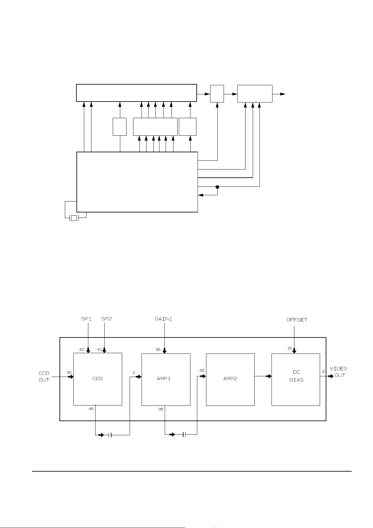
6. Analog processing IC (MN2038FAQ)
After eliminating the noise (CDS) from the CCD output signal (which is input to Pin39, to DS1/DS2 signal
of TG), Analog processing IC outputs it to Pin 46, and then it is input to pin 2 through C232 (for Row Clip and
primary amplificationAGC). Then it is output to Pin 35 and Pin 37 of EVR (IC206), which is input to pin 36,
which controls AGC. Pin 35 output signal is input to Pin 26 through C218, and is amplified second time at the
main amplifier. The offset adjust (pin 16 input) is activated by EVR output signal (Pin 4) and the output (Pin 21)
is sent to A/D converter.
Fig. 2-4
2-4 Samsung Electronics
Reference Information
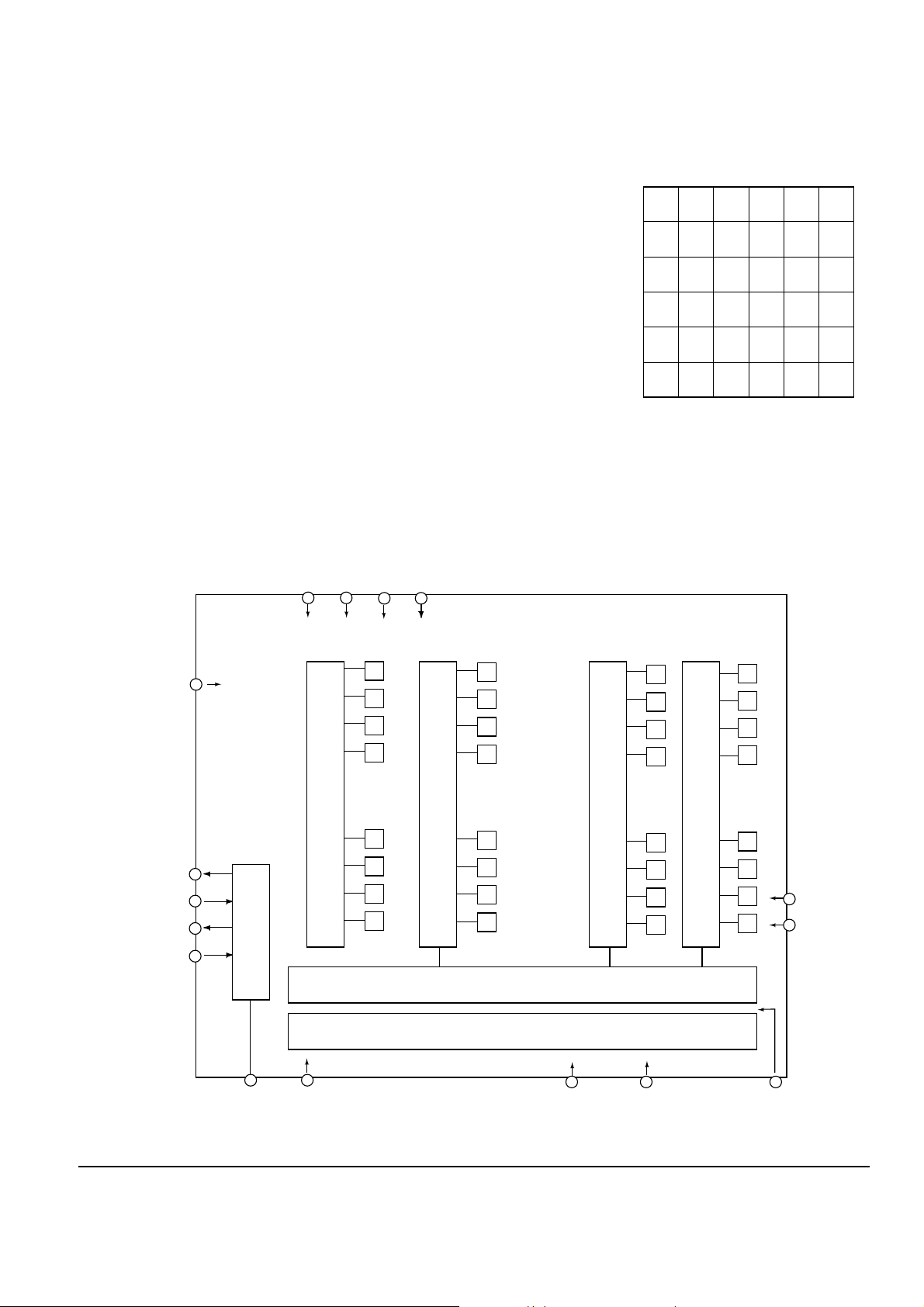
7. A/D converter (KAD0228) and DRAM Controller (SMA9606)
A/D converter converts the analog signal which is output from Analog processing IC to the 8-bit digital signal
(24.54Mhz). DRAM Controller is synchronized with Vsync, converts the 8-bit data which is output from A/D
converter to 16-bit data, and stores it in DRAM (controlled by the 32-bit microprocessor).
TRI
STATE
OUTPUT
(High Z
when
Power Off)
D_OUT(15:0)
–
RAS
CASU
CASL
WR
OE
A–OUT(9:1)
SO
SCK
SI
MODE
Data Register
&
SIO
SCS
AE Data Detect.
2 & Knee,
8bit to 16bit Convert
AD_IN(9:0)
–
ADCK IN(12.27MHz)
WND1 OUT
–
WND2 OUT
–
–
–
–
DRAM
Address
Generator
VD/HD
GEN
EXT VD IN
EXT HD IN
CLK IN(24.54MHz)
EOC
–
H ADJ
V ADJ
R/B
–
BREQ
–
BACK
–
Samsung Electronics 2-5
ADDR/DATA
BUS
CONTROL
Fig. 2-5
OE
–
 Loading...