How it Works
Log In / Sign Up
Buy Points
How it Works
FAQ
Contact Us
Questions and Suggestions
Users
Samsung
Loading...
S
SD604
4
SD604F
sd606
12
sd608
12
SD-616B
2
SD-616E
13
SD-616EEPS
SD-616F
2
SD-616Q
11
SD-616QEP
SD-616T
2
SD-816
2
SD-816B
6
SD-8550
9
SD-9420
2
SD-9420S32
SD-9421
3
SD9422
2
SD9450
2
SD-9451
SD9452
2
SD-9480
SD-9480H3W
SD9481
2
SDB-100
SDC-007
11
SDC-100
11
SDC14079
SDC14709
6
SDC14719
SDC16709
4
SDC16809
4
SDC17709
SDC18809
6
SDC18819
SDC1A809
5
SDC1H709
SDC1H719
SD-C21809
4
SDC-241
SDC-241 SERIES
SDC-243NA
SDC-243ND
SDC-243PA
SDC-243PD
SDC-243 SERIES
SDC-30
SDC-311
SDC-311 SERIES
SDC-313
SDC-313ANA
SDC-313AND
SDC-313APA
SDC-313APD
SDC-313A Series
SDC-313B
SDC-313NA
SDC-313ND
SDC-313PA
SDC-313PD
SDC-313 SERIES
SDC-33
15
SDC35701
2
SDC35711
SDC39801
2
SDC3B701
SDC3B701SDC35701
SDC3C801
6
SDC3C801/XEF
SDC-415
SDC-415 Series
2
SDC-425
SDC-425N
SDC-425ND
SDC-425P
SDC-425PD
SDC-425PH
SDC-435
2
SDC-435U
SDC-5340BC
2
SDC-7310DC
SDC-7310DCN
SDC-7310DCP
SDC-7340BC
3
SDC-7340BCN
2
SDC-7340BCP
2
SDC-7440DC
SDC-80
Sdc-80b
SDC-80T
10
SDC-89440BF
SDC-9410DU
SDC-9440BU
SDC-9441BC
SDC-9442DC
SDC-9443BC
2
SDC-K50
SDC-K60R
SDC-K65S
SDC-MS61S
Loading...
Loading...
Nothing found
SDC-33
Alignment and Adjustments
12 pgs
370.29 Kb
0
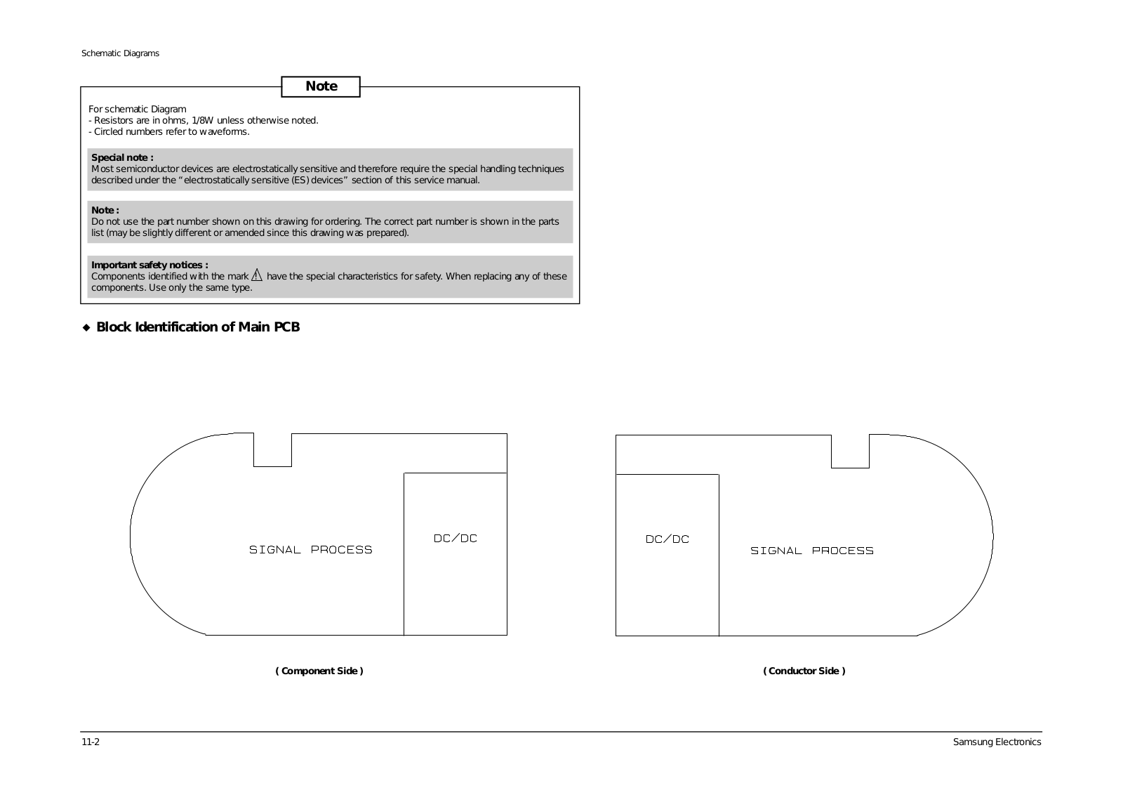
Block Diagram
1 pgs
238.43 Kb
0
Disassemble
6 pgs
562.67 Kb
0
Electrical Parts List
8 pgs
72.11 Kb
0
Expoioded View and Parts List
4 pgs
218.92 Kb
0
PCB Diagram
3 pgs
328.11 Kb
0
Precautions
2 pgs
149.82 Kb
0
Reference Information
16 pgs
561.32 Kb
0
Schematics Diagram
6 pgs
900.33 Kb
0
Service Manual
71 pgs
2.99 Mb
0
Service Manual
1 pgs
46.42 Kb
0
Specifications
2 pgs
72.12 Kb
0
Troubleshooting
10 pgs
261.1 Kb
0
User Manual
38 pgs
2.83 Mb
0
Service Manual
71 pgs
3.15 Mb
0
Table of contents
Loading...
Samsung Sdc-33 Schematics Diagram
...
Samsung Schematics Diagram
Download
Specifications and Main Features
Frequently Asked Questions
User Manual
Download
Loading...
+
4
hidden pages
Unhide
You need points to download manuals.
1 point = 1 manual.
You can buy points or you can get point for every manual you upload.
Buy points
Upload your manuals