

SAMSUNG SDC33 Service Manual
DIGITAL STILL CAMERA
SDC-30
SDC-33
SERVICE
POWER
MODE
TIMER
DELETE
1. Precautions
2. Reference Information
3. Product Specifications
4. Disassembly and Reassembly
5. Alignment and Adjustment
6. Troubleshooting
7. Exploded View and Parts List
8. Electrical Parts List
9. Block Diagram
10. PCB Diagrams
11. Schematic Diagrams
Manual
DIGITAL STILL CAMERA CONTENTS
© Samsung Electronics Co., Ltd. JUN. 1997 AD68-20286A / AD68-20289A
1. Precautions
1. Be sure that all of the built-in protective devices are
replaced. Restore any missing protective shields.
2. When reinstalling the chassis and its assemblies, be
sure to restore all pretective devices, including :
control knobs and compartment covers.
3. Make sure that there are no cabinet openings
through which people--particularly children
--might insert fingers and contact dangerous
voltages. Such openings include the spacing
between the picture tube and the cabinet mask,
excessively wide cabinet ventilation slots, and
improperly fitted back covers.
If the measured resistance is less than 1.0 megohm
or greater than 5.2 megohms, an abnormality exists
that must be corrected before the unit is returned
to the customer.
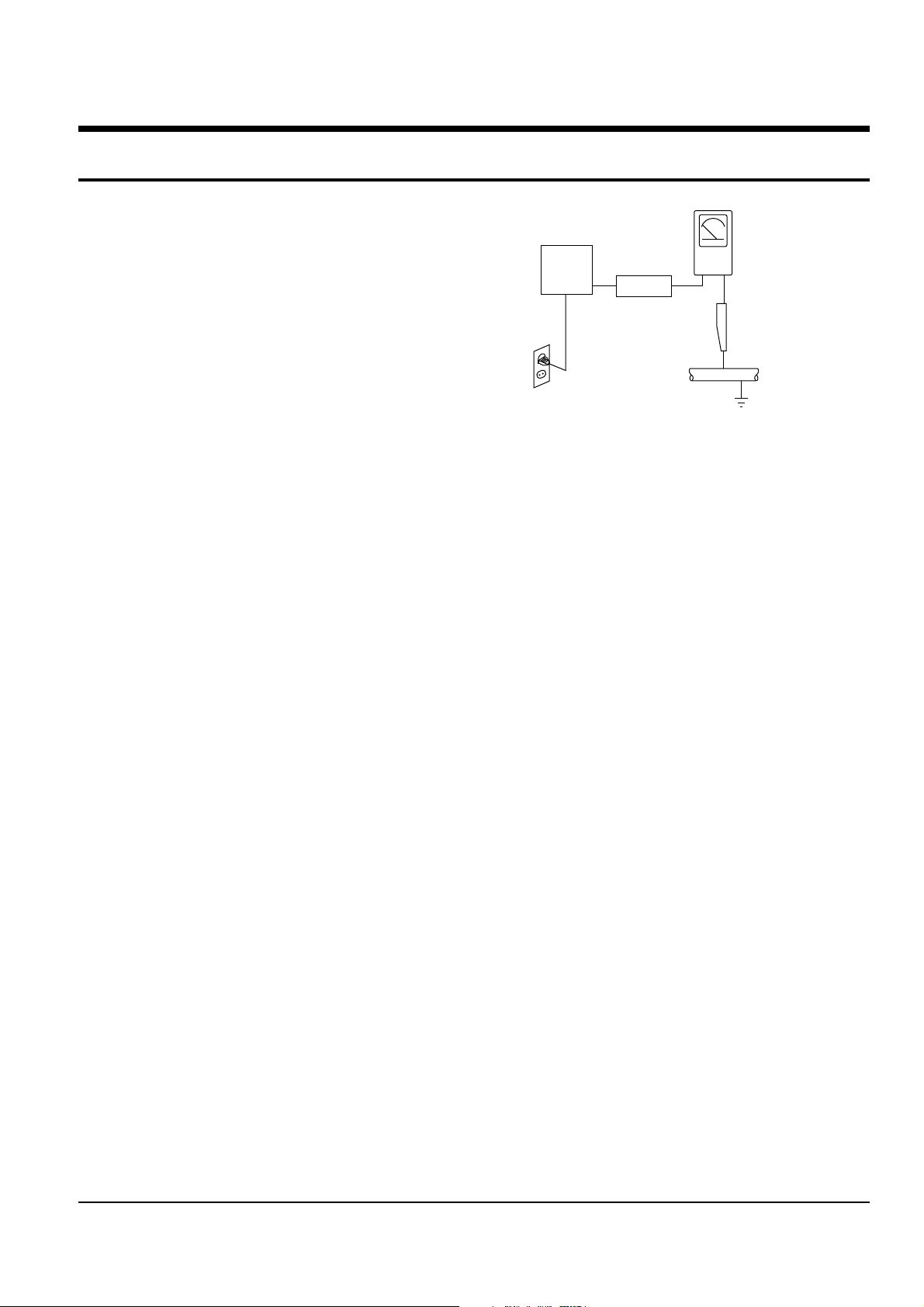
4. Leakage Current Hot Check (See Fig. 1) :
Warning : Do not use an isolation transformer
during this test. Use a leakage current tester or a
metering system that complies with American
National Standards Institute (ANSI C101.1,
Leakage Current for Appliances), and Underwriters
Laboratories (UL Publication UL1410, 59.7).
(Reading should
not be above
Device
Under
Test
Test all
exposed metal
surfaces
2-Wire Cord
Also test with
plug reversed
(using AC adapter
plug as required)
0.5mA)
Leakage
Currant
Tester
Earth
Ground
Fig. 1 AC Leakage Test
7. Antenna Cold Check :
With the unit’s AC plug disconnected from the
AC source, connect an electrical jumper across the
two AC prongs. Connect one lead of the ohmmeter
to an AC prong.
Connect the other lead to the coaxial connector.
8. High Voltage Limit :
High voltage must be measured each time
servicing is done on the B+, horizontal deflection
or high voltage circuits.
5. With the unit completely reassembled, plug the AC
line cord directly the power outlet. With the unit’s
AC switch first in the ON position and then OFF,
measure the current between a known erath
ground (metal water pipe, conduit, etc.) and all
exposed metal parts, including : antennas, handle
brackets, metal cabinets, screwheads and control
shafts. The current measured should not exceed
0.5 milliamp. Reverse the power-plug prongs in the
AC outlet and repeat the test.
6. X-ray Limits :
The picture tube is designed to prohibit X-ray
emissions. To ensure continued X-ray protection,
replace the picture tube only with one that is the
same type as the original.
Heed the high voltage limits. These include the
X-ray protection Specifications Label, and the
Product Safety and X-ray Warning Note on the
service data schematic.
9. Some semiconductor (“solid state”) devices are
easily damaged by static electricity.
Such components are called Electrostatically
Sensitive Devices (ESDs); examples include
integrated circuits and some field-effect transistors.
The following techniques will reduce the
occurrence of component damage caused by static
electricity.
10. Immediately before handling sny semiconductor
components or assemblies, drain the electrostatic
charge from your body by touching a known
earth ground. Alternatively, wear a discharging
Wrist-strap device. (Be sure to remove it prior to
applying power--this is an electric shock
precaution.)
Samsung Electronics 1-1

Precautions
11. High voltage is maintained within specified limits
by close-tolerance, safety-related components and
adjustments. If the high voltage exceeds the
specified limits, check each of the special
components.
12. Design Alteration Warning :
Never alter or add to the mechanical or electrical
design of this unit. Example : Do not add
auxiliary audio or video connectors. Such
alterations might create a safety hazard. Also, any
design changes or additions will void the
manufacturer’s warranty.
13. Hot Chassis Warning :
Some TV receiver chassis are electrically
connected directly to one conductor of the AC
power cord. If an isolation transformer is not
used, these units may be safely serviced only if
the AC power plug is inserted so that the chassis
is connected to the ground side of the AC source.
To confirm that the AC power plug is inserted
correctly, do the following : Using an AC
voltmeter, measure the voltage between the
chassis and a known earth ground. If the reading
is greater than 1.0V, remove the AC power plug,
reverse its polarity and reinsert. Re-measure the
voltage between the chassis and ground.
14. Some TV chassis are designed to operate with 85
volts AC between chassis and ground, regardless
of the AC plug polarity. These units can be safely
serviced only if an isolation transformer inserted
between the receiver and the power source.
18. Picture Tube Implosion Warning :
The picture tube in this receiver employs
“integral implosion” protection. To ensure
continued implosion protection, make sure that
the replacement picture tube is the same as the
original.
19. Do not remove, install or handle the picture tube
without first putting on shatterproof goggles
equipped with side shields. Never handle the
picture tube by its neck. Some “in-line” picture
tubes are equipped with a permanently attached
deflection yoke; do not try to remove such
“permanently attached” yokes from the picture
tube.
20. Product Safety Notice :
Some electrical and mechanical parts have special
safety-related characteristics which might not be
obvious from visual inspection. These safety
features and the protection they give might be
lost if the replacement component differs from the
original--even if the replacement is rated for
higher voltage, wattage, etc.
Components that are critical for safety are
indicated in the circuit diagram by shading,
( or ).
Use replacement components that have the same
ratings, especially for flame resistance and
dielectric strength specifications. A replacement
part that does not have the same safety
characteristics as the original might create shock,
fire or other hazards.
15. Never defeat any of the B+ voltage interlocks.
Do not apply AC power to the unit (or any of its
assemblies) unless all solid-state heat sinks are
correctly installed.
16. Always connect a test instrument’s ground lead to
the instrument chassis ground before connecting
the positive lead; always remove the instrument’s
ground lead last.
17. Observe the original lead dress, especially near
the following areas : Antenna wiring, sharp
edges, and especially the AC and high voltage
power supplies. Always inspect for pinched, outof-place, or frayed wiring. Do not change the
spacing between components and the printed
circuit board. Check the AC power cord for
damage. Make sure that leads and components
do not touch thermally hot parts.
1-2 Samsung Electronics

2. Reference Information
2-1 Circuit description
2-1-1 DSC
Digital camera(SDC-30/33), is an image-input device that connects to a PC. It’s small and light welght, supplies
high quality images and has a large capacity (4MB/2MB). The digital camera consists of 3 sections: Camera,
signal processing and storage.
1. Camera
The camera is similar to a camcorder but adapts a scanning method of 525/30 (which can read an entire image of
in one frame, whereas the camcorder’s scanning method is 525/60.
Photo-exposure is controlled by the electronic shutter through timing generator and CCD driver IC (where as a
camcorder controls the exposure using an IRIS).
Main function of this part is to control the photo-exposure in accordance with the brightness, and to store the
image in DRAM.
2. Digital Signal Processing
Image information of 1 frame is temporarily stored in DRAM. Image information stored in DRAM is the
digitalized CCD signal from the camera. It needs additional image signal processing by the 32-bit microprocessor.
The image signal processing done by the microprocessor includes white balance, shape adjustment and Y/C
signal conversion.
3. Storage
After image signal processing, an image signal compression technique allows more image to be stored in the
limited memory. In the case of SDC-30/33, 10:1 compression is normally executed for standard JPEG specification.
After compression, the image information is stored in the nonvolatile flash memory : Max. 45/22 frame for
VGA(640*480), and max 180/90 frame for QVGA(320*240).
The image can be stored, edited, and printed by the PC image editing program that is supplied with the camera.
2-1-2 Power
LCD MICOM generates the control signal that turns on the system (5V). When the power is on, the signal turns
on IC140 PWM IC which outputs 5V through T141.
When shot key is pressed, the signal for output is generated from MICOM, which turns on IC120 PWM IC and
outputs 5V, -7V, and 15V through T121. After the shot, the camera control signal turns off the power supply within. 5sec (through T121).
2-1-3 DC/DC block operation description
2-1-3(A) DC/DC BLOCK CONSISTS OF THREE COMPONENTS AS BELOW.
1. EVER5V
EVER5V consists of S8420 (IC100) IC and the assocciat battery circuitry (CN101 Pin2) is input to
IC100 (S8420). Pin 8 and 5V voltage are generated internally and are output to pins 1 and 7. EVER5V power
(Pin 1) is input to the function board for LCD MICOM (IC601) drive, POWER S/W (LED01) driving power, and
PULL-UPvoltage. RESET output of IC100 Pin 5, which changes from low to high at the power input, is connected
to LCD MICOM RESET PIN (and resets LCD MICOM).
Samsung Electronics 2-1
Reference Information
2. Camera power
Camera power block consists of IC120 (PWM IC MB3800), Q121 (INVERTER TR DTC144EU), Q122 (SWITCHING TR KSD1621), and rectifier circuit.
When CAM5V control pin of LCD MICOM 10PIN is high, it is converted at Q121 and IC 120. Pin 4 becomes low;
then IC120 Pin 7 starts oscillating and the PWM output from IC120 Pin 5 switches Q122. Pin 6 generates the 15V
output by a switching pulse and this output is rectified by D121, L123, C127, and C128 to generate 15V power for
the drive of CCD (IC201) and V DRIVE IC (MN3112SA).
The pulse for -7V (which is generated at T121 pin 10), is rectified by D121, C129, L124, C130 and becomes -7V
power for the drive of CCD and V DRIVE IC.
The pulse for 5V power, which is output from T121 pin 7, becomes CAMERA 5V power by D122, C133, L127, and
C134. The 5V power is divided by D5V for the drive of IC204(MN5246) and IC202(MN3112SA) and A5V for the
drive of IC203, IC205, and IC206 through L125.
3. SYS 5V
Using the same technique as with camera 5V (L141, IC140, Q142, and T141), the SYS 5V power drives IC301,
IC302, IC303, IC304 and IC307, and is generated by SYS 5V CONT from the LCD micom.
EVER5V power is always output when battery and adapter are connected; SYS 5V power is output only when
power is turned on. CAM power is output for 0.5 second (only during shot operation).
2-1-4 Camera
1/3" 35
CCD
LENS
V-Drive
1. Camera operation
V1~V4
VSUB
CDS out
Vout Vout
R
H1
H2
Timing
AGC IN
CDS
AGC
SMD
SHP
Gen
A/D
(8bit)
D Data, DCLK
HD, VD
Fig. 2-1
D7~D0
Data 8
8-16 CONV.
DRAM CTRL
Camera
Ctrl
D15~D0
Data 16
16
DRAM
4Mb
Address
A9~A1
S/W
DSCP
RISC Chip
The image from the lens is converted to an electrical signal by the photoelectric conversion component, CCD
(MN3776PE). Each pulse used to extract CCD signal is generated by the timing geneartor IC(MN5246),
converted to actual driving voltage by V Drive IC(MN3112SA), and supplied to CCD. After noise elimination
(CDS) and amplification (AGC) at analog process IC(NN2038FAQ), CCD output signal is converted to a digital
signal by A/D converter. The 8-bit digital data is changed to 16-bit by DRAM control IC(SMA9606), and stored in
the DRAM.
2-2 Samsung Electronics
Reference Information
2. Lens
SDC-30/33 lens uses a fixed focus method, and can take a photograph clearly at over 1 meter distance (optimal
quality is between 1.5 and 3 meters).
3. Color Filter
Color filter, which remove, the color information on CCD, adapts RGB method
for best color characteristics and Bayer method for best.
RGRG – –
GBGB – –
RGRG – –
4. CCD(MN3776PE) and V Driver(MN3112SA)
GBGB – –
CCD converts the optical image to an electrical signal and is similar to an
existing camcorder (except for the scanning method). The camcorder method
––––––
uses interlace scanning, which outputs a field image every 1/60 second. (First
field consists of odd lines, the second field consists of even line, and a complete
––––––
picture consists of two fields. However, SDC-30/33 uses a the progressive
scanning method, which outputs a frame every 1/30 second (and has excellent vertical resolution).
The image is output at Pin 1 of CCD, and is input to Pin39 of analog signal process IC (IC203) through TR (Q201).
V Driver IC (MN3112SA) mixes each CCD driving pulse from Timing Generator IC, and converts it to
the required voltage.
Effective Pixel
325,546=659(H)X494(V)
ØV1~ØV4: Vertical Shift Clock
ØH1~ØH2:
Horizontal Shift Clock
V01: Video output
Ø
V
1
15 13
<BLOCK>
Ø
Ø
Ø
Ø
V
V
V
V
3
2
4
14 12
P W
V O 1
(Bias) L G
V O 2
O D
16
1
2
5
4
3
V
e
r
t
i
c
a
l
S
h
i
f
t
R
e
g
i
s
t
e
r
9
S U B
11
P T
Horizontal Shift Register 1
Horizontal Shift Register 2
6
O GØ R
7810
S GØ H 2Ø H 1
Fig. 2-2
Samsung Electronics 2-3
Reference Information
5. Timing Generator (MN5246)
A timing generator generates each clock, synchronized signal, and CCD driving pulse for the system. Also, it
receives the shutter speed information for the photo-exposure control (from the microprocessor).
Signal
process
CLK
VDO,HDO
CSYNC
Image signal
H1
H2
bias
CCD
ØV2
ØV1
V1RV2V3V4
ØV3
ØV4
SUB
ØSUB
CH1
CDS
ØSG
DS1,DS2
SG
MN 5246
VDLIDE
2fck=24.5Mhz
Fig. 2-3
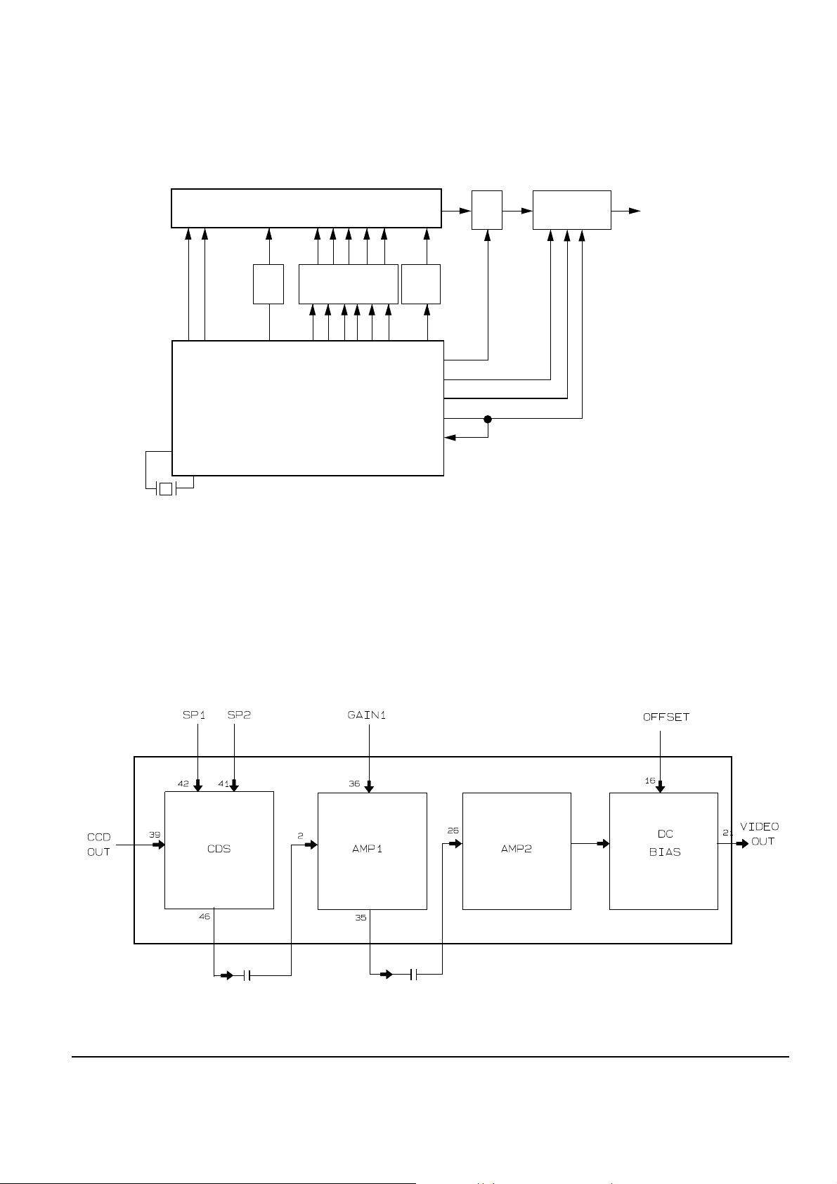
6. Analog processing IC (MN2038FAQ)
After eliminating the noise (CDS) from the CCD output signal (which is input to Pin39, to DS1/DS2 signal
of TG), Analog processing IC outputs it to Pin 46, and then it is input to pin 2 through C232 (for Row Clip and
primary amplificationAGC). Then it is output to Pin 35 and Pin 37 of EVR (IC206), which is input to pin 36,
which controls AGC. Pin 35 output signal is input to Pin 26 through C218, and is amplified second time at the
main amplifier. The offset adjust (pin 16 input) is activated by EVR output signal (Pin 4) and the output (Pin 21)
is sent to A/D converter.
Fig. 2-4
2-4 Samsung Electronics
Reference Information
7. A/D converter (KAD0228) and DRAM Controller (SMA9606)
A/D converter converts the analog signal which is output from Analog processing IC to the 8-bit digital signal
(24.54Mhz). DRAM Controller is synchronized with Vsync, converts the 8-bit data which is output from A/D
converter to 16-bit data, and stores it in DRAM (controlled by the 32-bit microprocessor).
TRI
STATE
OUTPUT
(High Z
when
Power Off)
D_OUT(15:0)
–
RAS
CASU
CASL
WR
OE
A–OUT(9:1)
SO
SCK
SI
MODE
Data Register
&
SIO
SCS
AE Data Detect.
2 & Knee,
8bit to 16bit Convert
AD_IN(9:0)
–
ADCK IN(12.27MHz)
WND1 OUT
–
WND2 OUT
–
–
–
–
DRAM
Address
Generator
VD/HD
GEN
EXT VD IN
EXT HD IN
CLK IN(24.54MHz)
EOC
–
H ADJ
V ADJ
R/B
–
BREQ
–
BACK
–
Samsung Electronics 2-5
ADDR/DATA
BUS
CONTROL
Fig. 2-5
OE
–
Reference Information
2-1-5 Digital Section
1. Overview
8-6 CONV
DRAM CTRL
Camera
Ctrl
S/W
DSCP
DRAM
4Mb
32bit RISC MICROPROCESSOR
Power
Control
S/W
JPEG
LCD
Micom
Flash
Memory
16Mb/32Mb
Memory
Pannel
Ctrl
PC I/F
LCD
Fig. 2-6
2. DRAM (KM416C256BLT) and flash memory (TC5832FT/TC5816FT)
DRAM stores the image signal temporarily and enables the microprocessor to process the signal. Flash memory
(nonvolatile) records various system information and the compressed image.
3. 32-bit RISC microprocessor (HD6477043F28)
This microprocessor is the core of the system and handles the camera control, image signal processing, image
compression, flash memory control, communication with PC, and communication with LCD control MICOM.
(Refer to 2-1-6 “System Control” for details.)
2-6 Samsung Electronics
Reference Information
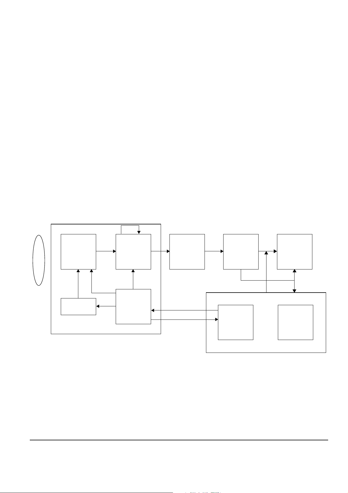
2-1-6 Sytem control
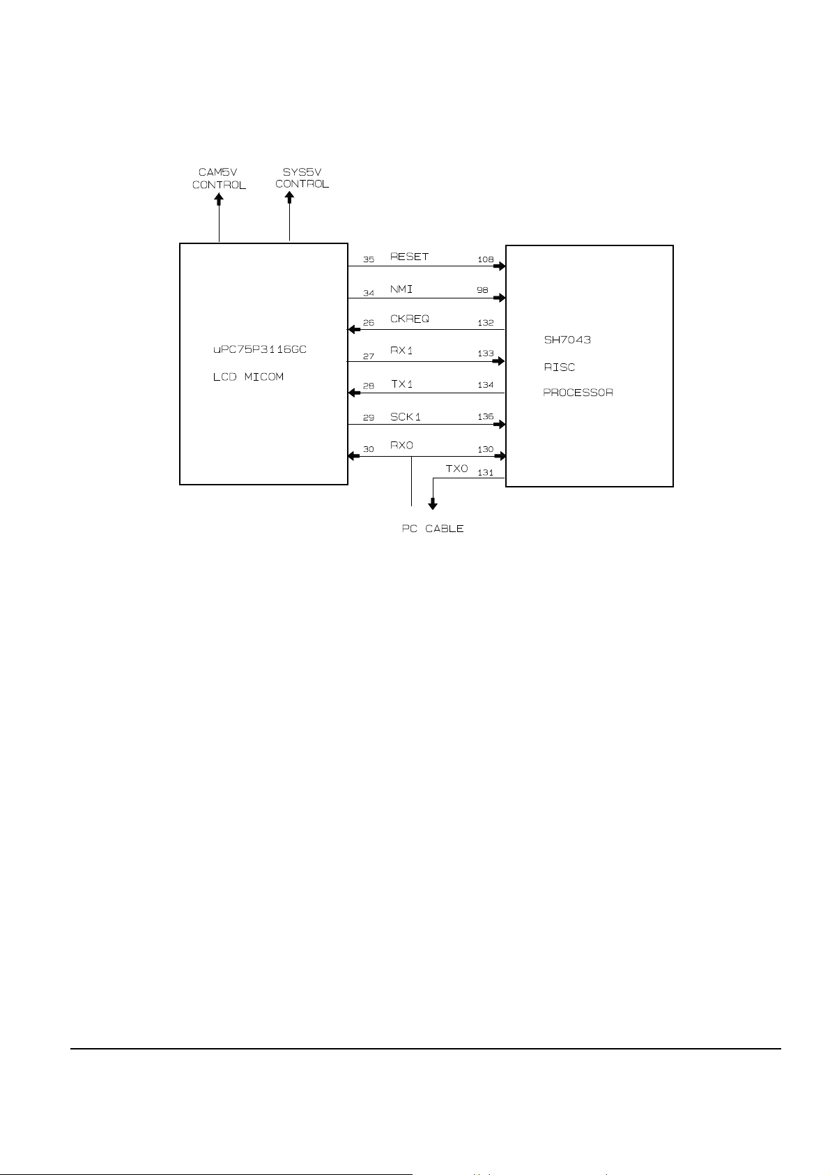
Dual controller (MICOM) is located in DSC : A RISC chip controls the signal processing, and is the 4-bit MICOM
controls the LCD, timer, and switch.
Fig. 2-7
1. 4-bit MICOM; Functions and connections
1) PIN connection status
- RISC is connected to the 4-bit MICOM (total 7 lines).
- Pins 98, 130, and 108 and SCI No. 1 are used.
- Pins 132, 133, 134, and 136 are used for communication with 4-bit MICOM.
- Synchronized communication is used with 4-bit MICOM.
2) Function
- RISC is usally in the standby mode (low-power) because it consumes so much current when it operates.
- 4-bit MICOM acknowledges the starting time (for example, when the user pushes the shot key) and sends the
NMI pin signal to RISC, so that the standby mode can be changed to the operation mode. The information is
sent to RISC through communication port. After RISC executes the appropriate program, it returns to the
standby mode.
2. Main function of 4-bit MICOM
- Power ON/OFF: 4-bit MICOM turns the PC (main body) on, and turns on the RISC.
- Execution of shot: When the shot is executed by the PC key (or main body), 4-bit MICOM signals the shot
execution to RISC. When the shot is finished (system 5V and head power 5V), 4-bit MICOM changes the RISC
mode to standby mode.
- Delay shot: When the delay shot is executed by the PC key (or main body), 4-bit MICOM signals the RISC and
supplies the system 5V and head power 5V. Then, the RISC changes to standby mode.
Samsung Electronics 2-7

Reference Information
- Mode change: When the mode is input by the PC key (or main body), 4-bit MICOM signals the RISC. When
the mode is changed, 4-bit MICOM displays it on LCD, and changes the RISC to standby mode.
- Delete execution: When the delete instruction is input by the PC key (or main body), 4-bit MICOM signal the
RISC and changes the RISC to standby mode.
- LCD display: DSC status is displayed.
- Error handling: When an error occurs, (or RISC) the error message is displayed on LCD. If the RISC cannot
operate, the power is automatically off.
- Battery operation: The capacity of battery is classified as "Full", "Half", "Low", or "Battery replacement". For the
"Battery replacement" status, only the power on/off function is available, and other functions cannot operate.
- Auto power OFF: When any operation has not been executed (three minutes for main body operation, or
10 minutes for PC operation) the power automatically turns off.
3. Main functions of RISC processor
- Communication with 4-bit MICOM: RISC operation is completely controlled by the 4-bit MICOM.
A synchronization method is adapted for communication between 4-bit MICOM and RISC (with 8-bit*11 byte
communication).
- DRAM control: RISC processor includes internal BSC. BSC helps RISC to control the DRAM. RISC uses DRAM
as though it were internal RAM (with the help of BSC). BSC generates all DRAM control signals by itself. RISC
uses DRAM for the image buffer, temp memory for the calculation, and an area that manages the flash
memory and FAT(File Allocation Table).
- Camera Head control: RISC handles the control of the camera head during the shot. RISC controls the timing
generator, ASIC, etc. so that the image data from CCD can be transferred.
- Signal processing: RISC executes the signaling processing internally with CCD image data stored in DRAM.
After RISC separates CCD data into RGB, and processes detail and gamma, it creates a YUV signal, and
executes JPEG compression. The compressed JPEG data will be stored in DRAM again.
- Flash memory control: The compressed data (in DRAM) is stored in the flash memory. The file management
program is recorded in RISC, and manages the files in the flash memory (file location, file size, etc).
- PC communication: RISC processor receives the signal from PC (4-bit MICOM) and activates up RISC.
Then, RISC processor sets the flag for the request input from PC, and transfers the flag to RISC. The RISC
communicates with PC through the serial port. (PC always requests the PC communication to DSC, but RISC
does not request it from the PC.)
- Battery level checking: Battery indicator, which is displayed in LCD of 4-bit MICOM, accepts the data from
RISC. Battery level checking is executed when the camera head and main board are on. When new battery is
inserted, it outputs 6.2V; but the actual voltage drops below 6V after supplying power to the camera head and
main board.
2-8 Samsung Electronics
2-2 IC Blocks
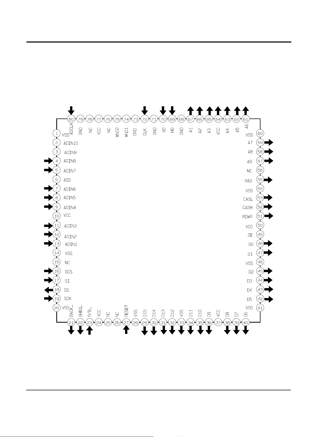
2-2-1 IC301 (SMA9606)
Reference Information
Samsung Electronics 2-9
Reference Information
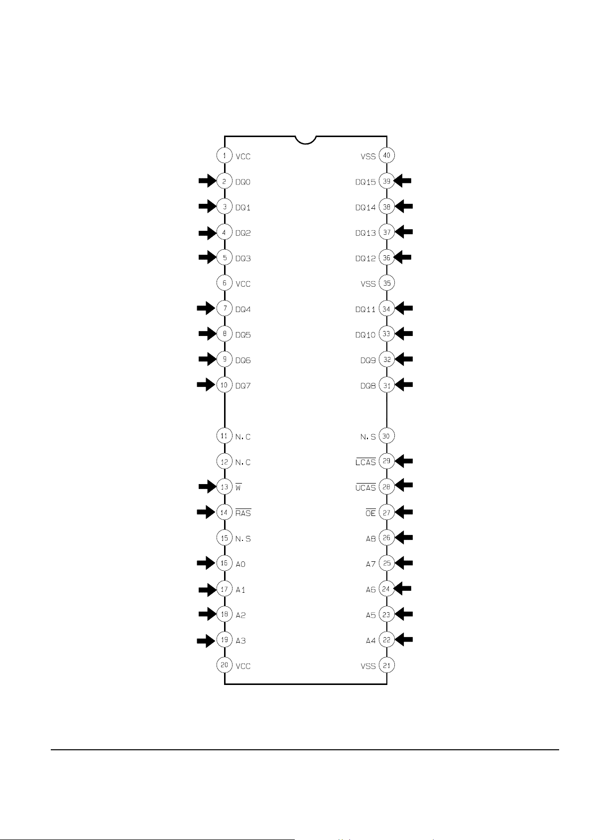
2-2-2 IC302 (KM416C256BLT)
2-10 Samsung Electronics
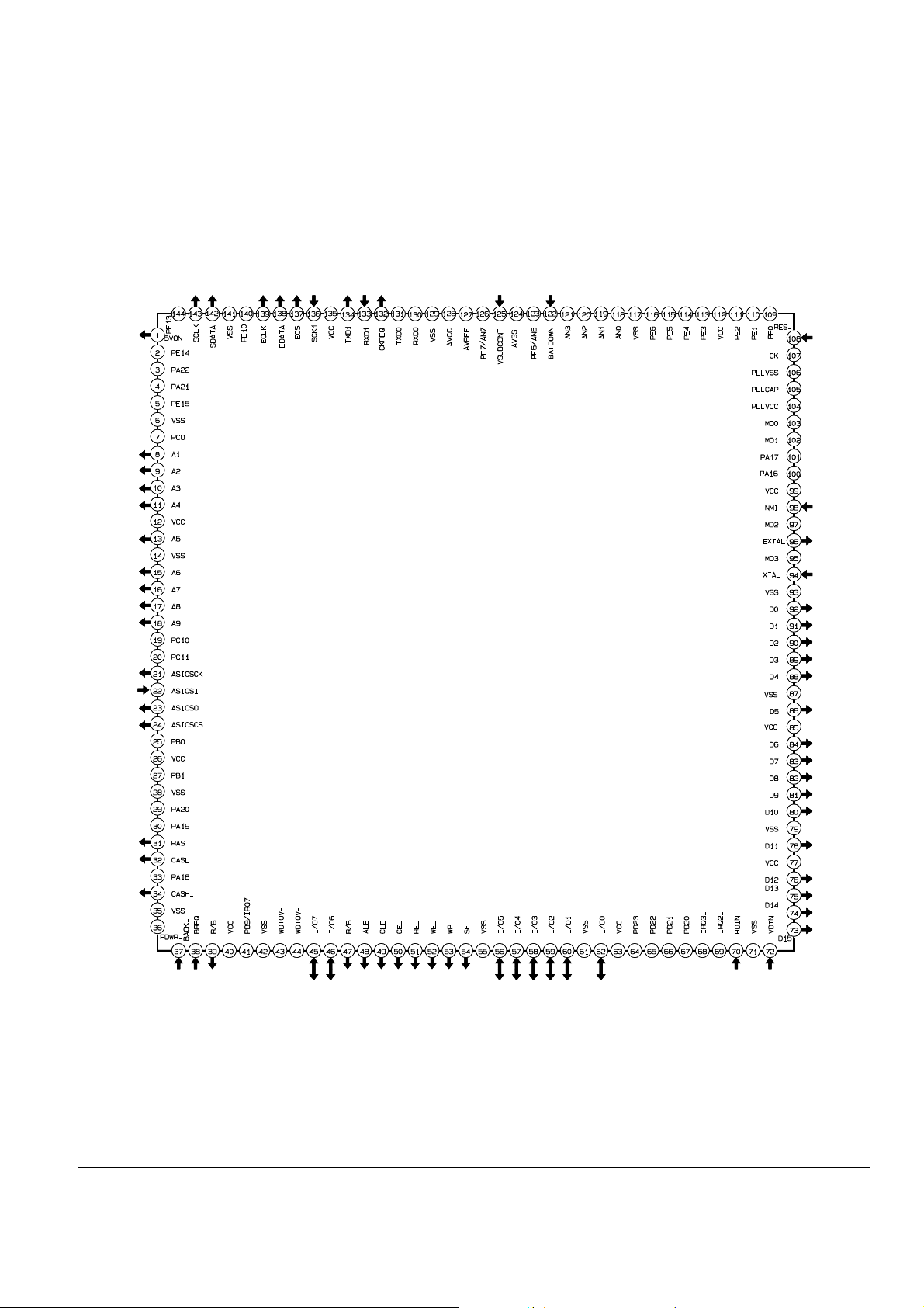
2-2-3 IC304 (HD6477043)
Reference Information
Samsung Electronics 2-11
Reference Information
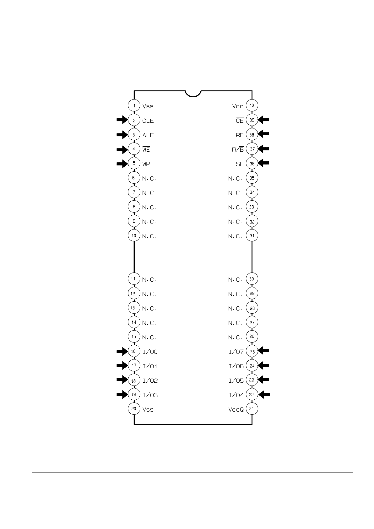
2-2-4 IC307 (TC5832FT)
2-12 Samsung Electronics
2-2-5 IC601 (UPD75P3116GC)
Reference Information
2-2-6 IC501 (MAX232C)
Samsung Electronics 2-13
Reference Information
2-2-7 IC203 (NN2038FAQ)
2-14 Samsung Electronics

2-2-8 IC204 (NN5248)
Reference Information
Samsung Electronics 2-15

Reference Information
MEMO
2-16 Samsung Electronics

3. Product Specifications
Design and specifications are subject to change without notice.
Operation
SDC-30 SDC-33
Descriptions
Image sensor
Color depth
Memory
Image capacity
Compression
Lens
Range
Viewfinder
Shutter
Exposure system
Color balance
Sensitivity
Picture formats
Supported OS
PC
requirements
PC lnterface
Image transfer
time (speed)
Power
Power
consumption
Battery life
Dimensions
Net weight
350,000 pixel CCD
(STD) :640 X 480 pixels (ECO)20 X 240 pixels
24 bit true color (16million colors)
2MB internal flash memory
Standard (STD) : 22 images
Economical (ECO) : 88 images
Standard JPEG
Fixed focusing
100 cm (3.3 feet) - infinity
Separate optical
Auto electronic (1/4 ~ 1/8000 seccond)
Auto exposure
Automatic White Balance (AWB)
ISO 100
BMP, JPG, PCX, PNG
PSD, TGA, TIF, TPL
Windows 3.1 or higher (Including Windows 95)
RAM : 8MB or more
HDD : 30MB or more (free space)
CPU : 486DX or higher (IBM PC based)
CD- ROM drive (recommended)
Standard RS-232C (9600 -115200bps)
(STD) Standard images : 7~8 sec. (at 115Kbps)
(ECO) Economy images : Under 2 sec. (at 115Kbps)
4AA TYPE alkaline batteries
6V DC in using AC adaptor (not supplied)
At power on : below 500mA
At power off : below 500uA
More than 200 images using new alkaline batteries
115(W) X 75(H) X 38(D)mm
140g (without batteries)
350,000 pixel CCD
(STD) :640 X 480 pixels (ECO) : 320 X 240 pixels
24 bit true color (16million colors)
4MB internal flash memory
Standard (STD) : 45 images
Economical (ECO) : 180 images
Standard JPEG
Fixed focusing
100 cm (3.3 feet) - infinity
Sparate optical
Auto electronic (1/4 ~1/8000 seccond)
Auto exposure
Automatic White Balance (AWB)
ISO 100
BMP, JPG, PCX, PNG
PSD, TGA, TIF, TPL
Windows 3.1 or higher (Including Windows 95)
RAM : 8MB or more
HDD : 30MB or more (free space)
CPU : 486DX or higher (IBM PC based)
CD- ROM drive (recommended)
Standard RS -232C (9600 -115200bps)
(STD) Standard images : 7~8 sec. (at 115Kbps)
(ECO) Economy images : Under 2 sec. (at 115Kbps)
4AA TYPE allaline batteries
6V DC in using AC adaptor (not supplied)
At power on : below 500mA
At power off : below 500uA
More than 200 images using new alkaline batteries
115(W) X 75(H) X 38(D)mm
140g (without batteries)
Samsung Electronics 3-1

Product Specifications
MEMO
3-2 Samsung Electronics
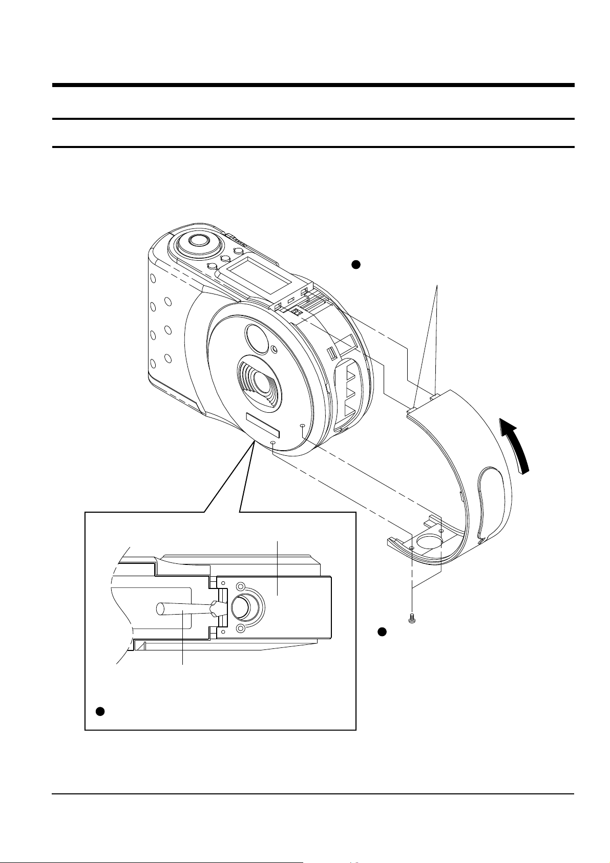
4. Disassembly and Reassembly
4-1 Cabinet and PCB
Disassemble in the order shown.
(Reassemble in reverse order.)
4-1-1 Case-Side Removal
3
Disconnect 2 tabs while lifting
up the case-side to the arrow direction.
Bottom Side
1
Remove 2 screws.
Precision screw Driver
2
Lift up the case-side using the precision screw driver.
<BOTTOM SIDE>
Fig. 1
Samsung Electronics 4-1
 Loading...