Page 1

Agenda
Agenda
Ⅰ. Introduction
Ⅱ. Main PBA
Ⅲ. OPE PBA
Ⅳ. SMPS PBA
Page 2

Objectives
Objectives
I. To make you aware of the
key specification points
II. To show you how SCX-4200
series are different
Page 3
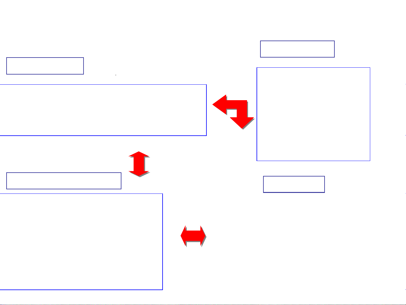
1-1. Overview
Panel Board
OPC
SMPS + HVPS
Main Board
Page 4
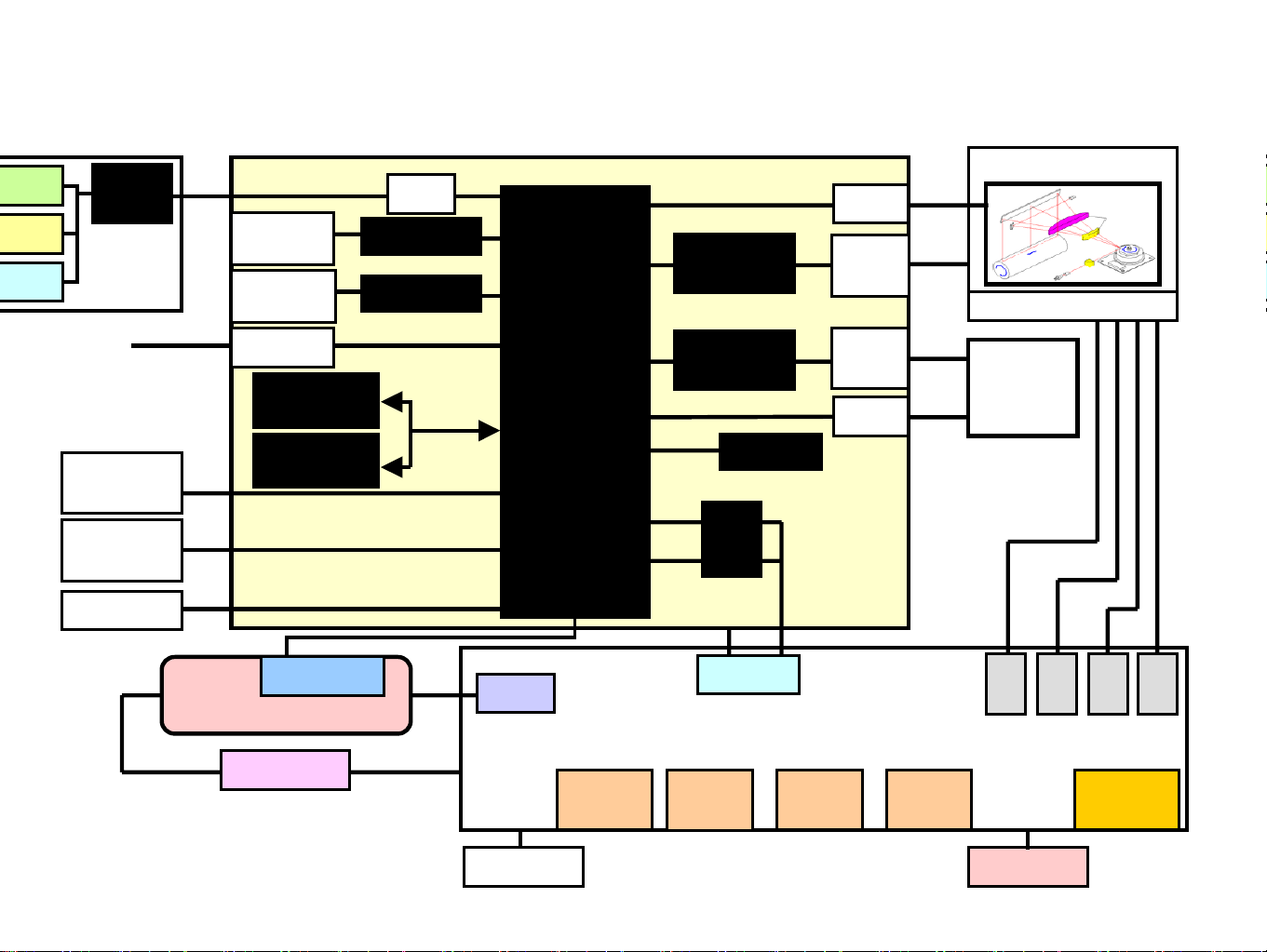
1-2. Block Diagram
LCD
KEY
LED
HC
48C50
OPE
Pickup
Solenoid
MP
Solenoid
Main CLK
10.00MHz
Video CLK
16.59MHz
USB2.0
FLASHROM
29LV800
SDRAM
8MB
UART
CY25811
CY25814
A(1:20)
D(0:15)
Chrous2
Main Board
Motor Drv.
A3977
Motor Drv.
A3977
3.3V
1.8V
3.3V
RESET IC
REG
REG
LSU
Main
Motor
Scan
Motor
CIS
Engine
Frame
Developer
Unit
Scanner
LSU
FAN 2
Thermistor
Fuser
Thermostat
TRIAC
FAN 1
P/Empty
Sensor
24V/5V
MP
Sensor
5V
SMPS
HVPS
Exit
Sensor
Feed
Sensor
T
R
CDRH S/W
S
R
D
R
Cover
Open S/W
C
R
Page 5

1-3. Connection Diagram
Page 6
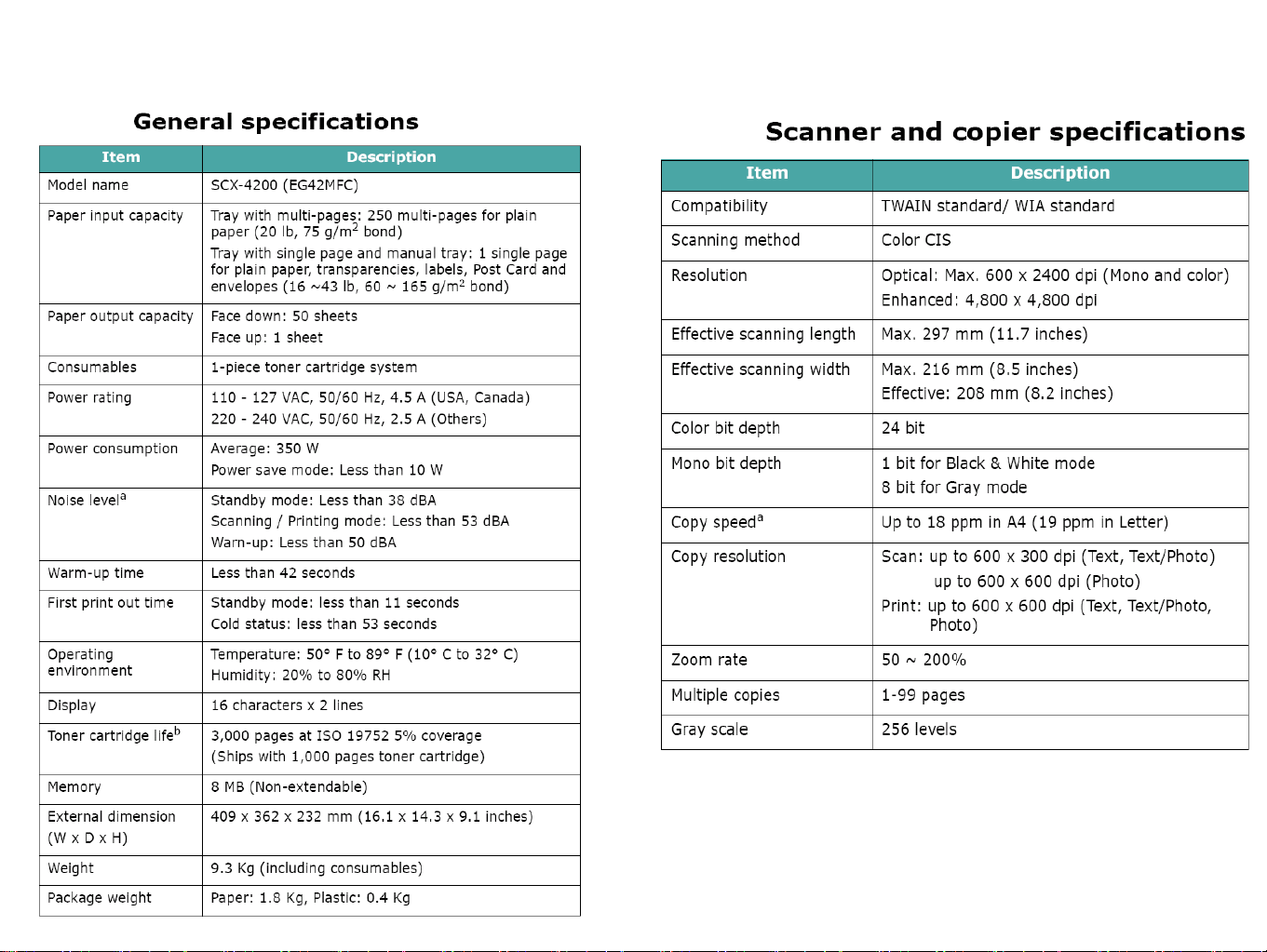
1-4. General Spec.
Page 7
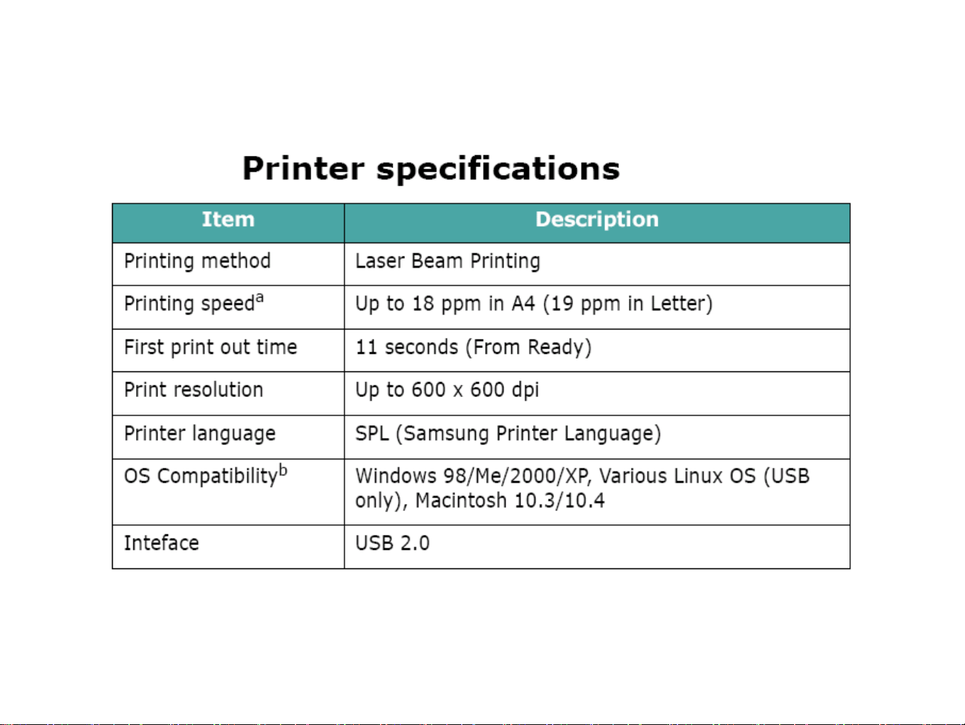
1-4. General Spec.
Page 8
1-5. Comparison Between SCX-4100 and SCX-4200
Same (Chorus 2)CPU
Same (1MB)ROM
Same (8MB)RAM
16.59MHz12.99MHzVideo Clock
USB 2.0USB 1.1USB
Main
2NK (Bi-polar)2K (Bi-Polar)Main-Motor
A3977AN44060Motor-IC
Same (600W)Heat-Lamp
SameLSU
Main(1) + Sub(1)Main(1)Fan
LITEON 600dpiCanon 600dpiCIS
ETCSCX-4200SCX-4100Item
Scan
Panel
SMPS
/HVPS
Bi-Polar(35Φ)Uni-Polar(35Φ)Scan-Motor
A3977 (Bi-polar)STA403A(Uni-Polar)Motor-IC
2*16 , 8Keys , 1LED2*16 , 7Keys LCD
48C05(Holtec)9228(SEC)ASIC
SameSMPS
SameHVPS
SMPS/HVPS on 1 Board
->Heat Sink Added
Page 9

Objectives
Objectives
I. To show you the structure
and key elements of Main
PBA in SCX-4200
Page 10

2-1. General description
Main PBA employs Chorus2 as an ASIC, which is developed for LBP Printer
1 32 4 15 67 8
20 219 7
10 11 12 135 17 18 191416
Page 11

2-1. General description
MAIN CLUTCH CONNECTOR3 (CN2)12LSU CONNECTOR (CN5)1
MAIN MOTOR DRIVER IC –A3977(U12)
2
SCAN MOTOR DRIVER IC –A3977 (U6)
5
MP CLUTCH CONNECTOR (CN3)11
FLASH ROM-29LV800 (U4)13
SDRAM -K4S641623H-TL75 (U2)14MAIN MOTOR CONNECOR (CN10)3
CIS CONNECTOR (CN8)15PTL CONNECTOR (CN9)4
GRAPHIC PROCESSOR ASIC-CHORUS2 (U5)16
MAIN CLOCK CRYSTAL-10.00 MHz (OSC3)17SCAN MOTOR CONNECTOR (CN13)6
VIDEO CLOCK CRYSTAL -16.59MHz (OSC2)18THERMISTOR CONNECTOR (CN12)7
19USB 2.0 (CN6)8
USB CLOCK CRYSTAL –12MHz (OSC1)
OPE CONNECTOR (CN14)20CRUM CONNECTOR (CN11)9
FAN2 (CN7)21ENGINE CONNECTOER (CN4)10
Page 12

2-2. LBP CPU Serises
CPU Core Clock Bus Package features
Jupiter 4e
SPGPm
SPGPv3
Chorus 2
Chorus m
PPC 266
RM7000Se
ARM 9 150㎒ 16 bit QFP Internal Flash 0.5MB
ARM 9 166㎒ 16 bit BGA RAM 32bit Control
ARM 10 400㎒ 32 bit BGA DDR Memory supporting
ARM 7 66㎒ 16 bit QFP Internal CIP
ARM 9 300㎒ 32 bit BGA Internal CIP
PPC 266㎒ 32 bit QFP CPU
MIPS 460㎒~ 64 bit BGA CPU
Page 13

2-3. Chorus2
Samsung's S3C46Q0X 16/32-bit RISC micro controller is designed to provide a cost-effective, low
power, small die size and high performance micro-controller solution for inkjet, laser beam printer and
MFP.
The S3C46Q0X is developed using ARM7TDMI core, 0.18m CMOS standard cell, and memory cell.
The integrated on-chip functions are as follows:
- 1.8V internal, 3.3V external (I/O boundary) microprocessor with 4KByte Cache
- Image Processor
- On-chip clock generator with PLL
- Memory & External Bank Control
- DMA Control (5-channel)
- Interrupt Control
- 2-port USB Host /1- port USB Device (ver 2.0) Interface Control
- UART (2 Channel)
- Synchronous Serial Interface Control
-Timer (4 Channel)
- Watch Dog Timer
- Power control: Normal, Slow, Idle, Stop and SL_IDLE mode
- A/D Converter (10-bit, 2 Channel)
- General I/O Port Control
- Print Head Control
- Carrier Motor Control
- Paper Motor Control
- Tone Generator
- RTC with calendar function
- S/W Assistant function( Rotator )
Page 14

Ⅱ. Main PBA
2-3. CPU (Chorus2)
Boundary Scan
JTAG
ARM7TDM
Clock Generator
(MPLL)
Clock Generator
(UPLL)
Clock Generator
(PPLL)
Controller
AIN[3:0]
I
TAP
10bit ADC
Watchdog Timer
(Real Time Clock)
Block diagram
CPU Unit
Write
Buffer
ARM7TDMI
CPU Core
Cache
4K Byte
System Bus Bridge & Arbitration /
Rotator
RTC
SSB
BDMA (2-Ch.)
Bus Arbiter
Memory I/F ROM/
SRAM
DRAM/SDRAM
PRT_TOP
Interrupt
Controller
General DMA
(2-CH)
I
P_TOP
USB v1.1
GPIO
Controller
System Timer
(4-ch)
UART (2-ch)
HP SIO
Tone Generator
CRCON
LFCON
CRFIRE
LSU I/F
Parallel Port
(P1284)
General Purpose I/O
Page 15

2-4 Flash Memory (as ROM) : AM29LV800
Storing the systems
program and downloading
the system program
through the PC interface.
Capacity : 1 Mega Byte.
AM29LV800
Access Time : 70 nsec
Circuit Diagram of Flash Memory
Page 16

2-5. SDRAM
Circuit Diagram of SDRAM
Page 17

2-6. Main motor Driver
Using A3977 as Motor Drive
By gearing the main motor drives the rollers such as feeding roller, developing roller,
fuser roller, and distributing roller. The step motor is controlled for the sections,
acceleration section and fixed speed section. In the initial stage of the motor run, appoint
the acceleration section to prevent the isolation of the motor. It is controlled by the
AN44060 motor drive IC. The step signal and the enable signal are sent to make the
phase for driving the motor in CPU.
Page 18

2-7. USB INTERFACE
Uses PHILIPS ISP1582BS IC
■ Complies fully with:
- Universal Serial Bus Specification Rev. 2.0
- Most Device Class specifications
- ACP, OnNow and USB power management requirements.
■ Supports data transfer at high-speed (480 Mbit/s) and full-speed (12 Mbit/s)
■ High performance USB peripheral controller with integrated Serial Interface Engine (SIE),
Parallel Interface Engine (PIE), FIFO memory and data transceiver
■ Automatic Hi-Speed USB mode detection and Original USB fall-back mode
■ Supports sharing mode
■ Supports I/O voltage range of 1.65 V to 3.6 V
■ Supports VBUS sensing
■ High-speed DMA interface
■ Fully autonomous and multi-configuration DMA operation
■ 7 IN endpoints, 7 OUT endpoints and a fixed control IN/OUT endpoint
■ Integrated physical 8 kbytes of multiconfiguration FIFO memory
■ Endpoints with double buffering to increase throughput and ease real-time data transfer
■ Bus-independent interface with most microcontrollers and microprocessors
■ 12 MHz crystal oscillator with integrated PLL for low EMI
■ Software-controlled connection to the USB bus (SoftConnect)
■ Low-power consumption in operation and power-down modes; suitable for use in buspowered USB devices
Page 19

2-8. CIS
CIS Module radiates the light by LED to the document, then according to LED,
the reflection signals are divided with R,G,B data. The RGB data (analog signal)
convert into digital signal through ADC ,then the digital signal is transmitted to
Chorus2 Image Processor Block.
Page 20

Image Scanning Process
Light Source
Object
Structure of CIS
Image Sensing
Image Sensor
Signal Receiving
Transfer
Processing…
Display
Printing
Etc
Page 21

Circuits
Rod Lens
Rod Lens
Vout
Vout
Timing Diagram
N
N
Shift Register
Shift Register
Page 22

Page 23

LED Timing for Color Reading
LED Timing for Mono Chrome Reading
1. Per 3 Color per Storage Time
2. Only Green LED ON
Page 24

3-1. General description
OPE board is consisted of various function keys and LCD to display an operation of key.
OP micom(48C05) is 8-bit micro controller device designed for multiple I/O control. It creates a panel
circuit with LCD and other devices. A communication method with a CPU of a main board is UART( TXDtransmit, RXD-receive).
Menu ◀ OK ▶ Back Copies Stop Start
Menu
Copies
OK
Start
Back
This is to be used to enter the Menu
1-99
This key is used to select the right item what customer wants from several items.
This key is used to activate the job
This key is used to stop the job being done or to exit from the Menu.Stop
This key is used to move previous menu – upper level
Left/Right Arrow Key◀/▶
Page 25

3-2. UART
■ OPE and main board exchange information by UART.
The band rate is 9600bps, and uses 7.37 MHz resonator as oscillating element.
It engages in communication with 8 bit data without parity bit. UART has two
lines for Tx and Rx. The default level is in the 'high' state. For communication,
the start bit (low level) is transmitted before the data. When the data transmission
is completed, the high state is maintained as the stop bit is transmitted.
■ UART TX format :Codes for change of keys are transmitted in single code,
and OK or error message to check if communication is performed properly are
also transmitted in single code.
■ UART RX format: : Data being received will be arranged to be received as
according to the following specified format to know what data they are.
Page 26

1. The Role of SMPS & HVPS
Main
Controller
Micro
Processor
FUSER
Supply
Dev.
Cha.
OPC
Clean
LSU
HVPS
SMPS (Switched Mode Power Supply)
To Supply Constant & Stable DC Power
To Supply DC Bias Voltage
To Control Total System Operation
INTERFACE
AC to DC and then
DC to DC Conversion
Page 27

4-2. SMPS & HVPS Spec.
SMPS is the power source of entire system. It is assem bled by an independent module and completely common use
with SCX-4200 and it is same characteristic with SCX-4100. It is mounted at the bottom of the set.
The SMPS supplies the DC power for driving the system, and the AC heater control part, which supplies the power to fuser.
it has two output channels. Which are +5V and +24V.
HVPS creates the high voltage of THV/MHV/Supply/Dev and supplies it to the developer part for making
best condition to display the image. The HVPS part takes the 24V and outputs the high voltage for THV/MHV/BIAS,
and the outputted high voltage is supplied to the toner, OPC cartridge, and transfer roller.
SMPS( Switching Mode Power Supply ) HVPS (High Voltage Power Supply )
Page 28

4-3. SMPS & HVPS Spec.
1) Transfer High Voltage(THV+)
- Input Voltage: 24 V DC ±15%
- Output Voltage: MAX +5.0KV ± 5%(Duty Variable, no loading)
-1.0KV ± 15%(when clearing, 200Mohm)
- Output Voltage Trigger :6.5 µA
- Input contrast of the Voltage stability degree under ± 5%(fluctuating input 21.6V~26.4V)
Loading contrast : ±5% or less
- Output Voltage Rise Time : 100ms Max
- Output Voltage Fall Time : 100ms Max
- Transfer voltage range as environment variable :+650V(Duty 90%) ~5KV(Duty 10%)
- Environment Recognition Control Method :The THV-PWM ACTIVE transfers active
signal. It detects the resistance by recognizing the voltage value, F/B, while
permits the environmental recognition voltage.
- Output Voltage Control Method :Transfer Output Voltage is output and controlled by
changing the Duty cycle of the THV PWM Signal. 90% Duty:+650V, 10% Duty:+5KV ± 5%
2) Charge Voltage(MHV)
- Input Voltage: 24 V DC ±15%
- Output Voltage: -1.3KV ~ -1.8KV DC ±50V
- Output Voltage Rise Time : 50ms Max
Page 29

4-4. SMPS & HVPS Spec.
- Output Voltage Fall Time : 50ms Max
- Output Loading Range : 30M ohm ~1000M ohm
- Output Control Signal(MHV-PWM):CPU is HV output when PWM is LOW
3) Clearing Voltage(THV-)
- The(+) Transfer Voltage is not output because the THV PWM is controlled with high.
- The(-) Transfer Voltage is output because the THV –Enable Signal is controlled with
low.
- The output fluctuation range is big because there is no Feedback control.
4) Developing Voltage(DEV)
- Input Voltage: 24 V DC ±15%
- Output Voltage: - 200V~600V DC ±20V
- Output Voltage Fluctuation range: PWM Control
- Input contrast of the output stability degree ± 5% or less
Loading contrast : ±5% or less
- Output Voltage Rise Time : 50ms Max
- Output Voltage Fall Time : 50ms Max
- Output Loading range : 10M ohm ~1000M ohm
- Output Control Signal(BIAS-PWM): the CPU output is HV output when PWM is low.
5) Supply
- Output Voltage: -400V ~ 800V DC±50V(ZENER using, DEV)
- Input contrast of the output stability degree under ±5%
 Loading...