

SAMSUNG SCWF200DYTEL Service Manual
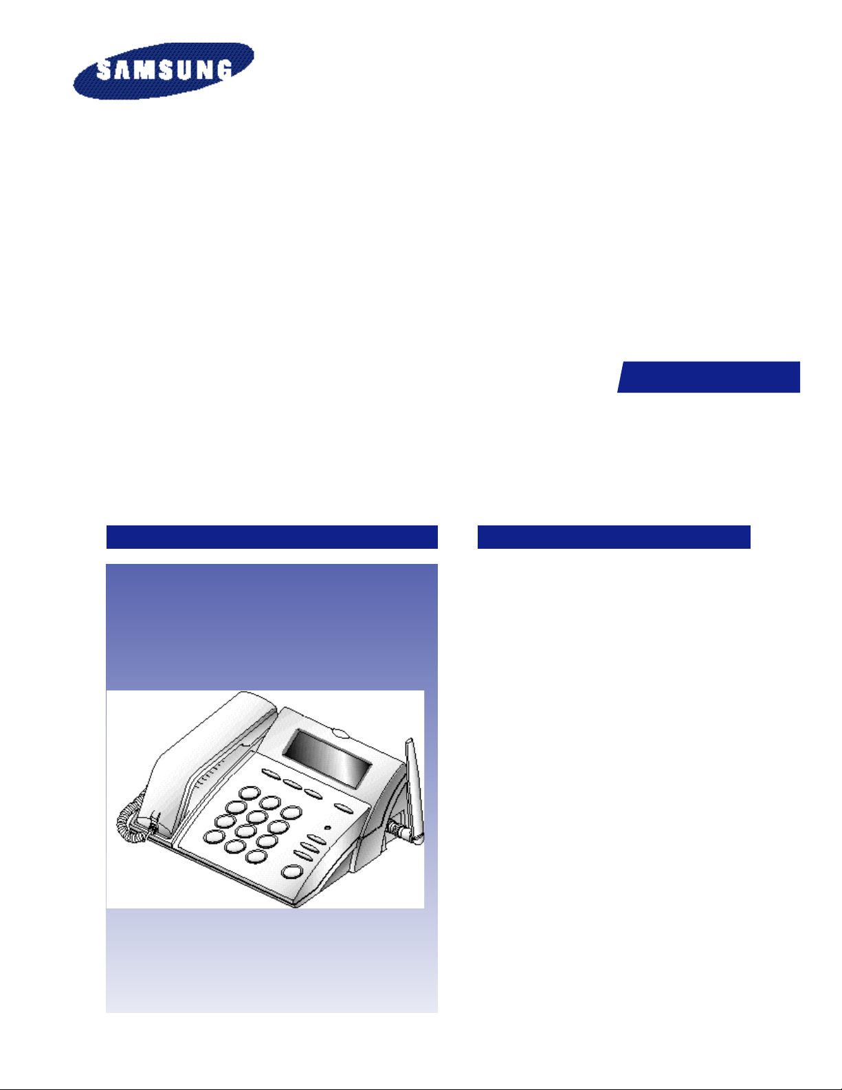
FIXED WIRELESS PHONE
Manual
SCW-F200
S E RVICE
FIXED WIRELESS PHONE
CONTENTS
1. Specification
2. NAM Programming
3. Data Transfer
4. Setup Method
5. Circuit Description
6. Troubleshooting
7. Exploded Views and Parts List
8. PCB Diagrams
9. Electrical Parts List
10. Block & Circuit Diagrams

Samsung Electronics Co.,Ltd.
GH68-60683A

2. NAM Programming
2.1 Switching the NAM(Numeric Assignment Module) writing mode
If you performs NAM writing mode, you have to enter the password, '4, 7, *, 8, 6, 9, #, 0, 8, #, 9'.
Keypads using in NAM writing mode are as follows :
0~9 : numberic keys
, # : Use to specify the variable which include several value.
VOLUME KEY : Use to switch the next item
CLR : Use to retouch a wrong digit
HOOK ON : Use to end a NAM writing mode
STO : Use to store data and switching the next function
RCL : Use to swich the last menu
Caution
-If you enter the NAM progrm mode, the last data displays on screen . When you need not change the
data, press VOLUME key to go to the next item.
-You can modify the data by entering a new data. And if you enter a wrong digit, press CLR to delete the
last digit.
-If you enter a wrong digit in the middle of NAM entering, continue to enter the next digits. After that
check and modify the data using volume key.
- While you check the data using volume, you can store the data by pressing STO key.
- When you enter the NAM, as there are necessary information enter the phone number and LOCK code
and press STO key.
When you enter NAM programming, display following three items.
1 GENERAL ; Display the variable used commonly NAM.
2 Setup NAM ; Display the variable of CDMA used commonly when you select NAM.
If you don't store the data by pressing STO key after modifying as explains, the data does not change.
You can check the data by pressing VOLUME key without changing the data.
Samsung Electronics 2-1

NAM Programming
2-2 Explaination about each item
2-2-1 GENERAL
When swiching the next item, press volume or STO key. (When you press STO key, store entered data.)
ESN ( Electronic serial number) : In Service Program, current ESN cannot be modifyed and entered but
displayed. If you want to modify ESN, special ESN Write Program is
needed. For more details, refer to 'ESN Writer manual'
CAI version (common Air Interface version) : The version of the Common Air Interface supported by the
mobile. Default setting is 2, CAI Version is not reset by user.
SCM (Station Class Mark) : Station Class Mark(SCM) displays the power class, transmission, slotted, dual
mode. SCM is not reset by user.
Lock Code : Default lock cord is 0000. It can be entered from 0000 to 9999.
SLOT Mode : Determine the slot mode of the mobile (using Yes-slot mode)
When changing ‘YES’ or ‘NO’, press or #.
Slot Index : Determine the solt mode index on slot mode the mobile.
The extent of index is from 0 to 9. The bigger the index of set, the longer sleeping time. The
sleeping time is longer the more power is saved. Default setting is 2.
2-2 Samsung Electronics

NAM Programming
2-2-2 Setup NAM
When you swich the next item, press volume or STO key. (If you press STO key, store the entered variable).
IMSI_MCC : Enter Mobile Country Code Default setting is 000.
IMSI_MNC : Enter Mobile Network Code Default setting is 00.
CDMA TEL NO : It is telephone number for CDMA
CDMA Pref : Select preferred system in using CDMA.
Home only, A only, A pref, B only, B pref.
CDMA ACCOLC : CDMA ACCESS OVERLOAD CLASS Default setting is 0.
Pchn Sys A : This is preferred system in using A system. OOO set 779, OOO set 0.
Pchn Sys B : This is preferred system in using B system. Default setting of OOO is 779 channel. Default
setting of OOO is 486 channel.
Schn Sys A : This is the second preferred system in using A system. OOO set 738, OOO set 0.
Schn Sys B : This is the second preferred system in using B system. Default setting of OOO is 738 channel.
Default setting of OOO is 568 channel.
CD Acq SID 1~CD Acq SID 6 : CDMA Acquisition SID. Enables you to set up to six SIDs. Default setting is
0, ranges from 0 to 32,767.
CD lock SID 1~CD lock SID 6 : CDMA lock SID
Enables you to set up to six SIDs.
Default setting is 0, ranges from 0 to 32767
CDMA Home SID : CDMA home SID Default setting is 'YES'.
Specify the Autonomous requisition in the home system.
SID #1 : (SID,NID) This is the first SID in using list.
NID #1 : (SID,NID) This is the first NID in using list.
SID #2 : (SID,NID) This is the second SID in using list.
NID #2 : (SID,NID) This is the second NID in using list.
SID #3 : (SID,NID) This is the third SID in using list
SID #3 : (SID,NID) This is the third NID in using list
SID #4 : (SID,NID) This is the fourth SID in using list
SID #4 : (SID,NID) This is the fourth NID in using list
SID #5 : (SID,NID) This is the fifth SID in using list
SID #5 : (SID,NID) This is the fifth NID in using list
Samsung Electronics 2-3

NAM Programming
The mobile determines the roaming status.
SID, NID list of OOOO and OOO is follingxzd
OOO : (2222, 1) (2222, 2) (2222, 3) (2222, 15) (0, 0)
OOO : (1700, 1) (1700, 2) 1700, 3) (1700, 15) (0, 0)
2-4 Samsung Electronics
2-3 Setting Up NAM
LCD Display Key in Function
NAM Programming
47*809#08#9
NAM Program
1:General
2:Setup NAM
ESN
B00000000
CAI version
SCM
01101010
Lock Code
0000
47 869#08#9 -selects NAM programming
1 -choose 'GENERAL.'
Volume Electronic Serial Number of the phone.
Volume
2
The version of the Common Air Interface supported by the mobile.
Volume Station Class Mark displays the power class (bit 0~1),
transmission (bit2), slotted (bit5), dual mode (bit6).
(0000)
4-digit code Four-digit number supplied by the user which enables
STO electronic locking of the phone.
Slot Mode
Yes
Slot Index
Pref NAM...
Digital pref
or Enables slot mode.
STO
0 - 7 Slot mode index.
2
STO Specifies the duration and frequency of times that the mobile
checks the paging channel. The higher the value, the less often the
mobile looks at the paging channel, and the more power is saved.
or Preferred system selection for NAM.
STO Up to four NAMs are allowed for the phone. This lists one of the
four NAMs and allows you to program both the FM and CDMA
settings.
Samsung Electronics 2-5

NAM Programming
LCD Display Key in Function
IMSI MCC
000
IMSI MNC
00
CDMA TEL NO.
987654321
CDMA pref...
B only
CDMA ACCOLC
Pchn Sys A
Pchn Sys B
486
Pchn Sys A
number International Mobile Station Identity Mobile Country Code.
STO
number International Mobile Station Identity Mobile Network Code.
STO
phone number CDMA phone number.
STO
or Preferred system selection.
STO
class number CDMA Access Overload Class.
0
STO This two-digit number specifies the level of priority assigned
to the mobile for accessing the system.
Ranges from 0 to 15.
channel number Primary CDMA channel for the A carrier.
0
STO Ranges from 0 to 1,023. 0 indicates no channel.
channel number Primary CDMA channel for the B carrier.
STO Ranges from 0 to 1,023. 0 indicates no channel.
channel number Secondary CDMA channel for the A carrier.
0
STO Suggested setting is 0: ranges from 0 to 1,023.
Schn Sys B
568
CD Acq SID (1-6)
0
CD lockSID (1-6)
0
CDMA HomeSID
Yes
channel number Secondary CDMA channel for the B carrier.
STO Suggested setting is 0: ranges from 0 to 1,023.
ID number CDMA Acquisition System ID.
STO Enables you to set the phone to acquire up to six SIDs in the
CDMA mode. If you enter ‘0’ for any SID, the program
assumes that you have no more numbers to store.
Default setting is 0: ranges from 0 to 32,767: up to six SIDs.
ID number CDMA Lock System ID.
STO Enable you to specify up to six SIDs that the phone will be
prohibited from acquiring in CDMA mode. If all six SIDs are
set to zero, no lock restrictions will be in effect and the phone
can acquire all SIDs.
Default setting is 0: ranges from 0 to 32,767 up to six SIDs.
or CDMA Home System ID.
STO Enables the phone to allow mobile terminated calls while in
the home system. Controls the types of registration allowed for
the phone.
2-6 Samsung Electronics

LCD Display Key in Function
NAM Programming
CDMA fSID
CDMA fNID
SID #1
NID #1
Yes
Yes
1700
or CDMA foreign System ID.
STO Enables the phone to allow mobile terminated calls while
in a foreign system. Controls the types of registration
allowed for the phone.
or CDMA foreign Network ID.
STO Enables the phone to allow mobile terminated calls while
in a foreign system and foreign network ID. Controls the
types of registration allowed for the phone.
number System Identification Number.
STO Controls how the phone acquires different systems.
Determines the roaming status for the mobile.
All SIDs range from 0 to 32,767: a 0 setting for the SID
signifies that it is not active.
number Network Identification Number.
1
STO Controls how the phone acquires different systems, and is
set and specified in conjunction with each SID (e.g., SID #1,
NID #1).
Determines the roaming status for the mobile.
All SIDs range from 0 to 65,535: a 0 setting for one NID
signifies that it is not active.
SID #2
SID #2
SID #2
NID #3
SID #4
NID #4
SID #5
1700
1700
1700
3
1700
15
0
number See SID #1.
STO
number See NID #1.
STO
number See SID #1.
STO
number See NID #1.
STO
number See SID #1.
STO
number See NID #1.
STO
number See SID #1.
STO
NID #5
0
number See NID #1.
STO
Samsung Electronics 2-7

NAM Programming
2-8 Samsung Electronics
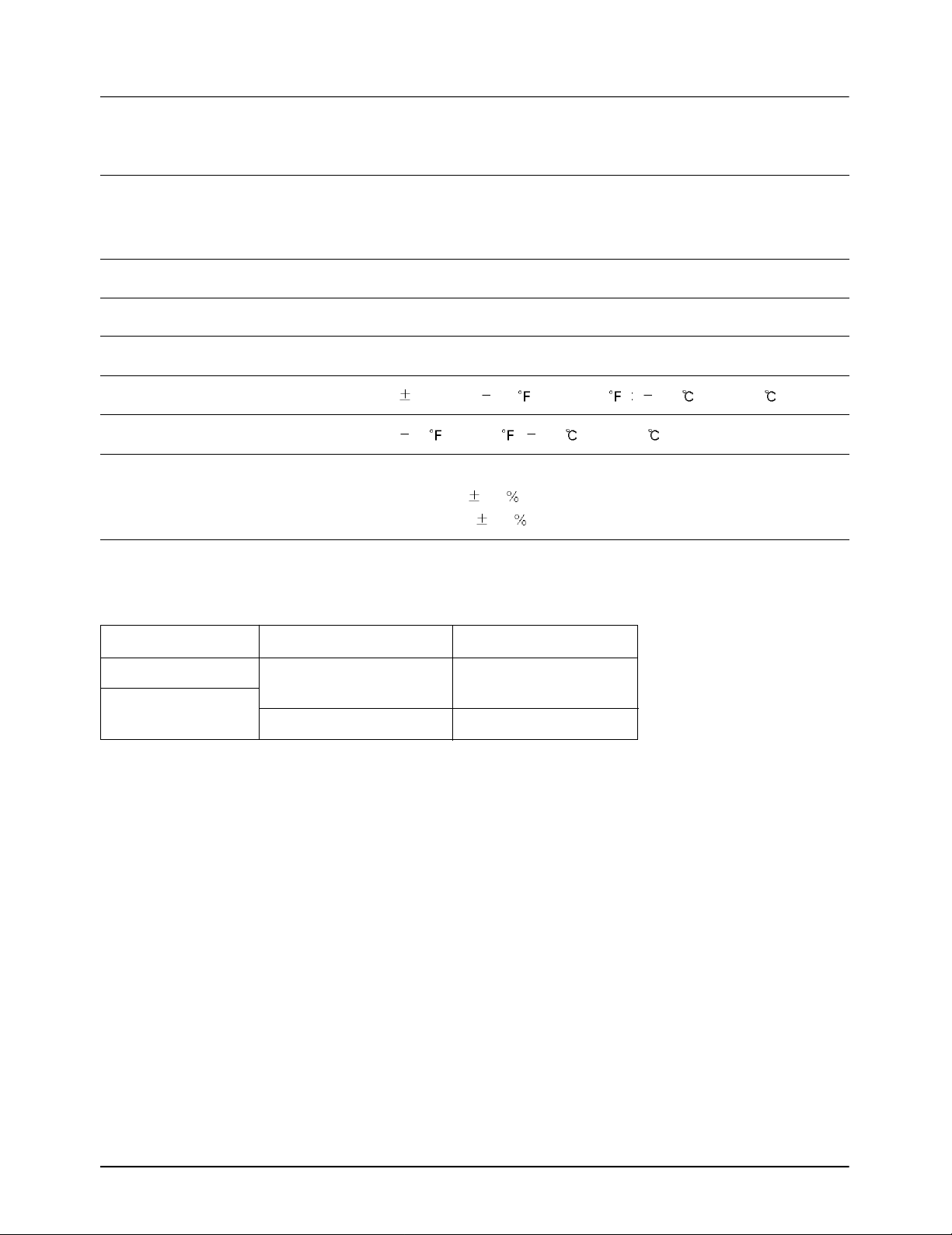
£´140 30 ~ £´60 )
Operating Temperature : 4 ~ 122 ( 20 ~ £´50 )
Operating Voltage
Battery : 5.0V DC ( 10 )
Adapter : 11.0V DC ( 20 )
Size and Weight
w/ battery :218 °ø210 °ø73 mm 1183 gr
Samsung Electronics 1-1
1. Specification
Operating Time
Digital mode
Standby Time
51~ 75 hours
(slot index 2)
Talk Time
6 hours
w/ battery
1-1 General
Frequency Range Digital Mode
Transmitter : 824.64 ~ 848.37 MHz
Receiver : 869.64 ~ 893.37 MHz
Channel Spacing : 1.23 MHz 30 kHz
Number of Channels : 20 FA 832 CHs
Duplex Spacing : 45 MHz
Frequency Stability : 2.5 ppm ( 22 ~
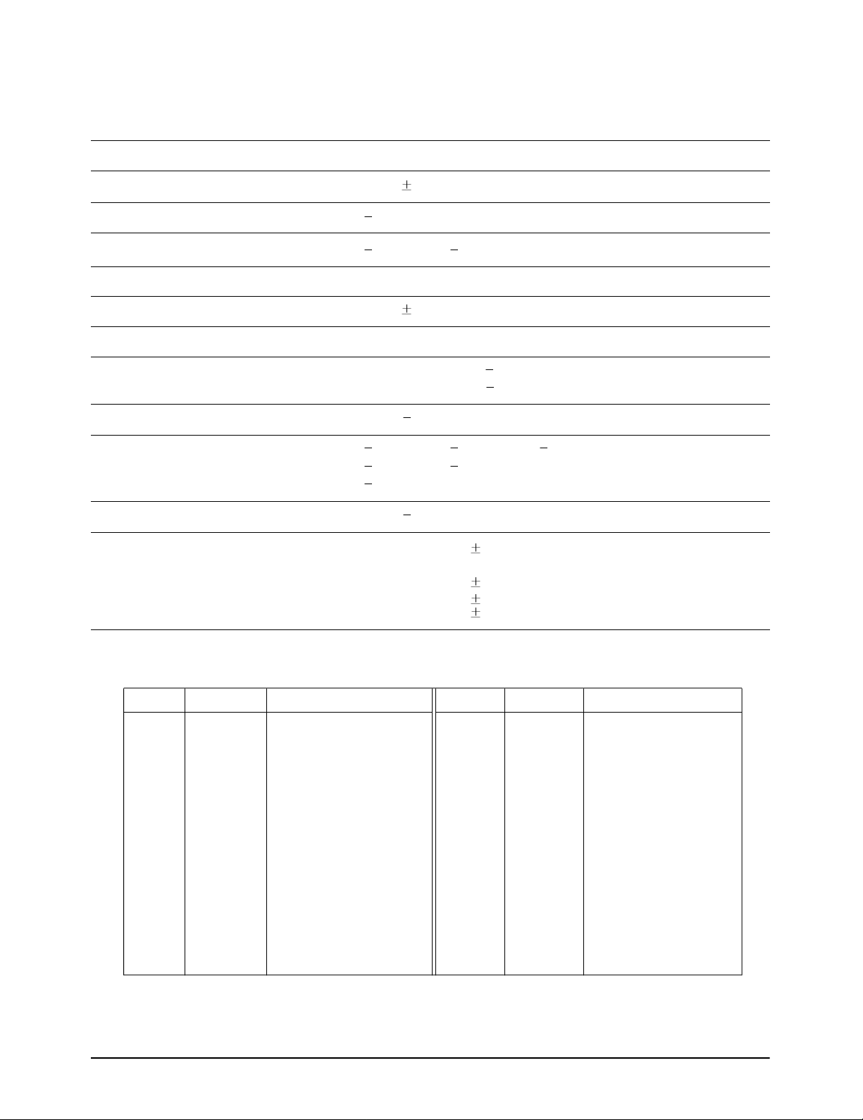
Specification
£´1.5 dBm
104 dBm : £´18.0 dBm ~ £´30.0 dBm
Standby Output Power : below 61 dBm
Closed Loop TX Power Control Range : Test 1 beyond 24 dB
Test 2 0 mS ~ 2.5 mS
Test 3 beyond 24 dB
Test 4 beyond 24 dB
Test 5 beyond 24 dB
MSC Transmitter Frequency
FA NO. CH. NO. CENTER FREQUENCY FA NO. CH. NO. CENTER FREQUENCY
1 1011 824.640MHz 11 404 837.120MHz
2 29 825.870MHz 12 445 838.350MHz
3 70 827.100MHz 13 486 839.580MHz
4 111 828.330MHz 14 527 840.810MHz
5 152 829.560MHz 15 568 842.040MHz
6 193 830.790MHz 16 609 843.270MHz
7 234 832.020MHz 17 650 844.270MHz
8 275 833.250MHz 18 697 845.910MHz
9 316 834.480MHz 19 738 847.140MHz
10 363 835.890MHz 20 779 848.370MHz
1-2 Digital Mode
Waveform Quality : above 0.944
Time Reference : within 1uS
RX Sensitivity : 104 dBm, FER = within 0.5%
Dynamic Range : 104 dBm ~ 25 dBm, FER = within 0.5%
TX Output Power : Maximum 320 mW (25dBm)
TX Frequency Deviation : within 300 Hz
Occupied Band Width : 1.32 MHz
TX Conducted Spurious Emissions : 900 kHz below 42 dBc / 30 kHz
: 1.98 MHz below 54 dBc / 30 kHz
Minimum TX Power Control : below 50 dBm
Open Loop Power Control : 25 dBm : 57.0 dBm ~ 38.5 dBm
65 dBm : 17.5 dBm ~
1-2 Samsung Electronics

MSC Receiver Frequency
FA NO. CH. NO. CENTER FREQUENCY FA NO. CH. NO. CENTER FREQUENCY
1 1011 869.640MHz 11 404 882.120MHz
2 29 870.870MHz 12 445 883.350MHz
3 70 872.100MHz 13 486 884.580MHz
4 111 873.330MHz 14 527 885.810MHz
5 152 874.560MHz 15 568 887.040MHz
6 193 875.790MHz 16 609 888.270MHz
7 234 877.020MHz 17 650 889.270MHz
8 275 878.250MHz 18 697 890.910MHz
9 316 879.480MHz 19 738 892.140MHz
10 363 880.890MHz 20 779 893.370MHz
Specification
Samsung Electronics 1-3

Specification
1-4
Samsung Electronics

4. Setup Method
Samsung Electronics 4-1

Operating Instruction
4-2 Samsung Electronics

6. Circuit Description
6-1 Logic Section
6-1-1 Power Supply
With the battery installed on the phone and by
pressing the PWR key, the VBATT and ON_SW
signals will be connected. This will turn on Q102
(2SC4081BR) and will drive DC-DC converter
(U123) to output 5.0V. This in turn will be
supplied to pin 6 of regulators (U121 and U122),
thus releasing them from the shut-down state to
output regulated 3.3V.
The VBATT applied to ON_SW will turn on Q103
(DTC144EE) resulting in the signal
ON_SW_SENSE to change state from HIGH to
LOW. This will allow MSM to send out PS_HOLD
(logical HIGH) to turn on Q102 even after the
PWR key is released.
The voltage (+3.3V) from U121 is used in the
digital parts of MSM and BBA. The voltage
(+3.3AV) from U122 is used in the analog part of
BBA. The voltage from U124 (output of 5V) is used
for the audio circuitry.
6-1-2 Logic Part
The Logic part consists of internal CPU of MSM,
RAM, ROM and EEPROM. The MSM receives
TCXO and CHIPX8 clock signals from the BBA
and controls the phone during the CDMA and the
FM mode. The major components are as follows:
CPU : INTEL 80186 core
FROM : U126 (MBM29LV800T) - 8MBIT
FLASH ROM
SRAM : U127 (KM68V2000I) - 2MBIT
STATIC RAM
EEPROM : U113 (AT24C128) - 128KBIT SERIAL
EEPROM
CPU
INTEL 80186 CMOS type 16-bit microprocessor is
used for the main processing. The CPU controls all
the circuitry. For the CPU clock, 27MHz resonator
is used.
FLASH ROM
One 8 MBIT FROM is used to store the terminal's
program. Using the down-loading program, the
program can be changed even after the terminal is
fully assembled.
SRAM
One 2 MBIT SRAM is used to store the internal
flag information, call processing data, and timer
data.
EEPROM
One 128 KBIT EEPROM is used to store ESN,
NAM, power level, volume level, and telephone
number.
KEYPAD
For key recognition, key matrix is setup using
SCAN0-6 of STORE signals and KEY0-3 of input
ports of MSM. Eight LEDs and backlight circuitry
are included in the keypad for easy operation in
the dark.
LCD MODULE
LCD module contains a controller which will
display the information onto the LCD by 8-bit data
from the MSM. It also consists a DC-DC converter
to supply -3.5V for fine view angle and LCD
reflector to improve the display efficiency.
Samsung Electronics - Contents may change without notice. 6-1

Circuit Description
6-1-3 Baseband Part
MOBILE SYSTEM MODEM (MSM)
The MSM equipped with the INTEL 80186 CPU
core is an important component of the CDMA
cellular phone. The MSM comes in a 176 pins
TQFP package. The interface block diagram is
shown on page 6-3.
MICROPROCESSOR INTERFACE
The interface circuitry consists of reset circuit,
address bus (A0-A19), data bus (AD0-AD15), and
memory controls (ALE, DT_R, HWR/, LWR/,
RAM_CS/, ROM_CS).
INPUT CLOCK
CPU clock: 27 MHz
TXCO/4 (pin 34): 4.92 MHz. This clock signal
from the BBA is the reference clock for the MSM
except in CDMA mode.
CHIPX8 : 9.8304 MHz. The reference clock used
during the CDMA mode.
ADC Interface
ADC_CLK (pin 3), ADC_ENABLE (pin 1) and
ADC_DATA (pin 2) are required to control the
internal ADC in the BBA.
Data Port Interface
Includes the UART. Also, supports Diagnostic
Monitor (DM) and HP equipment interface.
CODEC Interface
The MSM outputs 2.048 MHz PCM_CLK (pin 19)
and 8 KHz CODEC_SYNC (pins 16,20) to the
CODEC (U117). The voice PCM data from the
MSM (U101) PCM_DIN (pin135) is compressed
into 8KHz by QCELP algorithm in the CDMA
mode. In FM mode, the data is processed by
D_FM.
RF Interface
BBA INTERFACE
CDMA, FM Data Interface
TXIQDATA0-7 (pins 24-32) : TX data bus used
during both CDMA and FM mode.
C_RX_IDATA0-3 (pins 16-20) and
C_RX_QDATA0-3 (pins 12-15) : RX data bus
used during CDMA mode.
FM_RX_IDATA (pin 7) and FM_RX_QDATA
(pin 8) : RX data bus used during FM mode.
Clock
TX_CLK (pin 22), TX_CLK/(pin 23) : Analog to
Digital Converter (ADC) reference clock used in
TX mode.
CHIPX8 : ADC reference clock used in CDMA
RX mode.
FMCLK : Reference clock in FM RX mode.
TX : TX_AGC_ADJ (pin 35) port is used to control
the TX power level and PA_ON (pin 44) signal is
used to control the power amplifier.
RX : AGC_REF (pin 36) port is used to control the
RX gain and TRK_LO_ADJ (pin 45) is used to
compensate the TCXO clock.
General Purpose I/O Register Pins
Input/output ports to control external devices.
Power Down Control
When the IDLE/ signal turns LOW, only the TX
sections will be disabled. If both the IDLE/ and
SLEEP/ changes to LOW, all the pins except for
the TXCO is disabled.
6-2 Samsung Electronics - Contents may change without notice.

Circuit Description
Figure 6-1 Baseband Block Diagram
Samsung Electronics - Contents may change without notice. 6-3

Circuit Description
6-1-4 Audio Part
TX AUDIO PATH
The voice signal output from microphone is
filtered and amplified by the internal OP-AMP
and is converted to PCM data by the CODEC
(U117). This signal is then applied to the MSM
(U101)'s internal vocoder.
RX AUDIO PATH
The PCM data out from the MSM is converted to
audio signal by ADC of CODEC (U117), is then
amplified by the speaker amplifier (U111) to be
sent to the speaker unit.
FM TX PATH
Pre-Emphasis Circuit
The circuit features +6dB/oct to reduce signal loss
and noise in Tx path.
Compressor
RX AUDIO PATH
De-Emphasis Circuit
This circuit is 1st LPF featuring -6dB/oct to reduce
signal loss and noise in Rx path.
Expander
The expander features 1:2 level to reduce signal
loss and noise in Rx path. The zero crossing level
of the expander is 2.9 kHz/dev, attack time is 3
mS, and release time is 13.5 mS.
Volume Adjust
Volume can be adjusted up to 4 steps for the user
to obtain a proper loudness of received signal.
6-1-5 TX WBD, ST, And SAT
These signals are generated from MSM. The
modulation level of TX WBD and ST is
8kHz/dev, and SAT is 2kHz/dev.
The compressor features 2:1 level to reduce signal
loss and noise in Tx path. The zero crossing level
of the compressor is 2.9 kHz/dev, attack time is
3 mS, and release time is 13.5 mS.
Limiter
The limiter performs to cut 0.53 Vp-p or higher
audio signal level so that the FM frequency
deviation is not over 12kHz/dev. The function
is used to avoid confusion over phone line. LPF is
used to reduce a specific high frequency of limited
signal.
6-1-6 Buzzer Driving Circuitry
Buzzer generates alert tone. When the buzzer
receives the timer signal from the MSM, it
generates alert tone. The buzzer level is adjusted
by the alert signal's period generated from the
MSM timer.
6-1-7 Key Tone Generator
Ringer signal (pin 49) out from MSM (U101) is
passed through 2 serial LPF consisting of R141,
C145, R145, and C142, amplified at the speaker
amp (U111), and comes out to speaker. In handsfree mode, the key tone is applied to RX audio line
through the LPF and C153, R142.
6-4 Samsung Electronics - Contents may change without notice.

6-2 Receiver Section
Circuit Description
LOW NOISE AMPLIFIER (LNA)
The low noise amplifier featuring 1.5dB and 16 dB
gain amplifies a weak signal received from the
base station to obtain the optimum signal level.
DOWN CONVERTER (MIXER)
First local signal is applied to this down converter.
The down converter transfers the signal amplified
at the LNA into 85.38 MHz IF signal. 85 MHz IF
signal is made by subtracting 881 12.5 MHz RF
signal from 966 12.5MHz first local signal.
RX IF AUTOMATIC GAIN CONTROLLER
(AGC) AMP
85.38 MHz IF signal is applied to IF AGC amp, the
IF AGC output level is applied to BBA (Baseband
Analog ASIC). The IF AGC amp (U302) keep the
signal at a constant level by controlling the gain.
Dynamic range is 90 dB, up gain +45dB, and down
gain -45dB.
IF SAW BAND PASS FILTER FOR CDMA
IF SAW BPF (F303) is used for CDMA system
having 1.23 MHz wide band and 630 kHz band
width. The filter also eliminates the image product
generated at the mixer.
BUFFER
Buffer (Q342) amplifies signal to be applied to the
local input of the down converter (U301) when a
phase is locked between VCO (U341) and PLL IC
(U342).
VOLTAGE CONTROLLED OSCILLATOR
The VCO (U341) generates the signal having 966
MHz center frequency and 12.5 MHz deviation
with the voltage control. PLL IC (U342) controls
this signal.
PHASE LOCKED LOOP (PLL)
RF BAND PASS FILTER (BPF)
The RF BPF (F302) accepts only a specific
frequency (881 12.5MHz) from the signal
received from the mobile station. The band width
is 25 MHz.
IF SAW BAND PASS FILTER FOR AMPS
IF SAW BPF (F304) is used for AMPS system
having 30 kHz channel spacing and 15 kHz
band width. The filter also eliminates the image
product generated at the mixer.
Input reference frequency is generated at
VC_TCXO (U343) and the divided signal is
generated at VCO (U341). PLL compares the two
signals and generates the desired signal with a
pre-programmed counter which controls voltage.
VOLTAGE CONTROLLED TEMPERATURE
COMPENSATED CRYSTAL OSCILLATOR
It provides 19.68 MHz reference frequency to the
mobile main set. A correct frequency tuning is
made by the voltage control.
THERMISTOR
The thermistor (U371) detects temperature. It is
used to compensate active component
characteristics due to the temperature difference.
Samsung Electronics - Contents may change without notice. 6-5

Circuit Description
DUPLEXER
Duplexer (F301) controls to transmit through the
antenna only the signals within acceptable Tx
frequency range (836 12.5 MHz) and to receive
through the antenna only the signals within
acceptable Rx frequency range (881 12.5 MHz).
It also matches LNA (U301) input in receiving part
and PA output in transmitter part with the
antenna.
6-3 Transmitter Section
BASEBAND ANALOG ASIC (BBA)
BBA (U401) consists of ADC, DAC, LPF
(FM/CDMA), divider, VCO, logic control circuit,
PLL, and mixer.
BBA performs a specific function between RF part
and logic part, with MSM. The IF signal out from
Rx IF AGC amp is secondly converted through the
down-converter. The signal passes through the
CDMA or FM filter, converts to digital signal
through ADC, then is sent to MSM. The digital
signal out from MSM converts to analog signal
through DAC. The analog signal converts to the IF
signal through each filter and the up-converter.
POWER SUPPLY REGULATOR
The power supply regulator (U381, U382)
generates a regulated power (3.6VR).
ANTENNA
Antenna (ANT1) allows signals to send to receive
from the base station.
IF AUTOMATIC GAIN CONTROLLER AMP
The signal out to the base station should be a
constant level. The TX IF AGC amp (U460)
controls power to keep the signal at a constant
level. Dynamic range is 85 dB, up gain +40dB, and
down gain -45dB.
RF BAND PASS FILTER (BPF)
The RF BPF (F451) accepts only a specific
frequency (836 12.5MHz) to send it out to the
base station. The band width is 25 MHz.
POWER SUPPLY SWITCHING
POWER AMP MODULE
Power supply switching (Q483) turns on
Power Amp module (U467) amplifies signal (28 dB
Gain) to be sent out to the base station through the
antenna .
TX_POWER when the phone is in traffic mode and
supplies power to the circuits.
ISOLATOR
UP CONVERTER (MIXER)
The up-converter (U461) receives the first local
signal to generate 836 12.5 MHz from the signal
controlled by TX IF AGC amp (U460). 836 12.5
MHz signal comes out from the mixer output by
subtracting 130 MHz IF signal from 966 12.5
MHz first local signal. The driver amp and this upconverter are packaged into one in U461.
6-6 Samsung Electronics - Contents may change without notice.
Isolator (U468) is used to reduce a reflected signal
to protect the power amp module from being
damaged.
POWER SUPPLY REGULATOR
The power supply regulator (U482, U483) supply a
regulated power to each part of transmitter. U483
supplies 4.7V to TX mixer (U461) and OP amp
(U463). U482 supplies 3.6 V to TX IF AGC amp
(U460).

6-4 Rapid Desk-Top Charger
Rapid Charger, DTC58 is composed of power supply part and control part.
Circuit Description
6-4-1 Power Supply Part (Flyback type
SMPS circuit)
AC INPUT
AC input protection circuit and rectifier circuit
AC power through the AC plug is rectifiered to
DC power of high voltage through the BD1 and
C2. MOV1 is used by protection circuit from AC
power surge. F1 is fuse to prevent over current. C1
and LF1 is EMI noise protection filter of switching
power.
Switching controller and transformer
IC1 supplies constant voltage and constant current
to secondary circuit through the transformer. D1,
D2 absorbs the reverse voltage when transformer
winding turns off.
SECONDARY POWER
Secondary DC/DC converter circuit : Q2, D8, L3,
C19
It changes the DC output voltage to 8.4V through
step-down chopper method.
Reverse current protection circuit : D6, D7
When power is off, it protects the reverse flow of
current from battery pack.
6-4-2 Control Part
MICOM CONTROLLER : HIC
HIC is include u-COM to controlled whole
charging system and include following internal
circuit :
-General Input/Output port
-A/D converter
-Reset delay circuit (Power on delay)
-Timer
Output constant voltage circuit : HIC, IC7, VR1
The HIC detects output voltage and compares it
with reference voltage in HIC. The error is FED to
primary circuit by IC7A. The feeback error is
converted to current by IC7B and D3. The current
controlls IC1.
It is carried following functions :
-Battery Recognition
-Charging termination condition detection
-Output short detection and output protection
-Temperature detection
BATTERY RECOGNITION CIRCUIT : HIC
Secondary rectifier circuit : D4, D5, C8, C11
The secondary AC output of transformor is
rectified to DC voltage.
Secondary filter circuit : L1, L2, C9, C12
It minimizes the high frequency ripple noise,
which is caused by primary oscilation.
Samsung Electronics - Contents may change without notice. 6-7
Battery identity detection determined to voltage
detection battery internal between C/F and GND.

Circuit Description
CURRENT DETECTION CIRCUIT : R5, R6,
R11, R12, HIC
Battery charging current is changed voltage
through R5, R6, R11, R12. This voltage inputed
u-COM to 16 times amplifiered through HIC.
VOLTAGE DETECTION CIRCUIT : HIC
u-COM A/D through HIC pin 12, 13 detected
voltage.
6-5 Hands-Free Kit
6-5-1 Charging Circuit
BATTERY TEMPERATURE DETECTION
CIRCUIT : HIC, TH1
Battery temperature detection determined
temperature by ues of thermistor registor variation
of THI by HIC.
CURRENT LIMIT CIRCUIT : HIC
When soft-change, current detection circuit
limited current flow to battery, reference voltage
more than detected current, detected current and
HIC internal reference voltage.
6-5-3 Speaker circuit
A constant voltage is used for the hands-free kit.
This circuit converts DC 12V input current to 8.4V
DC to charge the battery. When the battery is fully
charged, the charge current drops and the circuit
operates as a constant voltage.
6-5-2 u-Processor
Micro processor controls charging power and
charging current to protect the phone. It also
allows to communicate with a HHP, and to
convert from hands-free mode to private mode,
and vice verse. It adjusts speaker volume at 8 steps
and attenuates echo and noise occurred during
conversation.
This circuit eliminates HHP noise, and controls
the sound quality and speaker volume using
analog C-mos IC which checks the speaker signal
up to 8 steps. 5W audio amplifier amplifies the
speaker signal.
6-5-4 Microphone Circuit
This circuit separates ground to eliminate the
noise occurring from the HHP antenna and
microphone. u-processor controls this circuit to
attenuate echo which may occur in Land side.
6-8 Samsung Electronics - Contents may change without notice.
 Loading...