


6. Circuit Description
6-1 Logic Section
6-1-1 Power Supply
With the battery installed on the phone and by
pressing the PWR key, the VBATT and ON_SW
signals will be connected. This will turn on Q102
(2SC4081BR) and will drive DC-DC converter
(U123) to output 5.0V. This in turn will be
supplied to pin 6 of regulators (U121 and U122),
thus releasing them from the shut-down state to
output regulated 3.3V.
The VBATT applied to ON_SW will turn on Q103
(DTC144EE) resulting in the signal
ON_SW_SENSE to change state from HIGH to
LOW. This will allow MSM to send out PS_HOLD
(logical HIGH) to turn on Q102 even after the
PWR key is released.
The voltage (+3.3V) from U121 is used in the
digital parts of MSM and BBA. The voltage
(+3.3AV) from U122 is used in the analog part of
BBA. The voltage from U124 (output of 5V) is used
for the audio circuitry.
6-1-2 Logic Part
The Logic part consists of internal CPU of MSM,
RAM, ROM and EEPROM. The MSM receives
TCXO and CHIPX8 clock signals from the BBA
and controls the phone during the CDMA and the
FM mode. The major components are as follows:
CPU : INTEL 80186 core
FROM : U126 (MBM29LV800T) - 8MBIT
FLASH ROM
SRAM : U127 (KM68V2000I) - 2MBIT
STATIC RAM
EEPROM : U113 (AT24C128) - 128KBIT SERIAL
EEPROM
CPU
INTEL 80186 CMOS type 16-bit microprocessor is
used for the main processing. The CPU controls all
the circuitry. For the CPU clock, 27MHz resonator
is used.
FLASH ROM
One 8 MBIT FROM is used to store the terminal's
program. Using the down-loading program, the
program can be changed even after the terminal is
fully assembled.
SRAM
One 2 MBIT SRAM is used to store the internal
flag information, call processing data, and timer
data.
EEPROM
One 128 KBIT EEPROM is used to store ESN,
NAM, power level, volume level, and telephone
number.
KEYPAD
For key recognition, key matrix is setup using
SCAN0-6 of STORE signals and KEY0-3 of input
ports of MSM. Eight LEDs and backlight circuitry
are included in the keypad for easy operation in
the dark.
LCD MODULE
LCD module contains a controller which will
display the information onto the LCD by 8-bit data
from the MSM. It also consists a DC-DC converter
to supply -3.5V for fine view angle and LCD
reflector to improve the display efficiency.
Samsung Electronics - Contents may change without notice. 6-1

Circuit Description
6-1-3 Baseband Part
MOBILE SYSTEM MODEM (MSM)
The MSM equipped with the INTEL 80186 CPU
core is an important component of the CDMA
cellular phone. The MSM comes in a 176 pins
TQFP package. The interface block diagram is
shown on page 6-3.
MICROPROCESSOR INTERFACE
The interface circuitry consists of reset circuit,
address bus (A0-A19), data bus (AD0-AD15), and
memory controls (ALE, DT_R, HWR/, LWR/,
RAM_CS/, ROM_CS).
INPUT CLOCK
CPU clock: 27 MHz
TXCO/4 (pin 34): 4.92 MHz. This clock signal
from the BBA is the reference clock for the MSM
except in CDMA mode.
CHIPX8 : 9.8304 MHz. The reference clock used
during the CDMA mode.
ADC Interface
ADC_CLK (pin 3), ADC_ENABLE (pin 1) and
ADC_DATA (pin 2) are required to control the
internal ADC in the BBA.
Data Port Interface
Includes the UART. Also, supports Diagnostic
Monitor (DM) and HP equipment interface.
CODEC Interface
The MSM outputs 2.048 MHz PCM_CLK (pin 19)
and 8 KHz CODEC_SYNC (pins 16,20) to the
CODEC (U117). The voice PCM data from the
MSM (U101) PCM_DIN (pin135) is compressed
into 8KHz by QCELP algorithm in the CDMA
mode. In FM mode, the data is processed by
D_FM.
RF Interface
BBA INTERFACE
CDMA, FM Data Interface
TXIQDATA0-7 (pins 24-32) : TX data bus used
during both CDMA and FM mode.
C_RX_IDATA0-3 (pins 16-20) and
C_RX_QDATA0-3 (pins 12-15) : RX data bus
used during CDMA mode.
FM_RX_IDATA (pin 7) and FM_RX_QDATA
(pin 8) : RX data bus used during FM mode.
Clock
TX_CLK (pin 22), TX_CLK/(pin 23) : Analog to
Digital Converter (ADC) reference clock used in
TX mode.
CHIPX8 : ADC reference clock used in CDMA
RX mode.
FMCLK : Reference clock in FM RX mode.
TX : TX_AGC_ADJ (pin 35) port is used to control
the TX power level and PA_ON (pin 44) signal is
used to control the power amplifier.
RX : AGC_REF (pin 36) port is used to control the
RX gain and TRK_LO_ADJ (pin 45) is used to
compensate the TCXO clock.
General Purpose I/O Register Pins
Input/output ports to control external devices.
Power Down Control
When the IDLE/ signal turns LOW, only the TX
sections will be disabled. If both the IDLE/ and
SLEEP/ changes to LOW, all the pins except for
the TXCO is disabled.
6-2 Samsung Electronics - Contents may change without notice.
Circuit Description
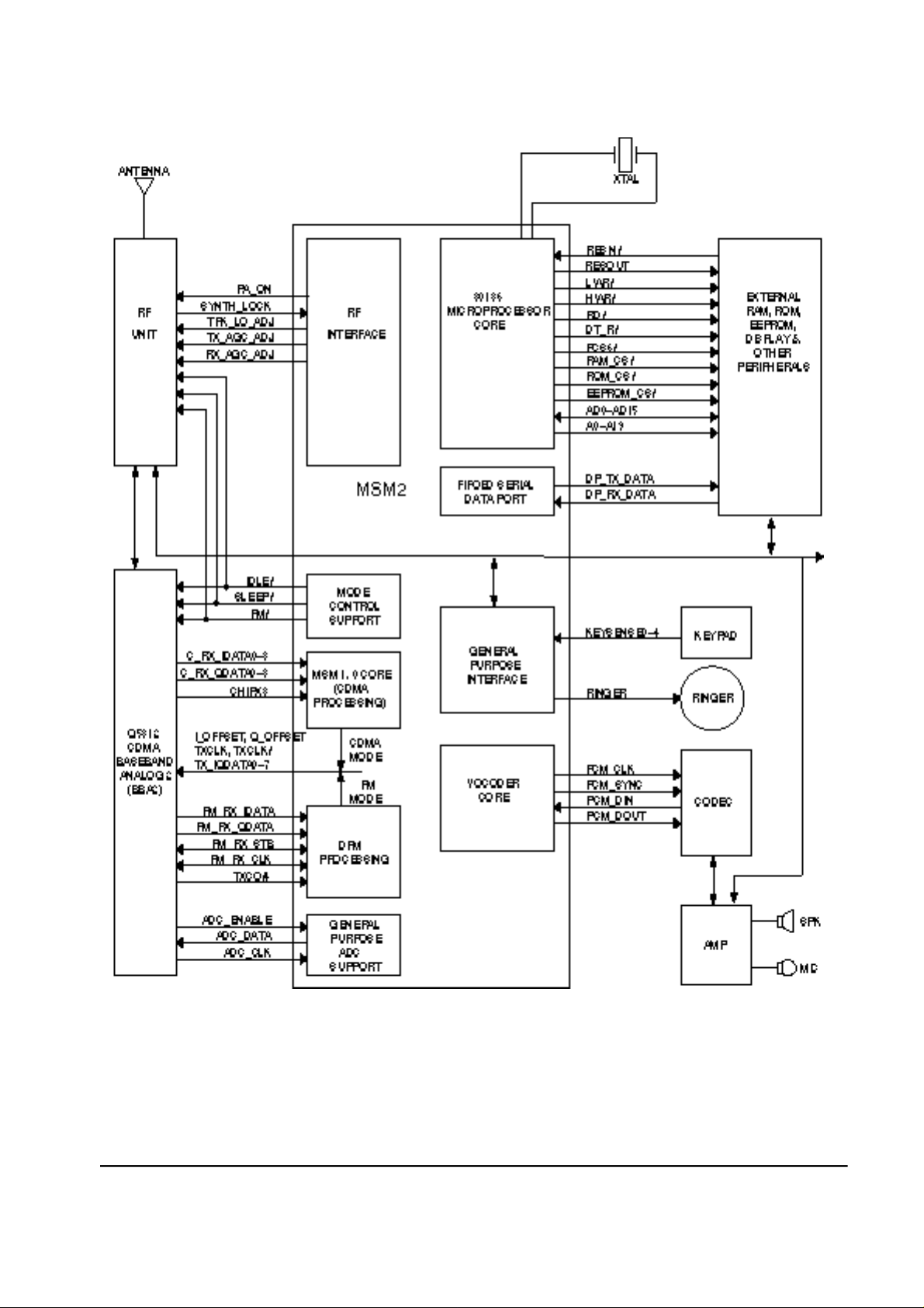
Figure 6-1 Baseband Block Diagram
Samsung Electronics - Contents may change without notice. 6-3

Circuit Description
6-1-4 Audio Part
TX AUDIO PATH
The voice signal output from microphone is
filtered and amplified by the internal OP-AMP
and is converted to PCM data by the CODEC
(U117). This signal is then applied to the MSM
(U101)'s internal vocoder.
RX AUDIO PATH
The PCM data out from the MSM is converted to
audio signal by ADC of CODEC (U117), is then
amplified by the speaker amplifier (U111) to be
sent to the speaker unit.
FM TX PATH
Pre-Emphasis Circuit
The circuit features +6dB/oct to reduce signal loss
and noise in Tx path.
Compressor
RX AUDIO PATH
De-Emphasis Circuit
This circuit is 1st LPF featuring -6dB/oct to reduce
signal loss and noise in Rx path.
Expander
The expander features 1:2 level to reduce signal
loss and noise in Rx path. The zero crossing level
of the expander is 2.9 kHz/dev, attack time is 3
mS, and release time is 13.5 mS.
Volume Adjust
Volume can be adjusted up to 4 steps for the user
to obtain a proper loudness of received signal.
6-1-5 TX WBD, ST, And SAT
These signals are generated from MSM. The
modulation level of TX WBD and ST is
8kHz/dev, and SAT is 2kHz/dev.
The compressor features 2:1 level to reduce signal
loss and noise in Tx path. The zero crossing level
of the compressor is 2.9 kHz/dev, attack time is
3 mS, and release time is 13.5 mS.
Limiter
The limiter performs to cut 0.53 Vp-p or higher
audio signal level so that the FM frequency
deviation is not over 12kHz/dev. The function
is used to avoid confusion over phone line. LPF is
used to reduce a specific high frequency of limited
signal.
6-1-6 Buzzer Driving Circuitry
Buzzer generates alert tone. When the buzzer
receives the timer signal from the MSM, it
generates alert tone. The buzzer level is adjusted
by the alert signal's period generated from the
MSM timer.
6-1-7 Key Tone Generator
Ringer signal (pin 49) out from MSM (U101) is
passed through 2 serial LPF consisting of R141,
C145, R145, and C142, amplified at the speaker
amp (U111), and comes out to speaker. In handsfree mode, the key tone is applied to RX audio line
through the LPF and C153, R142.
6-4 Samsung Electronics - Contents may change without notice.

6-2 Receiver Section
Circuit Description
LOW NOISE AMPLIFIER (LNA)
The low noise amplifier featuring 1.5dB and 16 dB
gain amplifies a weak signal received from the
base station to obtain the optimum signal level.
DOWN CONVERTER (MIXER)
First local signal is applied to this down converter.
The down converter transfers the signal amplified
at the LNA into 85.38 MHz IF signal. 85 MHz IF
signal is made by subtracting 881 12.5 MHz RF
signal from 966 12.5MHz first local signal.
RX IF AUTOMATIC GAIN CONTROLLER
(AGC) AMP
85.38 MHz IF signal is applied to IF AGC amp, the
IF AGC output level is applied to BBA (Baseband
Analog ASIC). The IF AGC amp (U302) keep the
signal at a constant level by controlling the gain.
Dynamic range is 90 dB, up gain +45dB, and down
gain -45dB.
IF SAW BAND PASS FILTER FOR CDMA
IF SAW BPF (F303) is used for CDMA system
having 1.23 MHz wide band and 630 kHz band
width. The filter also eliminates the image product
generated at the mixer.
BUFFER
Buffer (Q342) amplifies signal to be applied to the
local input of the down converter (U301) when a
phase is locked between VCO (U341) and PLL IC
(U342).
VOLTAGE CONTROLLED OSCILLATOR
The VCO (U341) generates the signal having 966
MHz center frequency and 12.5 MHz deviation
with the voltage control. PLL IC (U342) controls
this signal.
PHASE LOCKED LOOP (PLL)
RF BAND PASS FILTER (BPF)
The RF BPF (F302) accepts only a specific
frequency (881 12.5MHz) from the signal
received from the mobile station. The band width
is 25 MHz.
IF SAW BAND PASS FILTER FOR AMPS
IF SAW BPF (F304) is used for AMPS system
having 30 kHz channel spacing and 15 kHz
band width. The filter also eliminates the image
product generated at the mixer.
Input reference frequency is generated at
VC_TCXO (U343) and the divided signal is
generated at VCO (U341). PLL compares the two
signals and generates the desired signal with a
pre-programmed counter which controls voltage.
VOLTAGE CONTROLLED TEMPERATURE
COMPENSATED CRYSTAL OSCILLATOR
It provides 19.68 MHz reference frequency to the
mobile main set. A correct frequency tuning is
made by the voltage control.
THERMISTOR
The thermistor (U371) detects temperature. It is
used to compensate active component
characteristics due to the temperature difference.
Samsung Electronics - Contents may change without notice. 6-5
 Loading...