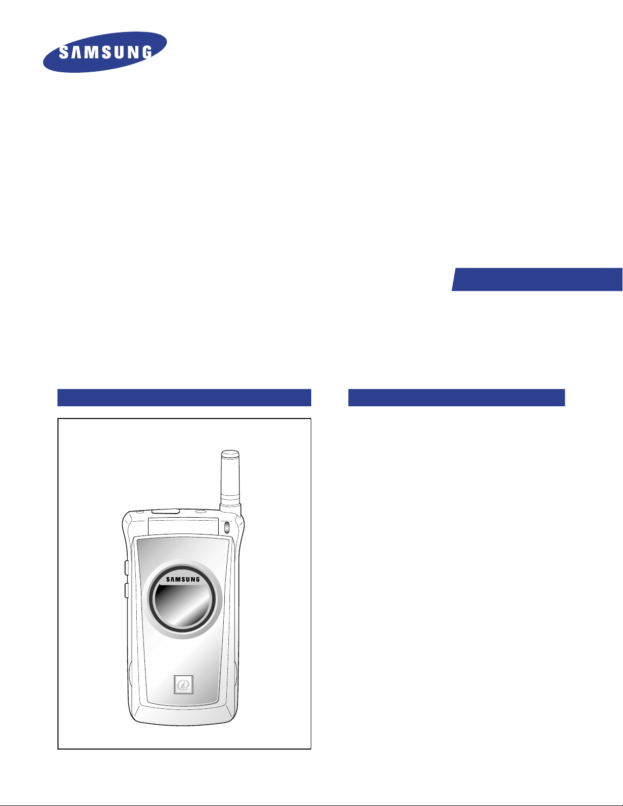
Samsung SCH-A302 Service Manual
SERVICE
Cellular Phone
SCH-A302
Manual
Cellular Phone CONTENTS
1. Specification
2. Trouble Shooting
3. Tune-up Procedure &
Test Procedure list
4. Frequency Synthesizer Circuit &
Spurious Radiation
Suppression Circuit
5. NAM Programming
6. Electrical Parts List
7. Exploded Views & Parts List
8. Block Diagram
9. PCB Diagrams
10. Circuit Description &
Circuit Diagrams

©Samsung Electronics Co.,Ltd. December. 2001
Pinted in Korea.
Code No.: GH68-02488A
BASIC.
ELECTRONICS

1. SCH-A302 Specification (REF TIA/EIA/IS-137-A-1)
1. GENERAL
SAMSUNG Proprietary-Contents may change without notice
1-1
ITEM CDMA
TX Freq. Range 824 ~ 849 MHz
RX Freq. Range 869 ~ 894 MHz
Channel Bandwidth 1.23 MHz
Channel Spacing 30 kHz
Number of Channels 20 FA
Duplex Separation 45 MHz
In/Output Impedance 50 Ω
TX Intermediate Freq. 130.38 MHz
RX Intermediate Freq. 85.38 MHz
TX Local Freq. 1st(F
TX + 130.38 MHz)
2nd(260.76 MHz)
RX Local Freq. 1st(F
TX + 210.38 MHz)
2nd(170.76 MHz)
TCXO freq. 19.68 MHz
Freq. Stability (FRX - 45 MHz) ± 350 Hz
Operating Temperature -30 °C ~ +60 °C
Supply Voltage + 3.8 V
SMALL : 81 x 42 x 21 mm 84 g
Size and Weight MIDDLE : 81 x 42 x 22 mm 87 g
LARGE : 81 x 42 x 25 mm 98 g

SAMSUNG Proprietary-Contents may change without notice
1-2
SCH-A302 Specification
2. 800 MHz CDMA
2-1. GENERAL
TX Freq. Range 824 ~ 849 MHz
RX Freq. Range 869 ~ 894 MHz
Channel Bandwidth 1.23 MHz
Channel Spacing 30 kHz
Number of Channels 20 FA
Duplex Separation 45 MHz
In/Output Impedance 50 Ω
TX Intermediate Frequency 130.38 MHz
RX Intermediate Frequency 85.38 MHz
TX Local Frequency 1st (F
TX + 130.38 MHz)
2nd (260.76 MHz)
RX Local Frequency 1st (F
RX + 85.38 MHz)
2nd (170.76 MHz)
TCXO Frequency 19.68 MHz
Freq. Stability (FRX - 45 MHz) ± 150 Hz
Operating Temperature -30 °C ~ +60 °C
Supply Voltage + 3.8 V
2-2. TRANSMITTER
Waveform Quality 0.944 or more
Open Loop Power Control
-25 dBm -57.5 dBm ~ -38.5 dBm
-65 dBm -17.5 dBm ~ +1.5 dBm
-104 dBm +18.0 dBm ~ +30.0 dBm
Minimum TX Power Control Below -50 dBm
Closed Loop TX Power Control Range ± 24 dB
Maximum RF Output Power 200 mW (+24.5 dBm)
Occupied Band Width 1.32 MHz
Conducted Spurious Emission @900 kHz -42 dBc / 30 kHz
@1.25 MHz -54 dBc / 30 kHz

SAMSUNG Proprietary-Contents may change without notice
1-3
SCH-A302 Specification
2-3. RECEIVER
Rx Sensitivity and Dynamic Range -104 dBm, FER=0.5 % or less
-25 dBm, FER=0.5 % or less
Conducted Spurious Emission
869 ~ 894 MHz < -81 dBm
824 ~ 849 MHz < -61 dBm
All other Frequencies < -47 dBm
Single Tone Desensitization
Rx Power level -101 dBm
Tone Power level -30 dBm Lower than 1 %
Tone Offset from Carrier ± 900 kHz
Intermoculation Spurious Response Attenuation
Tone 1 offset from carrier = ± 900 kHz
Tone 2 offset from carrier = ± 1,700 kHz
-Test 1, 2
Rx power = -101 dBm
Tone 1 power = -43 dBm
Tone 2 power = -43 dBm
-Test 3, 4 Lower than 1 %
Rx power = -90 dBm
Tone 1 power = -32 dBm
Tone 2 power = -32 dBm
-Test 5, 6
Rx power = -79 dBm
Tone 1 power = -21 dBm
Tone 2 power = -21 dBm
SAMSUNG Proprietary-Contents may change without notice
2-1
2. SCH-A302 Trouble Shooting
1. Logic Section
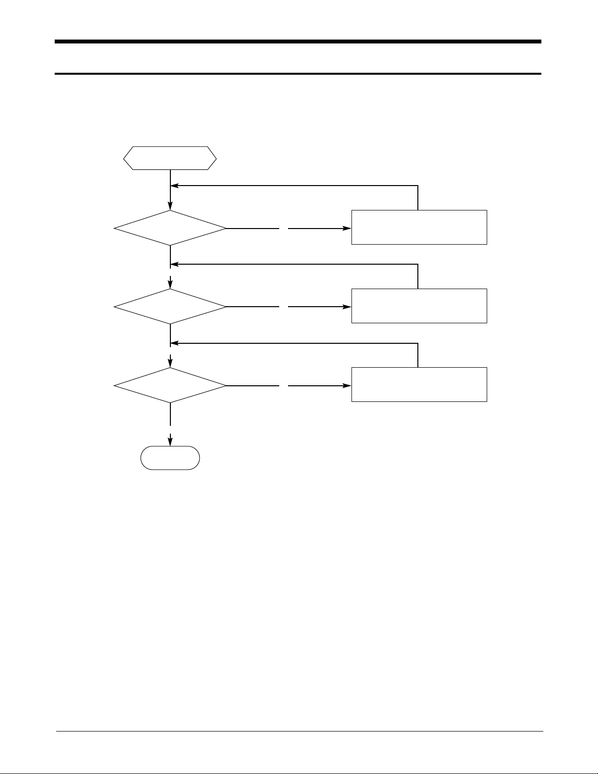
1-1. No Power
Y
U501 pin38 Input=HIGH
Check Q507, Q509 and its
neighboring circuits
N
Y
U501 pin6 & pin10
output=2.8 V?
Check U501 pin6 & pin10 and its
neighboring circuits
N
Y
U501 pin39
Input=HIGH?
Check R536 and its neighboring
circuits
N
END
Press PWR button
SAMSUNG Proprietary-Contents may change without notice
2-2
SCH-A302
Trouble Shooting
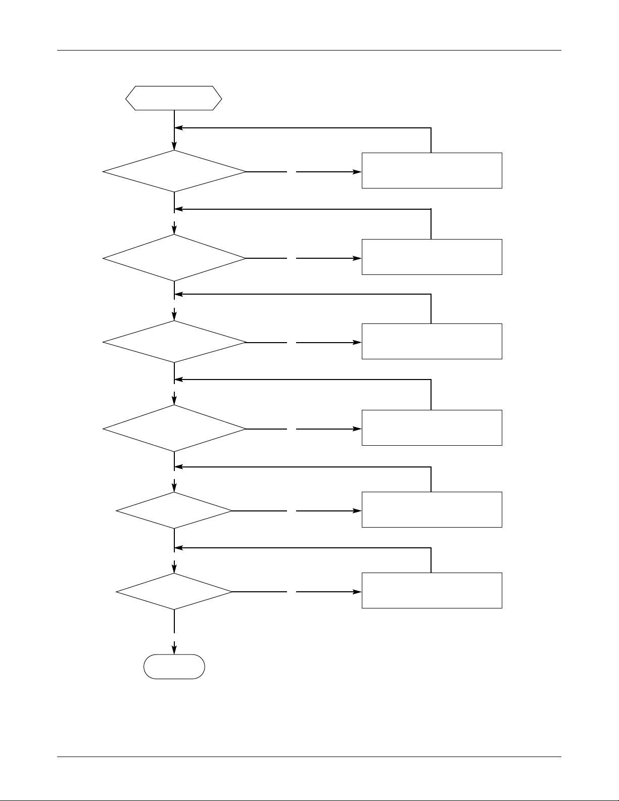
1-2. Abnormal Initial Operation
Y
TCXO CLK
applied to U609 pina17/U404
pin7?
Check VCTCXO output.
Replace if required.
N
Y
TCXO CLK
signal outputted from OSC401
pin3?
Check OSC401 and its neighboring
circuits. Replace if required.
N
Y
TCXO CL
signal outputted from OSC401
pin4?
Check OSC401 and its neighvoring
circuits. Replace if required.
N
Y
TCXO CL
signal outputted from OSC402
pin4?
Check OSC402 and its neighvoring
circuits. Replace if required.
N
Y
LED on?
Check the LED and its neighboring
circuits. Replace if required.
N
Y
Normal initial
display on LCD?
Check the LCD pins and its
neighboring circuits. Replace if
required.
N
Press PWR Key
END

SAMSUNG Proprietary-Contents may change without notice
2-3
SCH-A302
Trouble Shooting
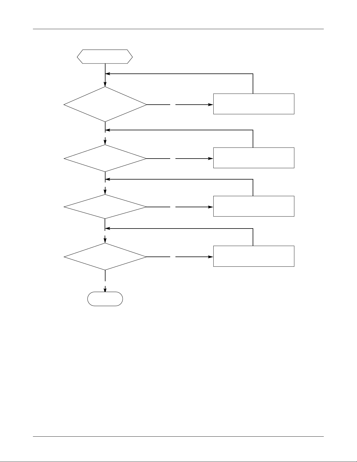
1-3. Abnormal Backlight Operation
Y
‘L’ level outputted
from U501 pin1?
Check U501 pin1 and its neighboring
circuits. Replace if required.
N
Y
‘L’ level outputted
from U501 pin2?
Check U501 pin1 and its neighboring
circuits. Replace if required.
N
Press any button on the phone
Backlight LED on
1-4. Abnormal Key Data Input
Y
Scanning signals
outputted from U609 pins C2,
A3, E4, D3, C1?
Check keypad dom switch.
Replace if required.
N
Check initial status
END
SAMSUNG Proprietary-Contents may change without notice
2-4
SCH-A302
Trouble Shooting
1-5. Abnormal Keytone
Y
CLK wavefrom outputted
from U609 pin L16 & pin M17?
Check the U609 pin and its
neighboring circuits.
Replace if required.
N
Y
CLK waveform outputted
from CON500 pin 5?
Resolder CON500 and its neighboring
circuits. Replace if required.
N
Y
Key tone waveform
applied to C561?
Check C631. Replace if required.
N
Y
Normal Keytone?
Replace the SPK assembly.
N
Abnormal Keytone
END
SAMSUNG Proprietary-Contents may change without notice
2-5
SCH-A302
Trouble Shooting
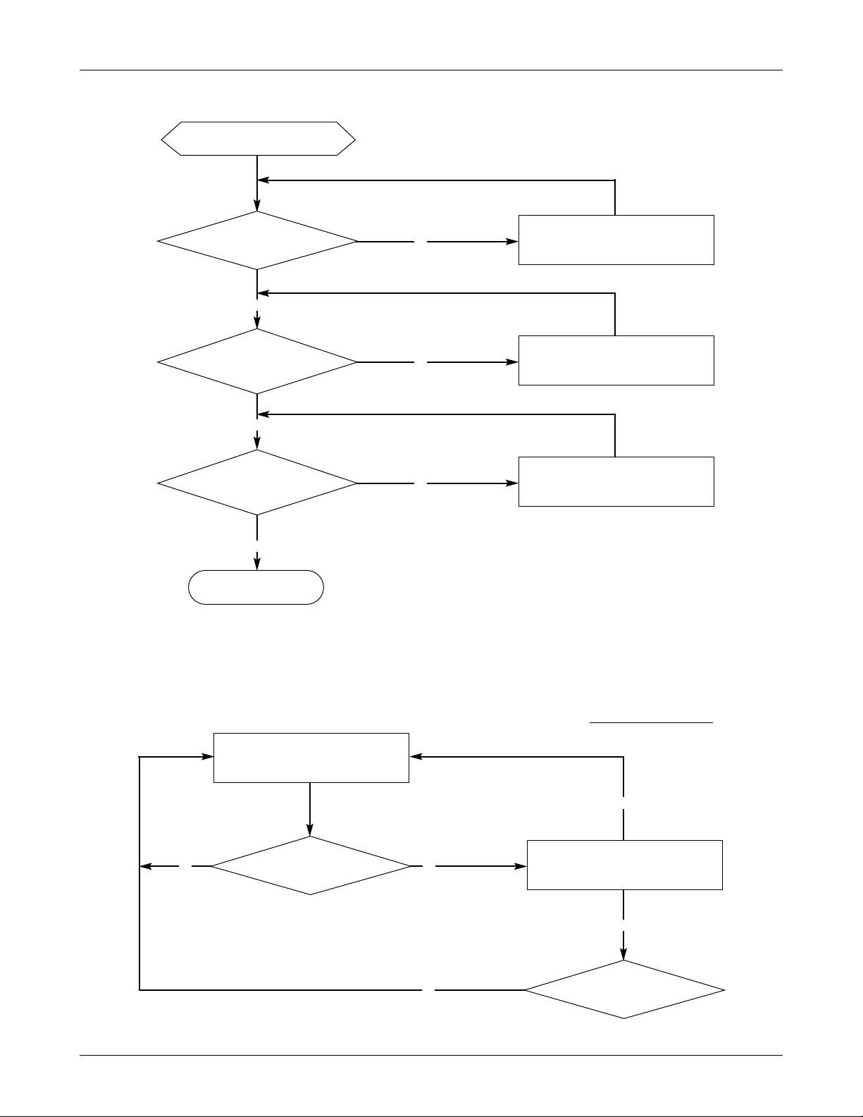
1-6. Abnormal Alert Tone
Y
CLK waveform outputted
from U609 pin C14.
Check the U609 pin and its
neighboring circuits. Replace if
required.
N
Y
CLK waveform applied to
Q511 Base?
Check R552, Q511 and its neighboring
circuits. Replace if required.
N
Y
Is the buzzer connection
correct?
Connect the buzzer correctly.
N
Abnormal Keytone
Check the buzzer and
replace if required.
2. Transmitter Section
Abormal transmitter section
Y
Turn On Max PWR
N
Check U402 local level.
Y
Check U204 TX RFT
out level OK?
N
Check U201 PWR AMP
out level OK?
N
-10~0 dBm
CDMA : 25~26 dBm
SAMSUNG Proprietary-Contents may change without notice
2-6
SCH-A302
Trouble Shooting
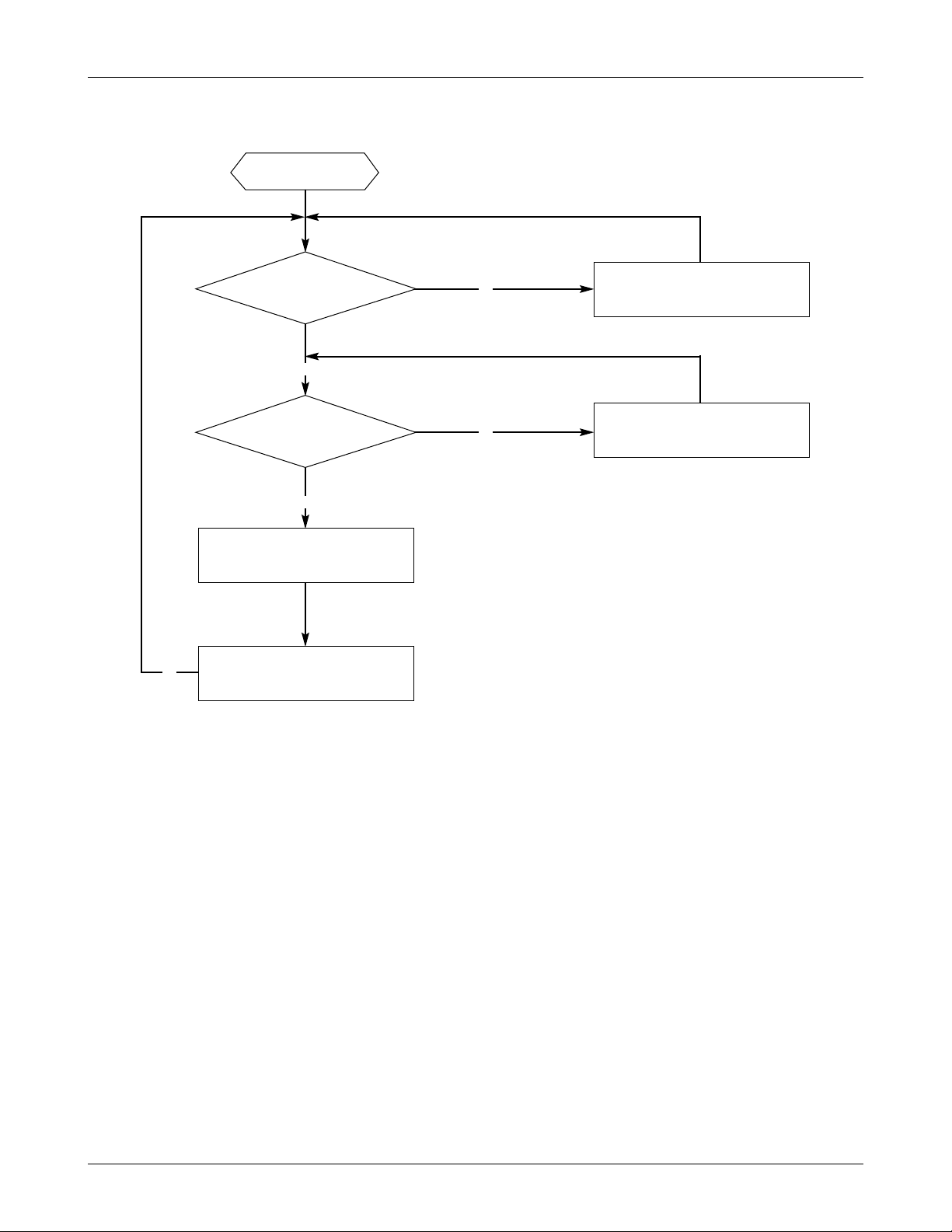
3. Receiver Section : CDMA MODE
Y
Check CDMA Rx path.
N
Y
Setup CDMA call.
OK?
Normal CDMA
SVC & ROAM OK?
Check Transmitter.
N
Start CDMA mode
Measure CDMA FER
N
Normal CDMA RF?

SAMSUNG Proprietary-Contents may change without notice
2-7
SCH-A302
Trouble Shooting
4. Repair Guide
4-1. TX Part Check Point
Using commands in test mode
-01, 09 (0363), 07, 34, 71 (380)
(1) 130.38 MHz (TX IF) output line
- RFT3100 (U204) PIN #14,#15 (about -30 dBm)
- IF TXIF problem Then Check TX 2ndLOCAL (260.76 MHz)
- TX 2ndLOCAL check - RFT 3100 PIN #19 (about 23 dBm)
(2) TXRF (824~849 MHz) out lines.
From RFT3100 (U204) pin #15 to CELLA_OUT
- F201 input and output is ok? - Pin #2 and #5 (about 16 dBm)
- PAM input is ok? U201 pin #2 (about 20 dBm)
- PAM voltage is ok? U201 pin #3 (3 V), 1,4 (3.7 V)
- PA output is ok? U201 pin #5 (about +10 dBm)
- Duplex input and out put is ok? Duplex input is same with PAM output.
Output is You can check CN302 #2 (about 10 dBm)
4-2. RX Part Check Point
(1) RX RF (869~894 MHz) Signal input lines.
- HP Equipment setting
- RF ch 363 (RX:880.89 MHz, TX:835.89 MHz)- at CALL CTRL MENU
- sctr A pwr : -25 dBm (for more easy to check use Spectrum Analyzer)
- Rf Lvl offset : -1.4 at config screen
- Spectrum Analyzer Setting
- center Freq: 880.89 MHz (when check RXRF in 363 Ch)
- span : 5 MHz
- RF input line from Duplex to Mixer check point
- CN302 input and Duplex out (You can check Duplex out at C652) is ok?
- LNA (U360)input ,output and operating voltage is ok?
:Operating voltage-pin#1 (2.5 v) in & out (#3 66 dBm,#4 49 dBm)
- F303 input and output is ok? #2,#5 (about 50 dBm)
- RX Mixer (U361) input is ok? #1 (about 49 dBm)
(2) RF IF circuit (Received RXRF Signal + 1stlocal = RX IF (85.38 MHz fixed)
- 1stlocal is ok? U361 #4,#5 (about 13 dBm)
- Voltage is ok? U361 pin #3 3.0v
- Mixer output is ok? U361 pin #6 RXIF (85.38 Mhz-fixed) (about 50 dBm)
- F301 input and output is ok?
(3) IFR (U302) neighbor circuit
- IF input is ok? U300 pin #11,12 (about 75 dBm)
- RX 2ndlocal is ok? U300 pin #21,22 (about 25 dBm)
- 3.0 V IF (3.0IF) lines are ok? IFR operating voltage

SAMSUNG Proprietary-Contents may change without notice
2-8
SCH-A302
Trouble Shooting
4-3. PLL Part Check Point
(1) VCO (Voltage Controlled Oscillator)
- Operating voltage is ok? OSC402 pin #7
- VT voltage is ok? OSC402 pin #5 (VT voltage was changed according to CH)
- Out is ok? OSC402 pin#1 output 1stlocal frequency each CH
(2) PLL(Phase Looped Lock)
- Operating voltages are ok? It use + 3.0 VR lines voltages
- TCXO_IN input is ok? U402 pin#8 It use TCXO Freq (19.68 MHz) for Reference.
4-4. Power Line Check Point
(1) U501 VBATT - #4 check
Reset - #B7 check
(2) X501 (Sleep X-tal) 32.768 MHz (pk-pk 2.7 v)
(3) TCXO(OSC401) 19.68 MHz
(4) IFR3000(U302) - #37 check TCXO-N (4.96 MHz) TCXO/N
#38 check CHIP X8-(9.84 MHz)
4-5. Reference Regulators
PM1000 U501
RESET : B7 RESET SIGNAL OUT
3.0_RX : H5 - RX CIRCUIT OPERATING VOLTAGE
3.0_TX : G5 TX CIRCUIT OPERATING VOLTAGE. (Controlled By Idle Signal)
3.0_IF : H7 RFT3100,IFR3000 AND Etc.
4-6. SAMPLING REPAIR RESULT (SCH-A302)
(1) No.1 : 24108148669 Tx Power Problem
- TX IF does not out from RFT3100 (U204) pin#1,2.
- 2ndlocal and operating voltages (3.0 IF,3.0 VR,VDC) are ok.
- Estimated factor: IFT After replace IFT It working ok.
(2) No.2 : 24108205255 - Tx Power Problem
- TX IF does not out from RFT3100 (U402)pin#6,7.
- 2
nd
local and operating voltages (3.0_MP, 3.0_TX, 3.0_TX_IF, 3.0_TXRF, 3.0_TX_LO) are ok.
- PA ON signal does not out from MSM.
- MSM also failed to J-TAG Tester.
- Estimated factor: MSM defect

SAMSUNG Proprietary-Contents may change without notice
2-9
SCH-A302
Trouble Shooting
(3) No.3 : 24108167813 - Tx Power Problem
- All TX path is good from RFT 3100 to Mixer input port.
- Mixer output is lower than normal status.
- 1
st
local and operating voltages are ok.
- TX AGC ADJ voltage is too low.
- Estimated factor: Chip capacitor (C203) which connect to TX AGC ADJ
voltage line C203 Replace ok.
(4) No.4 : Tx Power Problem
- All TX path and voltages are ok from Duplex input to RFT3100 input
- CELLA_OUT (-pin#17) is ok, But U201 RF_IN (-pin#2)is not good.
- Estimated factor : F201 Replace ok.
(5) No.5 : 24108146584 When touch MSM, RX RSSI value has lost.
- All RX path is good from Duplex to Mixer input port .
- 1
st
local & TCXO did not oscillate.
- TCXO upper case pushed then case and inside components were short when B'D is twisted.
Estimated factor : TCXO After replace TCXO It working ok.
(6) No.6 : 24108221088 - Problem with display (When power on, display was abnormal working)
- LCD and neighbor patterns are ok.
- Estimated Factor: Broken data which is in E2PROM. Data Rebuilding OK
(7) No.7 : 24108134768 - RX problem (No SVC)
- Handset doe not acquire SVC then searching CH repeat very quickly.
- All RX value is good at Rx Part Check Point.
- Ec/Io value (in debug screen) is bad.
- Estimated factor : MSM does not decode receiving signal.
(8) No.8 : No Power on (Can't not power on)
- X501 Sleep X-tal (32.768 MHz) is O.K
- V_DC 3.0V is O.K
- CHIP X8 No output IFR #38
- TCXO_N No output IFR #37
- TCXO Not oscillator Pin # 3
- TCXO crack : TCXO replace O.K
(9) No.9 : 24108233382 - ESN INVALID
- ESN No was broken : 0000000
- ESN data at E2PROM was broken caused ESD or Electric shock.
- E2PROM replace and rewriting ESN number.

3. S CH-A302 Tune-up Rrocedure & Test Procedure list
1. List of Equipment
•
DC Power Supply
• Test Jig : HHP I/F TESTJIG GH80-10502C
• Test Cable : GH3900052A
• RF Cable : GH3900075A
• CDMA Mobile Station Test Set HP8924C, HP83236A, CMD-80, etc
•
Spectrum Analyzer(include CDMATest Mode) HP8596E
2. Configuration of Test
SAMSUNG Proprietary-Contents may change without notice
3-1
RF cable
DUT
Data cable
Test Jig
T o A-Out
T o A-In
Directional
Coupler
DC Power Supply
(+3.93 V)
RF
IN/OUT
Audio
OUT
Audio
IN
HP8924C
RF IN
Spectrum Analyzer
• CAUTION : The test jig and data cable has a voltage drop of 0.15 V at FM Max power output,
you’d better set the DC power supply is 3.8 V for normal test condition.
(Nominal voltage of battery is 3.8 V at cellular phone)
SAMSUNG Proprietary-Contents may change without notice
3-2
SCH-A302 Tune-up Rrocedure & Test Procedure list
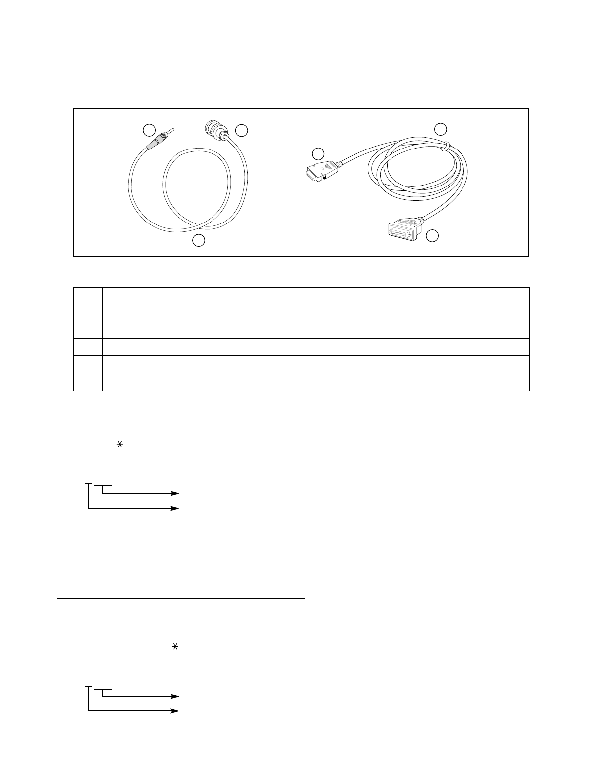
3-2. Test Cable Connections
1 MHC 172
2 RF CABLE (1.4 dB Loss for CDMA800 and AMPS, 2.1 dB Loss for PCS)
3 BNC CONECTOR (RF)
4 PLUG CONNECT TO SCH-A302
5 DATA CABLE
6 Dsub 25PIN CONNECTOR (DATA)
3. Test Cable Description for SCH-A302
3-1. Test Cable
1
2
3
4
5
6
Change to T
est Mode
A. To Change the phone’s state from Normal Mode to Test Mode, You should enter the following keys.
: Press [ 7 5 9 # 8 1 3 5 8 0 "(A+Y)"]
B. The Command “2 1” is mode and channel change.
“20363”
Channel number
Mode : CDMA
and Push the [OK] Key to save.
C. The command “0 1” is Suspend.
D. To finish the Test Mode, You should enter the command “0 2”.
Channel Selection and Tx Power Output Level Control
1. CDMA
A. Enter to Test Mode [ 7 5 9 # 8 1 3 5 8 0 "(A+Y)"]
B. The command “2 1” is mode and channel change.
“20363”
Channel number
Mode : CDMA
Push the [OK] Key to save.
 Loading...