

Samsung SCH-2000 Service Manual
C D M A P O R TA B L E
Manual
PCS T E L E P H O N E
SCH-2000
S E RVICE
CDMA PORTABLE PCS TELEPHONE
CONTENTS
1. Specification
2. Installation
3. NAM Programming
4. Circuit Description
5. Test Procedure
6. Troubleshooting
7. Exploded Views and Parts List
8. PCB Diagrams
9. Electrical Parts List
10. Block & Circuit Diagrams
Samsung Electronics Co.,Ltd.
GH68-60692A
Printed in Korea.

1. Specification
1-1 General
Frequency Range
Transmitter : 1850 ° ≠1910 MHz
Receiver : 1930 ° ≠1990 MHz
Channel Bandwidth : 1.23 MHz
Channel Spacing : 50 KHz
Number of Channels : 1200
Duplex Separation : 80 MHz
Type of Emission : G7 W
Input/Output Impedance : 50 ohms
Intermediate Frequency
Transmitter : 130.38 MHz
Receiver : 210.38 MHz
Local Frequency
Transmitter : 1st (FTX-130.38), 2nd (260.76 MHz)
Receiver : 1st (FRX-210.38), 2nd (420.76 MHz)
TCXO Frequency : 19.68 MHz
Frequency Stability : (FRX - 80 MHz) °æ 150 Hz
Operating Temperature : -30 °… ° ≠+60 °…
Supply Voltage : +3.6 V
Current Consumption (Average)
Standby : 180 mA (Non-slot mode)
Talk : 480 mA (at +10 dBm)
Size and Weight
Including Standard Battery : 121.9(H)°ø50.8(W)°ø20.3(D), 138.9 g
Including Extended Battery : 121.9(H)°ø50.8(W)°ø25.4(D), 158.7 g
Samsung Electronics 1-1

Specification
1-2 Transmitter
Waveform Quality : 0.944 or more
Open Loop Power Control Range
-25 dBm : -60.5 dBm ° ≠-41.5 dBm
-65 dBm : -20.5 dBm ° ≠-1.5 dBm
-104dBm : +15.0 dBm ° ≠+30.0 dBm
Minimum Tx Power Control : -50 dBm below
Closed Loop Power Control Range : °æ24 dB
Maximum RF Output Power : 200 mW (+23 dBm)
Occupied Bandwidth : 1.23 MHz
Conducted Spurious Emissions @1.25MHz : -42 dBc/30KHz
1-3 Receiver
Rx Sensitivity and Dynamic Range : -104 dBm, FER=0.5% or less
(Rate Set 1) : -25 dBm, FER=0.5% or less
Conducted Spurious Emission
1930 ° ≠1990 MHz : <-81 dBm
1850 ° ≠1910 MHz : <-61 dBm
All Other Frequencies : <-47 dBm
Single Tone Desensitization : lower than 1%
Rx power=-101 dBm
Tone power=-30 dBm
Tone offset from carrier=°æ1.25 MHz
Intermodulation Spurious Response Attenuation : lower than 1%
Rx power=-101 dBm
Tone power 1=-43 dBm
Tone power 2=-43 dBm
Tone 1 offset from carrier=°æ1.25 MHz
Tone 2 offset from carrier=°æ2.05 MHz
1-2 Samsung Electronics
2. Installation
2-1 Installing a Battery Pack
1. To attach the battery pack after charging, align
it with the phone about 1cm (1/2") away from
its place so that the two arrows on the phone
are seen, the battery charge contacts pointing
downwards.
2. Slide the battery pack upwards until it clicks
firmly into position. The phone is now ready
to be turned on.
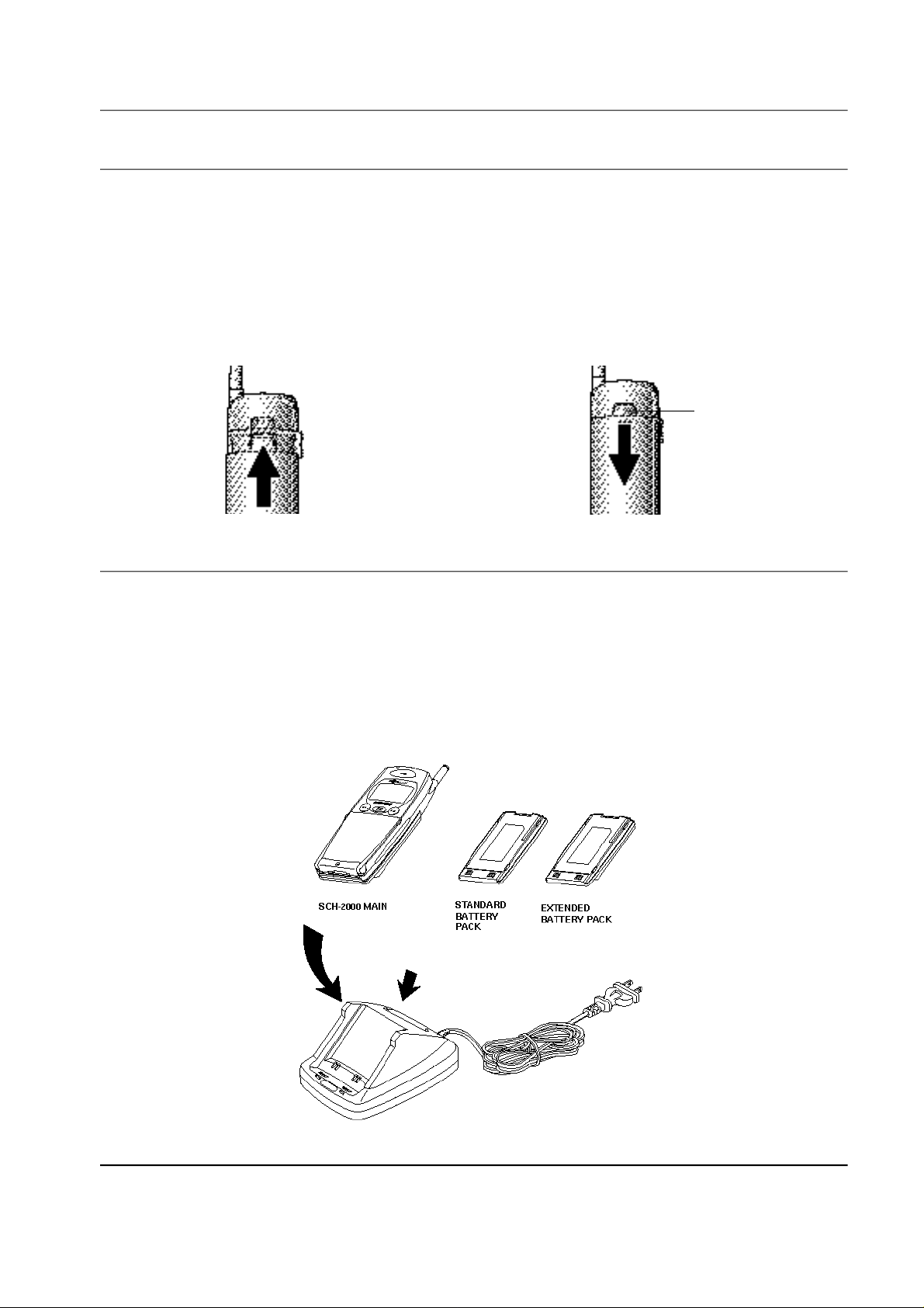
2-2 For Desk Top Use
1. Choose a proper location to install the charger
for desk top use.
2. Plug the power cord of the charger into an
appropriate wall socket. When the power cord
is connected correctly, the lamps turn on
briefly.
3. To remove the battery pack, release it by
pressing the button on the rear of the phone.
4. Slide the battery pack downwards about 1cm
(1/2") and lift it away from the phone.
Press this button to release
the battery pack
3. To charge the battery pack, insert the battery
pack into the rear slot of the charger. The lamp
marked BAT on the front panel of the charger
lights up red.
4. If you do not wish to use the phone while
charging the battery, insert the phone with the
battery pack attached into the front slot of the
charger. The lamp marked PHONE on the
front panel of the charger lights up red.
Figure 2-1 Charging The Phone and Battery
Samsung Electronics 2-1
Installation
2-3 For Mobile Mount
2-3-1 Antenna
1. Choose a proper location to install the
antenna.
¶UThe center of the roof top provides the best
performance.
¶UThe edge of the rear trunk also provides a
good performance. However, the antenna
should be higher than the roof of the car.
¶UIn case of on-glass antenna, you should
align the antenna base with the round plate
to connect the cables correctly.
2. Mount the antenna vertically, connect the
antenna cable.
3. Tighten the antenna nut fully.
2-3-2 Cradle
1. Choose a location where it is easy to reach and
does not interfere with the driver's safe
operation of the car.
2. Separate the two halves of the clamshell by
removing the two large slotted screws. See the
figure 2-2.
3. Drill holes and mount the lower half of the
clamshell by using the screws.
4. Place the cradle onto the remaining half of the
clamshell and assemble them by using the
screws.
5. Reassemble the two halves of the clamshell
together. Adjust the mounting angle and
tighten the two slotted screws.
Figure 2-2 Cradle Installation
2-2 Samsung Electronics
Installation
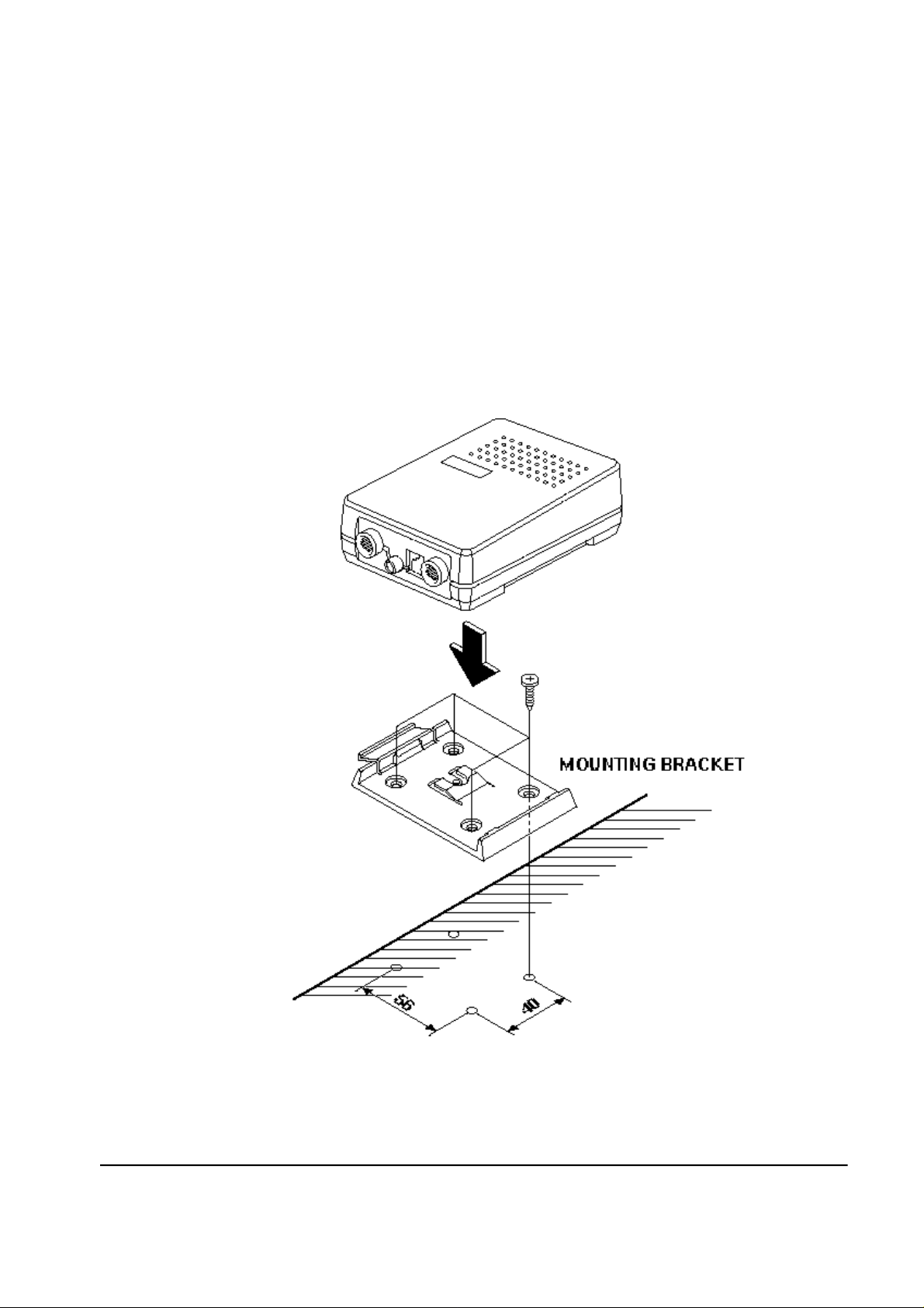
2-3-3 Hands-Free Box
1. Drill holes in a proper location for the handsfree box, attach the mounting bracket by using
the screws. See the figure 2-3.
2. Install the hands-free box into the bracket.
2-3-4 Hands-Free Microphone
1. It is recommended to install the microphone
where it is 30-45 cm (12-18") away from the
driver. Choose the location where is least
susceptible to interference caused by external
noise sources, ie, adjacent windows, radio
speakers, etc. Normal place is the sun visor.
2. Once the microphone has been correctly
positioned, connect the microphone wire to
the MIC jack on the hands-free box.
Figure 2-3 Hands-Free Box Installation
Samsung Electronics 2-3
Installation
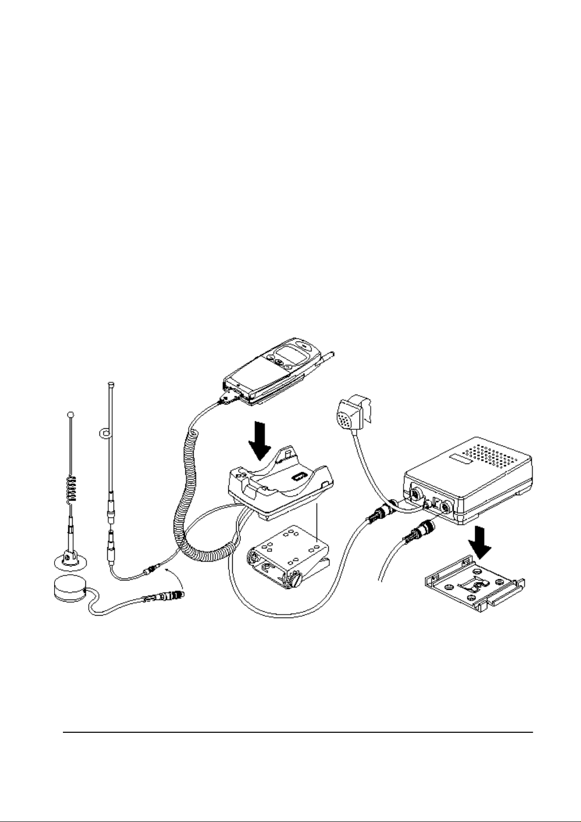
2-3-5 Cables
1. Connect the cradle and the hands-free box
with the data cable. See the figure 2-4.
2. Connect the antenna cable to the RF jack of the
cradle.
3. Connect one end of the power cable to the
battery or ignition terminal. Connect the red
wire to the battery (+) terminal, black wire to
the vehicle chassis. Then connect the battery (-)
terminal to the vehicle chassis.
4. Connect the other end of the power cable to
the PWR jack of the hands-free box.
Notes:
¶UIt is recommended to connect the power cable
directly to the battery to avoid power noise.
¶UMake sure the connection between the battery -
terminal and the vehicle chassis is made
correctly.
¶UMake sure the fuse having a proper capacity is
used on the power cable.
¶UMake sure the cables do not pass over any sharp
metal edge that may damage it.
Figure 2-4 Cable Connections
2-4 Samsung Electronics

3. NAM Programming
NAM features can be programmed as follows:
Notes:
-If you enter the NAM program mode, each item shows the currently stored data. Go to the next item by
pressing OK.
-You can modify the data by entering a new data.
-If you enter a wrong digit, press CLR to delete the last digit. Press and hold CLR to delete all digits.
-To scroll items backwards or forwards, press the VOLUME button on the left side of the phone.
3-1 General Setup
LCD Display Key in Function
MENU, 5, 0 -selects NAM programming
Enter Lock
??????
SVC Menu°Ë°È
1:PCS Phone#
2:General
ESN
B0000000
CAI version
VOC13K/8K
SO_VOICE_13K
SCM
00001010
Lock Code
0000
Slot Mode
No
6-digit code -Enter random 6-digit code (MSL)
2 -choose 'GENERAL.'
Volume °„ -Electronic Serial Number of the phone is displayed
Volume °„ -Common Air Interface version is displayed
1
°Ëor°È -Select vocoder service option
OK -stores it
Volume °„ -Station Class Mark displays the power class,
transmission, slotted class, dual mode.
Lock code, current status is displayed
4-digit code -to change, enter new code.
OK -stores it.
Slot mode. 'Yes' indicates the slot mode.
°Ëor°È -changes the status.
OK -stores it.
Slot Index
2
Samsung Electronics 3-1
0 - 7 -to change, enter new one.
OK -stores it.
Slot mode index. The higher, the longer sleeping time.

NAM Programming
3-2 Setting Up NAM
LCD Display Key in Function
SVC Menu°Ë°È
1:PCS Phone #
2:General
Volume °„ -NAM Programming Menu is displayed
SVC Menu°Ë°È
3:NAM
IMSI_MCC
310
IMSI_MNC
00
CDMA ACCOLC
CDMA HomeSID
Yes
CDMA fSID
Yes
CDMA fNID
Yes
3 -choose 'Setup NAM'
number IMSI Mobile Country Code, current code is displayed.
OK -to change, enter new one.
-stores it.
number IMSI Mobile Network Code, current code is displayed.
OK -to change, enter new one.
-stores it.
CDMA Access Over load Class, current status is displayed.
0
class number -to change, enter new one.
OK -stores it.
CDMA Home system ID, current status is displayed.
°Ëor°È -changes the status.
OK -stores it.
CDMA foreign SID, current status is displayed.
°Ëor°È -changes the status.
OK -stores it.
CDMA foreign NID, current status is displayed.
°Ëor°È -changes the system.
OK -stores it.
SID
4120
NID
65535
3-2 Samsung Electronics
number -to change, enter new one.
OK -stores it.
number -to change, enter new one.
OK -stores it.
first SID written in the list, current status is displayed.
first NID written in the list, current status is displayed.

4. Circuit Description
4-1 Logic Section
4-1-1 Power Supply
With the battery installed on the phone and by
pressing the PWR key, the VBATT and ON_SW
signals will be connected. This will turn on
Q109(2SC4081) and make gate port Low. VBAT
will be supplied to input if DC/DC converter,
controlled by Q115, makes 3.6V for Idle and Talk
Mode, and 3.4V for Sleep Mode.
The VBAT applied to ON_SW turns on
Q110(DTC144) and will result in the signal
ON_SW_SENSE to change state from HIGH to
LOW. The MSM recognizes this signal and sends
out PS_HOLD(logical HIGH) to turn on Q109 even
after the PWR key is released.
The power from U108 is used in the digital part of
MSM and BBA. The power from U111 is used in
the analog part of BBA.
4-1-2 Logic Part
The Logic part consists of internal CPU of MSM,
RAM, ROM and EEPROM. The MSM receives
TCXO/4 and CHIPX8 clock signals from the BBA
and controls the phone. The major components are
as follows:
¶UCPU : INTEL 80186 core
¶UFROM : U111,U114 (MBM29LV800T)-8MBIT
FLASH ROM
¶USRAM : U112(KM68FS2000I)-2MBIT STATIC
RAM
¶UEEPROM : U107(24LC128I)-128KBIT SERIAL
EEPROM
FLASH ROM (U111, U114)
One 8MBIT FROM(U111) is used to store the
terminal's program. Using the down-loading
program, the program can be changes even after
the terminal is fully assembled. The other is used
to store program for Voice memo, Voice dialing
and so on.
SRAM (U112)
One 2MBIT is used to store the internal flag
information, call processing data, and time data.
EEPROM (U107)
One 128KBIT is used to store ESN, NAM, power
level, volume level, and telephone number.
KEY-PAD
For key recognition, key matrix is setup using
SCAN0-6 of STROBE signals and KEY0-2 of input
ports of MSM. Six LEDs and backlight circuitry are
included in the keypad for easy operation in the
dark and it senses the six LEDs and backlight flip
ON/OFF through reed switch.
EARPIECE
This is a phone that can make a call and receive a
call by earpiece.
LCD MODULE
CPU
LCD module contains a controller which will
INTEL 80186 CMOS type 16-bit microprocessor is
used and CPU controls all the circuitry. For the
CPU clock, 27MHz is used.
Samsung Electronics 4-1
display the information onto the LCD by 8-bit data
from the MSM. It also consists a DC-DC converter
to supply negative voltage for fine view angle and
LCD reflector to improve the display efficiency.

Circuit Description
4-1-3 Base Band
MOBILE SYSTEM MODEM (MSM)
The MSM equipped with the INTEL 80186 CPU
core is an important component of the CDMA
cellular phone. The MSM comes in a 176 pins
TQFP package. The interface block diagram is
shown on Figure 4-1.
MICROPROCESSOR INTERFACE
The interface circuitry consists of reset address bus
(A0-A19), data bus (AD0-AD15), and memory
controls (DT-R,HWR/,LWR/,RAM_CS/,
ROM_CS).
INPUT CLOCK
°§CPU clock : 27 MHz
°§TXCO/4 (pin34) : 4.92 MHz. This clock signal
from the BBA is the reference clock for the MSM
except in CDMA mode.
°§CHIPX8 : 9.8304 MHz. The reference clock used
during the CDMA mode.
ADC Interface
ADC_CLK (pin3), ADC_ENABLE (pin1) and
ADC_DATA (pin2) are required to control the
internal ADC in the BBA.
Data Port Interface
Includes the UART. Also, supports Diagnostic
Monitor (DM) and HP equipment Interface.
CODEC Interface
The MSM outputs 2.048MHz PCM_CLK (pin19)
and 8KHz CODEC_SYNC (pin16,20) to the
CODEC (U102). The voice PCM data from the
MSM (U101)PCM_DIN (pin135) is compressed
into 8KHz by QCELP algorithm in the CDMA
mode.
RF Interface
BBA INTERFACE
CDMA,Data Interface
°§TX_IQDATA0~7 (pin24-32) : TX data bus used
during both CDMA.
°§C_RX_IDATA0-3 (pins16-20) and
C_RX_QDATA0-3(pins 12-15) : RX data bus
used during CDMA mode.
Clock
°§TX_CLK(pin 22), TX_CLK/(pin23) : Analog to
Digital Converter(ADC) reference clock used in
TX mode.
°§CHIPX8 : ADC reference clock used in CDMA
RX mode.
TX : TX_AGC_ADJ (pin35) port is used to control
the TX power level and PA_ON (pin44) signal is
used to control the power amplifier.
RX : AGC_REF (pin36) port is used to control the
RX gain and TRK_LO_ADJ (pin45) is used to
compensate the TCXO clock.
General Purpose I/O Register Pins
Input/output ports to control external devices.
Power Down Control
When the IDLE/signal turns LOW, only the TX
sections will be disabled. If both the IDLE/ and
SLEEP/ changed to LOW, all the pins except for
the TXCO are disabled.
4-2 Samsung Electronics

Circuit Description
Figure 4-1 Baseband Block Diagram
4-1-4 Audio Section
TX AUDIO PATH
The voice signal output from microphone is
filtered and amplified by the internal OP-AMP
and is converted to PCM data by the
CODEC(U102). This signal is then applied to the
MSM(U101)'s internal vocoder.
RX AUDIO PATH
The PCM data out from the MSM is converted to
audio signal by ADC of CODEC(U102),is then
amplified by the speaker amplifier(U105) to be
sent to the speaker unit.
VOLUME ADJUST
Volume can be adjusted up to 8 steps for the user
to obtain a proper loudness of received signal.
4-1-5 Buzzer Driving Circuitry
Buzzer generates alert tone. When the buzzer
receives the timer signal from the MSM, it
generates alert tone. The buzzer level is adjusted
by the alert signal's period generated from the
MSM timer.
4-1-6 Key Tone Generator
Ring signal (pin49) from MSM(U101) is passed
through LPF consisting of R220, C222, R219, and
C221, amplified at the speaker amp(U105) and
come out to speaker.
Samsung Electronics 4-3

Circuit Description
4-2 Receiver Section
LOW NOISE AMPLIFIER (LNA)
The low noise amplifier featuring 1.6dB Noise
Figure and 19dB gain amplifies a weak signal
received from the base station to obtain the
optimum signal level.
DOWN CONVERTER (MIXER)
First local signal is applied to this down converter.
The down converter transfers the signal amplified
at the LNA into 210.38 MHz IF signal. 210.38MHz
IF signal is made by subtracting 1960°æ30MHz RF
signal from 1750°æ30MHz first local signal. The
LNA is Q303 and down converter is U302.
RF IF AUTOMATIC GAIN CONTROLLER
(AGC) AMP
210.38 MHz IF signal is applied to IF AGC
amp,the AGC output level is applied to BBA (Base
Band Asic). The AGC amp (U303) keeps the signal
at a constant level by controlling the gain.
Dynamic range is 90dB, up gain +45dB, and down
gain -45dB.
RF BAND PASS FILTER (BPF)
BUFFER
Buffer (Q311) amplifies signal to be applied to the
local input of the down converter (U302) when a
phase is locked between U304 and U305.
VOLTAGE CONTROLLED OSCILLATOR
The VCO (U305) generates the signal having
1750MHz center frequency and °æ30MHz
deviation with the voltage control. PLL IC(U304)
controls this signal.
PHASE LOCKED LOOP (PLL)
Input reference frequency is generated at
VCTCXO (U306) and the signal is generated at
VCO. PLL compares the two signals and generate
the desired signal with a pre-programmed counter
which controls voltage.
VOLTAGE CONTROLLED TEMPERATURE
COMPENSATED CRYSTAL OSCILLATOR
It provides 19.68MHz reference frequency to PLL
(U304) and BBA (U401). A correct frequency
tuning is made by the voltage control.
The RF BPF(F302) accepts only a specific
frequency (1960°æ30MHz) from the signal
received from the mobile station. The band width
is 60MHz.
IF SAW BAND PASS FILTER FOR CDMA
IF SAW BPF (F303) is used for CDMA system
having 1.23 MHz wide band and °æ630kHz band
width. The filter also eliminates the image product
generated at the mixer.
4-4 Samsung Electronics
DUPLEXER
Duplexer (F301) controls to transmit through the
antenna only the signals within acceptable Tx
frequency range (1880°æ30MHz) and to receive
through the antenna only the signals within
acceptable Rx frequency range (1960°æ30MHz). It
also matches LNA(Q303) input in receiving part
and PA output in transmitter part with the
antenna.

4-3 Transmitter Section
Circuit Description
POWER AMP MODULE
Power Amp Module (U407) amplifies signal to be
sent out to the base station through the antenna.
DRIVER AMP
The driver amp (Q413) allows the signal input to
the Power Amp Module (U407) to be within a
specified level.
UP CONVERTER (MIXER)
The up-converter (U405) receives the first local
signal to generate 1880°æ30MHz from the signal
controlled by TX AGC amp (U404). 1880°æ30MHz
signal comes out from the mixer output by adding
130MHz IF signal to 1750°æ30MHz first local
signal. The driver amp's reference number is Q413
and up converter's reference number is U405.
POWER SUPPLY SWITCHING
Power supply switching (Q412) turns on TX
POWER when the phone is in traffic mode and
supplies power to the circuits.
ISOLATOR
Isolator (I401) is used to reduce a reflected signal
to protect the power amp MMIC from being
damaged.
POWER SUPPLY REGULATOR
The power supply regulator (U413,U414) supply a
regulated power to each part of transmitter.
U413 supplies 3.6V to Tx driver (Q413) and Power
Amp Module (U407). U414 supplies 3.3V to the
others.
IF AUTOMATIC GAIN CONTROLLER AMP
The signal out to BBA (Base Band Asic) should be
a constant level. The TX IF AGC amp (U404)
controls power to keep the signal at a constant
level. Dynamic range is 85 dB, up gain +40dB, and
down gain -45dB.
ANTENNA
ANT1 allows signals to send to receive from the
base station.
RF BAND PASS FILTER (BPF)
The RF BPF (F402) accept only a specific frequency
(1880°æ30MHz) to send it out to power amp
MMIC. The band width is 60MHz.
Samsung Electronics 4-5

Circuit Description
4-4 Hands-Free Kit
Hands-free board is largely composed of car
adapter circuit and Hands-free circuit.
4-4-1 Car Adapter Circuit
POWER SUPPLY
Input power switching circuit : This circuit (Q902,
Q903) is power switching control circuit. It supply
power for hands-free kit.
8V regulator (U806) : This circuit supplied power
for audio amplifier (+8V).
Vcc regulator (U807) : This circuit regulate Vcc
(+5V).
CHARGER CIRCUIT
This circuit charges battery pack by detecting the
temperature of battery, the slope of temperature,
the slope of the voltage of battery, charging time,
etc.
During charging time turns on red LED. Charging
is completed, turn on green LED.
Voltage detection circuit : Charging circuit is
designed to stop charging when the charging
circuit is decrease.
The voltage of battery is entered to A/D converter
located in U701 #4. (B/VTG)
Temperature detection circuit : The temperature
of battery is measured by missing NTC thermistor.
NTC thermistor has a characteristics of Log-scale.
It can obtain a linear characteristics by the parallel
connection of resistors.
4-4-2 Hands-free Circuit
POWER SUPPLY (U808)
U808 regulated -5V.
TX PATH
The audio signal from external Mic(J701) flows
into U802 #11. U802 include amplifier and Control
circuit for hands-free operating. U801A amplified
input signal. Output signal transmit to HHP.
RX PATH
Battery Type Capacity Charge Time Charge Current
S t a n d a r d 1 0 0 0 m A H about 3h °æ3 0 M OA ~ 900mA
E x t e n d e d 1 6 0 0 m A H about 5h °æ3 0 M OA ~ 900mA
4-6 Samsung Electronics
Input audio signal canceled noise by difference
amplifier (U801c). U802 process hands-free action.
The RX audio signal is input (U805). The speaker
drive amp (U804) amplify the Rx audio signal and
the output of U804 is go out of speaker.

4-5 Desk-Top Rapid Charger
Circuit Description
4-5-1 Description
This specification describes requirements of
DTC55 desktop charger. DTC55 is designed as
desk-top rapid charger for Li-ion battery for
SAMSUNG PCS Cellular phone SCH2000.
This charger include AC/DC adapter circuitry in
its own board. This characteristic offers operating
with direct indoor AC input without additional
AC/DC adapter unit.
Integrated AC/DC adapter circuitry adopts
switching mode power supply to keep lightness of
whole charger.
And it has two battery slot, the front one is
intended for cellular phone with battery and rear
one is for another battery only. Two bi-color LED
include charging status of each battery slot.
Charging current is automatically controlled by
programmed microprocessor inside of charger, to
proper to each type of battery.
4-5-2 Electrical Characteristic
AC IN PUT
¶UAC input voltage : 110/220Vac
¶UAC input voltage : 85Vac ~ 264Vac
¶UAC input frequency : 60Hz
¶UAC input ON/OFF cycle : MIN 5 sec
OUT PUT
¶UBattery Charging Method : CC-CV mode
¶UBattery Charging Current Range under CC
mode
-Front slot : 800mA °æ70mA
-Rear slot : 400mA °æ50mA
¶UBattery Charging Voltage Range under CC
mode
-Front slot voltage setting (V/F : 5.1K)
4.1 °æ0.05 VDC with 110Vac input and 180mA
load current.
- CV mode 4.05V ~ 4.15V
- Voltage range (4.05V ~ 4.15V), is to be tested
with 180mA ~ 600mA load range for Front slot.
- Rear slot voltage (V/F : 5.1K)
- CV mode 4.0V ~ 4.15V at 150mA load
¶URipple & Noise
- Ripple & Noise Lim it : 60mVp_p MAX
- Test Condition
- Front : At output contact with 20MHz
bandwidth using resistive load 650mA and
nominal input.
¶UEfficiency
- 55% MIN
- Efficiency is to be tested with 650mA and
150mA resisted load and 110Vac input.
Samsung Electronics 4-7

Circuit Description
LED INDICATION
¶UAC plug in : red and green orange at 0.5 sec
intervals
¶USlot Identification
- Front slot : LED “ PHONE”
- Rear slot : LED "BATT”
¶UCharging Status
- Constant Red : Rapid charging
- Constant Green : Rapid charging is terminated.
- Constant Orange : Under or Over Temperature
- Flashing Orange
*If charging is started with any battery of open
cell, equivalent LED should be flashing
Orange.
*If a battery of open cell is loaded on rear slot
whole front slot is charging, the other good
battery.
LED for front slot - Constant RED
LED fro rear slot - flashing Orange
*If a battery of open cell is loaded on front slot
while rear slot charging, the other good
battery.
LED for front slot - flashing Orange
LED for rear slot - constant RED
- Off : battery unloaded
BURN -IN
¶UAll power supply shall be subjected to the burn -
in process
- Temperature : 35 °∆C °æ5 °∆C
- Load condition : 600mA and 150mA
- Input Voltage : nominal 110Vac
4-5-4 Schematic Description
BATTERY RECOGNITION CIRCUIT : HIC
¶UBattery identity detection determined to voltage
through R4, R6, R11, R12.
¶UBattery internal between C/F and GND.
CURRENT DETECTION CIRCUIT : R5, R6,
R11, R12, HIC
¶UBattery charging current is changed voltage
detection.
¶UThis voltage inputted u-COM to 16 times
amplified through HIC.
4-5-3 General Characteristics
TEMPERATURE
¶UCharging Temperature Range : 0 to 45 °∆C
¶UStorage Temperature Range : -20 to 85 °∆C
SAFETY REQUIREMENTS
¶USafety Approval
- Approval No. : UL and CUL, FCC Class B
- Approval No. should be appeared in label
design.
PRIMARY - SECONDARY ISOLATION
¶UWithstanding Voltage : 3K Vdc for 1 sec
¶UCut-off Current : 10mA
VOLTAGE DETECTION CIRCUIT : HIC
u-COM A/D through HIC pin 12, 13 detected
voltage.
BATTERY TEMPERATURE DETECTION
CIRCUIT : HIC, TH1
Battery temperature detection determined
temperature by use of thermistor resistor variation
of TH1 by HIC.
CURRENT LIMIT CIRCUIT : HIC
When soft-change, current detection circuit limited
current flow to battery, reference voltage more
than detected current, detected current and HIC
internal reference voltage.
4-8 Samsung Electronics

4-6 Cigarette Lighter Adapter
4-6-1 Description
Circuit Description
This specification describes requirements of
CHG55 cigarette lighter adapter. CHG55 is
designed as an charger for Li-ion battery for
SAMSUNG PCS Phone SCH-2000.
4-6-2 Electrical Characteristic
¶UInput Voltage : 11~ 30V DC (Normal voltage :
13.7V DC)
¶UOutput Voltage : 4.1 °æ0.02V DC9 (Maximum)
¶UOutput Current :
- Output Current : 0 ~ 740 mA
- Current limited in this unit should be kept 740
°æ40mA
¶URipple Noise : 0.1 Vp_p (under 600mA load)
¶UFuse Capacity : 250V, 2A
¶UCharging time :
- Standard battery : 4 hours °æ30 minutes
- Extended battery : 5 hours °æ30 minutes
AUTO POWER ON
When a phone is connected to CLA, the power of
the phone will be on automatically.
DUAL LED
This CLA has dual LED.
Green : When battery is fully charged. (over 80%)
Red : When CLA is on charging battery.
4-6-4 Schematic Description
POWER SUPPLY
This circuit supplies HHP & battery with power
received from Cigar Lighter jack of automobile.
POWER CIRCUIT OF CHARGE FOR HHP
POWER & BATTERY
4-6-3 Function
PROTECTION CIRCUIT
Protection Circuit is the circuit against the
electrical stress which is occurred at unexpected
condition of the source power of CLA unit such as
reserve voltage or over current.
DETECTION OF MOBILE PHONE
If mobile phone is connected to CLA, the CLA
lamp is on to display whether CLA is operating or
not.
This Switching Regulator produces needed power
for charging HHP power & battery, supplied U1,
D1, D2, C1, C2, L1, R11 from Cigar Lighter jack of
automobile.
CONFIRMING CIRCUIT OF EXISTING
BATTERY OR NOT
U3A reads separated voltage between resistance
battery C/F and R20, controls no. 5 pin of U1
through reference voltage and comparator then
decides to produce Vcc or not.
CHARGE CURRENT CONTROL CIRCUIT
U2A, U4, Q1 and side circuit detects R4's flowing
current, control no. 5 pin of u1 then charge current
and charge voltage.
Samsung Electronics 4-9
Circuit Description
LED ACTIVATING CIRCUIT
LED activating circuit compares to voltage
difference between R4 source and D4 PROP,
controls Q3, Q4 through U2B comparator for Q6
and side circuit, then activates LED.
AUTO POWER ON CIRCUIT
Q7, Q8 and side circuit makes power on the circuit
allowed Vcc power to no. 9 HHP pin (power on)
by turned on Q7, following up the producing Vcc.
CONNECTION OF CLC, CURL, AND CABLE
PIN NO.(CLA)
#1 HP-PWR 9
#2 V-BAT 14/15/16
#3 V/F N.C
#4 C/F 3
#5 GND 2/4/6
DESCRIPTION
PIN NO.(PHONE)
4-10 Samsung Electronics

4-7 Travel Charger
4-7-1 Description
- This specification describes requirements of TC55
travel charger. TC55 is designed as a wall-mount
type rapid charger for Li-ion battery (1CELL) for
SAMSUNG PCS phone SCH-2000.
- This charger includes AC/DC adapter circuitry
in its own board. This characteristic offers
operating with direct indoor AC input without
additional AC/DC adapter unit. And it is
connected by DC power cord to a phone with
battery.
- Integrated AC/DC adapter circuity adopts
switching mode power supply to keep lightness
of whole charger.
- Own bi-color LED indicates charging status of
battery.
Circuit Description
SAFETY REQUIREMENTS
Primary-Secondary Isolation
- Withstanding Voltage : 3000Vac min for 1 second
- Cut-put current : 10mA
- Isolation Resistance : 8 Mohm
LED INDICATION
AC PLUG IN : yellow for 1 second
Charging status
- Red : Charging
- Green : Charging termination
- OFF : Battery unloaded
- Yellow blinking : Error mode
- Yellow : Under or over temperature
- Charge current is automatically controlled by
programmed microprocessor inside of charger.
4-7-2 Electrical Characteristic
AC INPUT
- AC input voltage : 110/220 Vac
- AC input voltage range : 85Vac ~ 264 Vac
- AC input frequency : 60Hz
- Ac input power : 10W
OUTPUT
- Battery Charging Voltage : 4.1/4.2 V
- Battery Charging Voltage Range under C-V
mode : 4.1/4.2 (-0.2/+0.1V)
- Battery Charging Current : 0 to 700 mA
- Battery Charging Current Range under C-C
mode : 700mA °æ70 mA
- Efficiency : 55% min
- Ripple & Noise : 60mVp_p max (test condition :
At output contact with 20MHz bandwidth using
resistive load 650mA)
ENVIRONMENTAL SPECIFICATION
Unit Operating Temperature Range : 1 to 45 °∆C
Storage Temperature : -20 to 85 °∆C
4-7-3 Schematic Description
MICOM CONTROLLER : U4
¶UU4 is include u-COM to controlled whole
charging system and include following internal
circuit.
- General input / output
- A/D converter
- Reset delay circuit (power on delay)
- Timer
¶UIt is carried following functions
- Battery recognition
- Charging termination condition detection
- Output short detection and output protection
- Temperature detection
Samsung Electronics 4-11

Circuit Description
BATTERY RECOGNITION CIRCUIT : U4
¶UBattery identity detection determined to voltage
detection
¶UBattery internal between ID & GND
CURRENT DETECTION CIRCUIT : R14, R15,
R16, U4
¶UBattery charging current is changed voltage
through R14, R15, R16
¶UThis voltage inputted u-COM to 16times
amplified through U4
VOLTAGE DETECTION CIRCUIT : U4
¶Uu-COM A/D through U4 pin 15 detected
voltage
BATTERY TEMPERATURE DETECTION
CIRCUIT : U4
¶UBattery temperature detection determined
temperature by use of thermistor resistor
variation of battery by U4
CURRENT LIMIT CIRCUIT : U4
¶UWhen soft-change, current detection circuit
limited current flow to battery, reference voltage
more than detected current, detected current
and U4 internal reference voltage.
4-12 Samsung Electronics
5. Test Procedure
5-1 List of Equipment
¶UDC Power Supply
¶UTest Jig
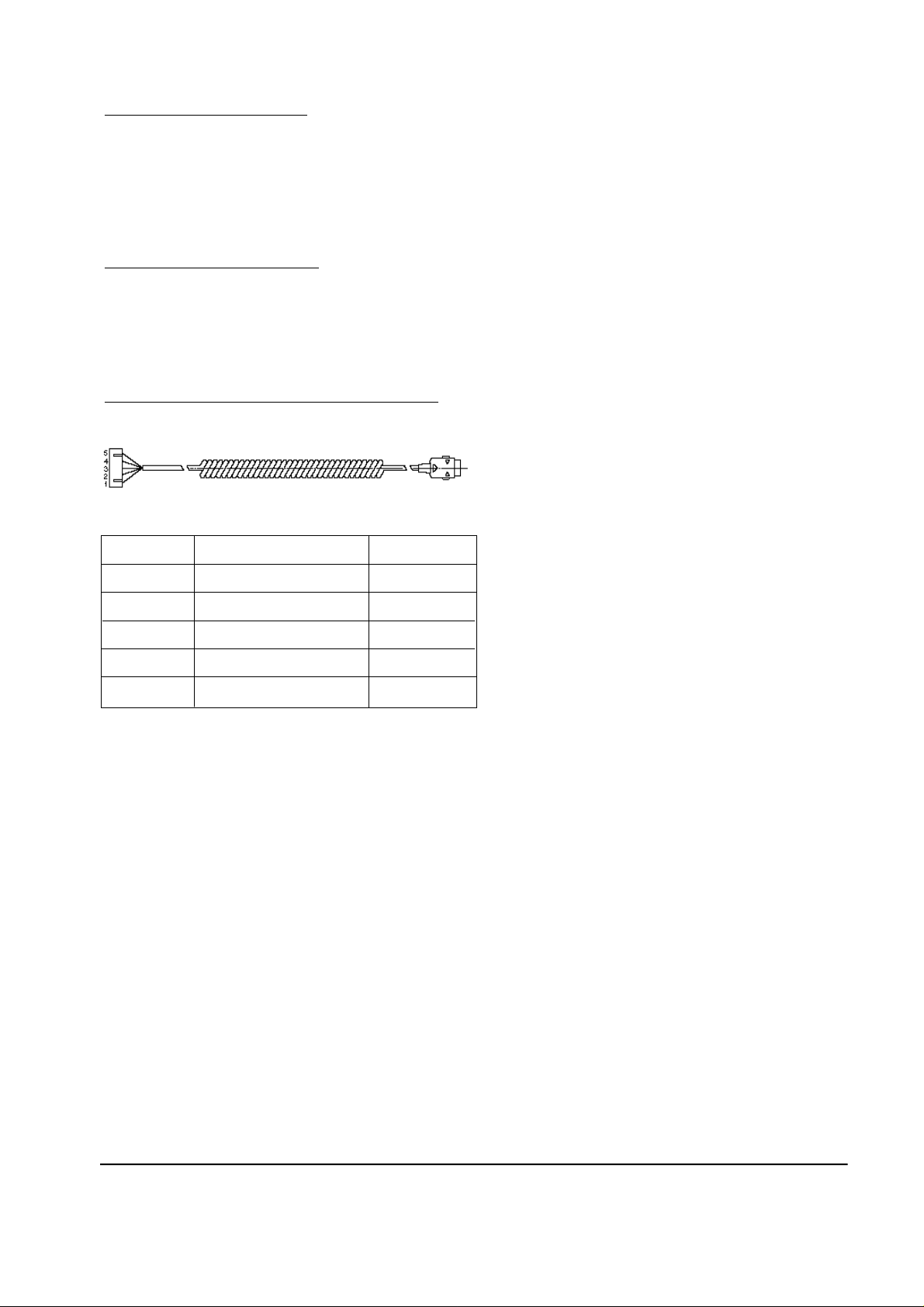
¶UTest Cable
¶UCDMA Mobile Station Test Set HP8924C, HP83236B, CMD-80, etc
¶USpectrum Analyzer (include CDMA test mode) HP8596E
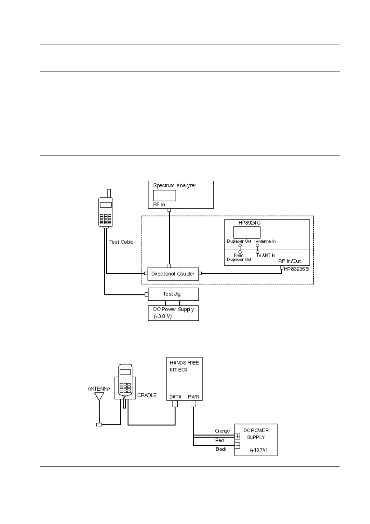
5-2 Configuration of Test
5-2-1 Hand Set
5-2-2 Hand-Free
Samsung Electronics 5-1

Test Procedure
5-3 Test Procedure
5-3-1 Change to Test Mode
1. To change the phone from Normal Mode to test
Mode, You should enter the following keys.
" 4 7 * 8 6 9 # 1 2 3 5 "
2. The command ° ∞0 1"(Suspend) is entered to start
test.
3. To finish the Test Mode, You should enter the
command "0 2".
5-3-2 Channel Selection and Tx Power
Output level Control
1. You should change the phone from Normal
Mode to Test mode
2. The command ° ∞0 1"(Suspend) is entered to start
test.
3. You should enter the following keys.
" 0 9, 0 5 2 5, #, 0 7, 3 4, 7 1, 4 7 5, #"
¶UIf you enter the command "0 9", You can select
the channel
ex) 0 9 X X X X (means channel number)
¶UThe command "0 7°±means Carrier On (Carrier
Off : ° ∞0 8°±)
¶UIf you enter the command "3 4", You can
spread the carrier.
¶UIf you enter the command "7 1", You can
control the power output level. Following
under-bar means AGC code. And you can
control the power output level using Volume
Up/Down Keys.
ex) 7 1 X X X
4. After enter the command "7 4" and control the
Tx Power Output Level to be 0.0dBm using
Volume Up/Down keys, press "STO" key to
store Data in EEPROM.
5-2 Samsung Electronics

Test Procedure
5-4 Test Command Table
Command No. Test Command Description
(OP, AB, RB)
01(1F, 0, 0) T_SUSPEND_I Terminate the normal mode, enter to the test mode.
02(3F, 0, 0) T_RESTART_I Terminate the test mode, enter to the normal mode.
03(FD, 0, 0) T_SAVE_VAL_I Save value in EEPROM. (Only for Auto test)
04(1D, 0, 1) T_GET_MODE_I Get mode. (CDMA or FM)
05(1C, 1, 0) T_SET_MODE_I Set mode to CDMA or FM. (Only for Auto test)
06(1E, 0, 0) T_WRITE_NV_I Write an EEPROM item. (one of the NV items)
07(81, 0, 0) T_CARRIERON_I Turn the carrier on.
08(82, 0, 0) T_CARRIEROFF_I Turn the carrier off.
09(83, 4, 0) T_LOADSYN_I Set the synthesizer to the channel specified by ch_ data.
10(84, 1, 0) T_PWRLEVEL_I Set the RF power attenuation to the specified value.
11(85, 0, 0) T_RXMUTE_I Mute the receive-audio signal.
12(86, 0, 0) T_RXUNMUTE_I Unmute the receive-audio signal.
13(87, 0, 0) T_TXMUTE_I Mute the transmit-audio signal.
14(88, 0, 0) T_TXUNMUTE_I Unmute the transmit-audio signal.
16(8F, 0, 0) T_STON_I Turn on ST.
17(90, 0, 0) T_STOFF_I Turn off ST.
22(91,96,96) T_SNDNAM_I Display and send NAM information.
23(95, 3, 4) T_SNDVERSION_I Display and return S/W version.
24(9F, 7, 8) T_SNDESN_I Display and return ESN.
25(92, 0, 0) T_BACKLIGHT_ON_I Turn on the backlight.
26(93, 0, 0) T_BACKLIGHT_OFF_I Turn off the backlight.
27(96, 0, 0) T_LAMP_ON_I Turn on the LAMP.
28(97, 0, 0) T_LAMP_OFF_I Turn off the LAMP.
29(9A, 0, 0) T_REBUILD_I Rebuild EEPROM.
30(9D,15, 0) T_PLINE_I Display and return production date.
32(A0, 1, 0) T_SATON_I Turn on SAT.
33(A1, 0, 0) T_SATOFF_I Turn off SAT.
34(A2, 0, 0) T_CDATA_I Continuously send TX control data.
35(A3, 0, 0) T_VOLUME_UP_I Increase value of the last command. (Only for autotest)
36(A4, 0, 0) T_VOLUME_DOWN_I Decrease value of the last command. (Only for autotest)
42(AA, 1, 0) T_DTMFON_I Activate dtmf generator with keycode.
43(AB, 0, 0) T_DTMFOFF_I Deactivate DTMF generator.
44(B0, 0, 0) T_COMPANDORON_I Turn on compandor.
45(B1, 0, 0) T_COMPANDOROFF_I Turn off compandor.
46(B2, 0, 0) T_VIBRATOR_ON_I activate a vibrator
47(B3, 0, 0) T_VIBRATOR_OFF_I inactivate a vibrator
48(B4, 0, 4) T_BATT_TYPE_I Battery Type
50(B6, 4, 0) T_H_LIST_I History Channel.
57(BC, 0, 0) T_MIC_ON_I Mic path on.
58(BD, 0, 0) T_MIC_OFF_I Mic path off.
59(BE, 0, 0) T_ALLPATH_I Set RX Path, TX Path Unmute to Earpiece.
67(C6, 3, 6) T_READ_BATT_I Reads Low-Battery in the standby, talk.
Samsung Electronics 5-3

Test Procedure
Command No. Signal. Name Description
(OP, AB, RB)
68(C8, 0, 3) T_VBATT1_I Set the low battery position in the standby.
69(C9, 0, 3) T_VBATT2_I Set the low battery position in the talking.
70(CA, 3, 0) T_WRITE_BATT_I Write low battery level value to NVM.
71(D1, 3, 0) T_CDMA_TXADJ_I Change PDM TX AGC in CDMA.
72(D2, 3, 0) T_FM_TXADJ_I Change PDM TX AGC in FM.
73(D3, 1, 0) T_SET_PA_R_I Set PA R1, R0 in CDMA.
74(D4, 3, 0) T_TXADJ_0DBM_I Set TX AGC ADJ for 0dBm power.
75(D5, 0, 3) T_READ_RSSI_I Read a RSSI.
76(D6, 3, 0) T_WRITE_RSSI_I Writes RSSI.
77(D7, 0, 3) T_READ_TEMP_I Read Temp.
79(D9, 1, 0) T_BUZZER_ON_I Buzzer On at DTMF 0 key.
80(DA, 0, 0) T_BUZZER_OFF_I Buzzer off.
81(E3, 0, 0) T_VOC_PCMLPON_I Play a PCM LOOP BACK.
82(E4, 0, 0) T_VOC_PCMLPOFF_I Play off a PCM LOOP BACK.
84(E6, 3, 0) T_CD_MAX_LIMIT_I CDMA MAX limit.
85(E7, 0, 0) T_SPEAKER_ON_I Turn on the speaker path.
86(E8, 0, 0) T_SPEAKER_OFF_I Turn off the speaker path.
87(E9, 0, 0) T_FM_LOOP-TEST_I Play a PCM FM loopback.
88(EA, 3, 0) T_TRK_ADK_I TRK LOCAL ADJUST.
89(EB, 3, 0) T_CD_TRK_ADJ_I CDMA TRK LOCAL ADJUST.
90(F0, 3, 0) T_CDMA_LOW_CH_HIPWR_I Setting the volume for LOW CH highpwr. (+18dBm)
91(F1, 3, 0) T_CDMA_LOWMID_CH_HIPWR_I Setting the volume for LOWMID CH highpwr. (+18dBm)
92(F2, 3, 0) T_CDMA_MIDDLE_CH_HIPWR_I Setting the volume for MIDDLE CH highpwr. (+18dBm)
93(F3, 3, 0) T_CDMA_LOW_CH_LOPWR_I Setting the volume for LOW CH lowpwr. (-41dBm)
94(F4, 3, 0) T_CDMA_LOWMID_CH_LOPWR_I Setting the volume for LOWMID CH lowpwr. (-41dBm)
95(F5, 3, 0) T_CDMA_MIDDLE_CH_LOPWR_I Setting the volume for MIDDLE CH lowpwr. (-41dBm)
96(F6, 3, 0) T_CDMA_HIGHMID_CH_LOPWR_I Setting the volume for HIGHMID CH lowpwr. (-41dBm)
97(F7, 3, 0) T_CDMA_HIGH_CH_LOPWR_I Setting the volume for HIGH CH lowpwr. (-41dBm)
98(F8, 3, 0) T_CDMA_HIGHMID_CH_HIPWR_I Setting the volume for HIGHMID CH highpwr. (+18dBm)
99(F9, 3, 0) T_CDMA_HIGH_CH_HIPWR_I Setting the volume for HIGH CH highpwr. (+18dBm)
¶S
OP: Operation Command Number
AB: Input Argument Byte Number
RB: Return Byte Number
5-4
Samsung Electronics
6. Troubleshooting
6-1 Logic Section
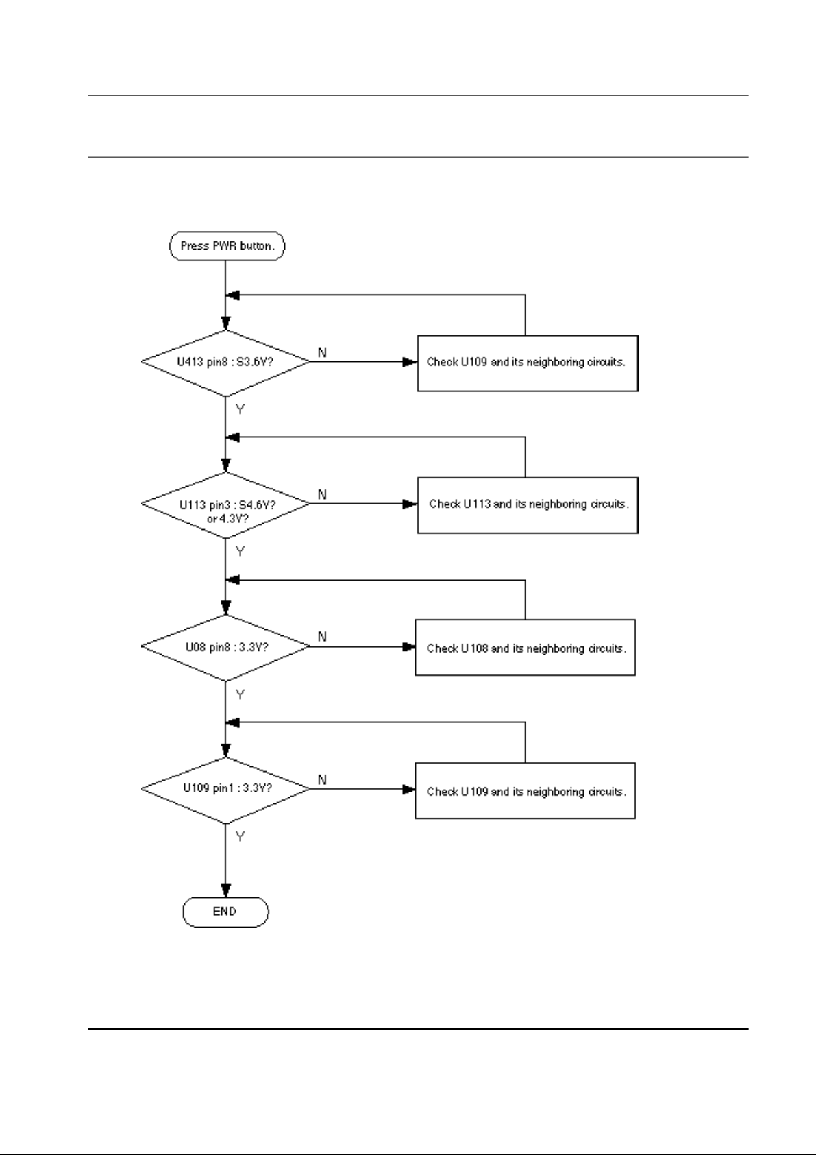
6-1-1 No Power
Samsung Electronics 6-1
Troubleshooting
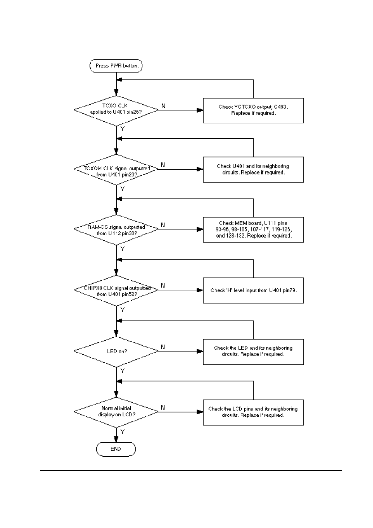
6-1-2 Abnormal Initial Operation (Normal +3.3 voltage source)
6-2 Samsung Electronics
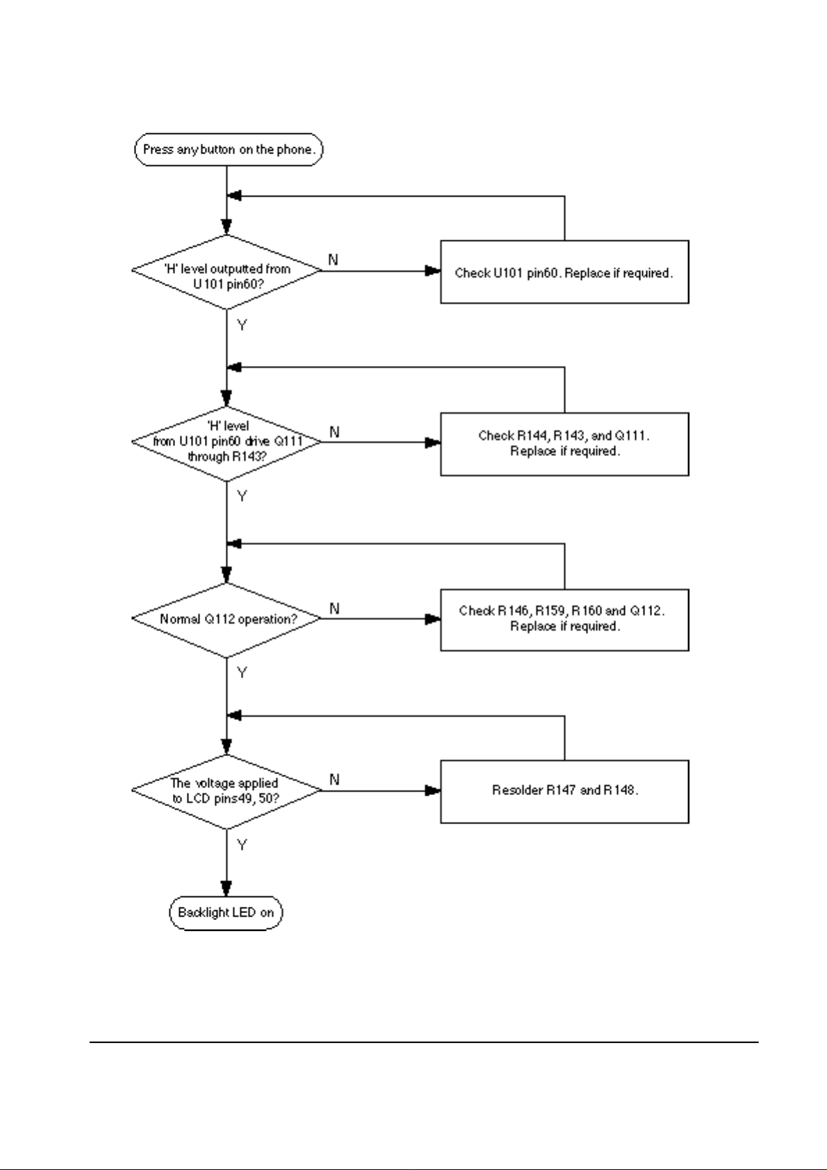
6-1-3 Abnormal Backlight Operation
Troubleshooting
Samsung Electronics 6-3
Troubleshooting
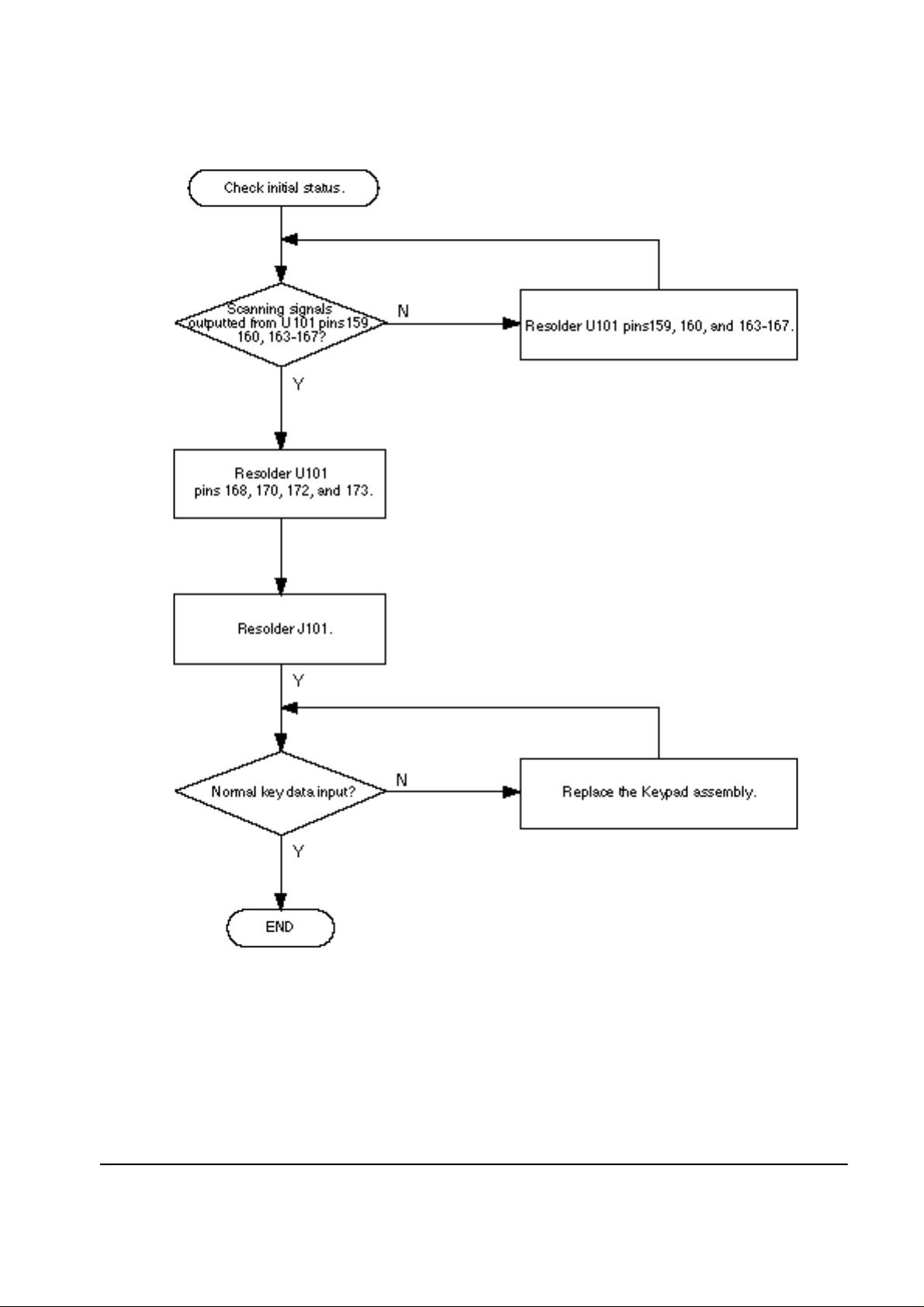
6-1-4 Abnormal Key Data Input
6-4 Samsung Electronics
 Loading...