

Samsung SCH-1000 Service Manual
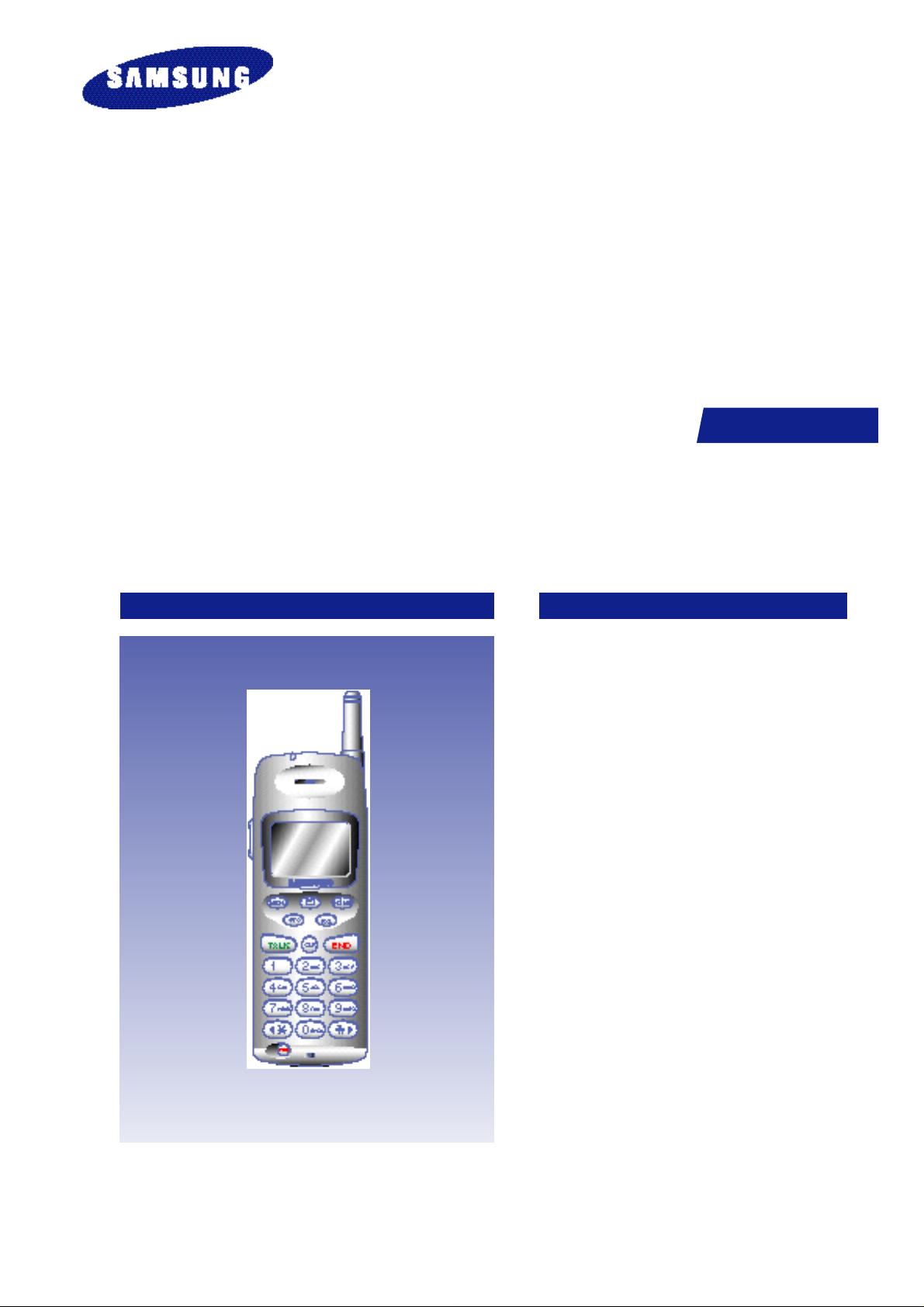
C D M A P O R TA B L E
Manual
PCS T E L E P H O N E
SCH-1000
S E RVICE
CDMA PORTABLE PCS TELEPHONE
CONTENTS
1. Specification
2. Installation
3. NAM Programming
4. Circuit Description
5. Test Procedure
6. Troubleshooting
7. Exploded Views and Parts List
8. PCB Diagrams
9. Electrical Parts List
10. Block & Circuit Diagrams

Samsung Electronics Co.,Ltd.
GH68-60563A
Printed in Korea.

1. Specification
1-1 General
Frequency Range
Transmitter : 1850 ° ≠1910 MHz
Receiver : 1930 ° ≠1990 MHz
Channel Bandwidth : 1.23 MHz
Channel Spacing : 50 KHz
Number of Channels : 1200
Duplex Separation : 80 MHz
Type of Emission : G7W
Input/Output Impedance : 50 ohms
Intermediate Frequency
Transmitter : 130.38 MHz
Receiver : 85.38 MHz
Local Frequency
Transmitter : 1st(FTX-130.38), 2nd(260.76MHz)
Receiver : 1st(FRX+85.38), 2nd(170.76MHz)
TCXO Frequency : 19.68 MHz
Frequency Stability : (FRX - 80MHz) °æ 150Hz
Operating Temperature : -30°… ° ≠+60°…
Supply Voltage : +4.8V
Current Consumption (Average)
Standby : 140mA (Non-slot mode)
Talk : 330mA (at +10dBm)
Size and Weight
Including Standard Battery : 146(H)°ø54(W)°ø25(D), 220g
Including Extended Battery : 146(H)°ø54(W)°ø33.5(D), 250g
Samsung Electronics 1-1

Specification
1-2 Transmitter
Waveform Quality : 0.944 or more
Open Loop Power Control Range
-25 dBm : -60.5dBm ° ≠-41.5dBm
-65 dBm : -20.5dBm ° ≠-1.5dBm
-104dBm : +15.0dBm ° ≠+30.0dBm
Minimum Tx Power Control : -50dBm below
Closed Loop Power Control Range : °æ24dB
Maximum RF Output Power : 200mW(+23dBm)
Occupied Bandwidth : 1.23MHz
Conducted Spurious Emissions @1.25MHz : -42 dBc/30KHz
1-3 Receiver
Rx Sensitivity and Dynamic Range : -104dBm, FER=0.5% or less
(Rate Set 1) : -25 dBm, FER=0.5% or less
Conducted Spurious Emission
1930 ° ≠1990 MHz : <-81dBm
1850 ° ≠1910 MHz : <-61dBm
All Other Frequencies : <-47dBm
Single Tone Desensitization : lower than 1%
Rx power=-101dBm
Tone power=-30dBm
Tone offset from carrier=°æ1.25MHz
Intermodulation Spurious Response Attenuation : lower than 1%
Rx power=-101dBm
Tone power 1=-43dBm
Tone power 2=-43dBm
Tone 1 offset from carrier=°æ1.25MHz
Tone 2 offset from carrier=°æ2.05MHz
1-2 Samsung Electronics
2. Installation
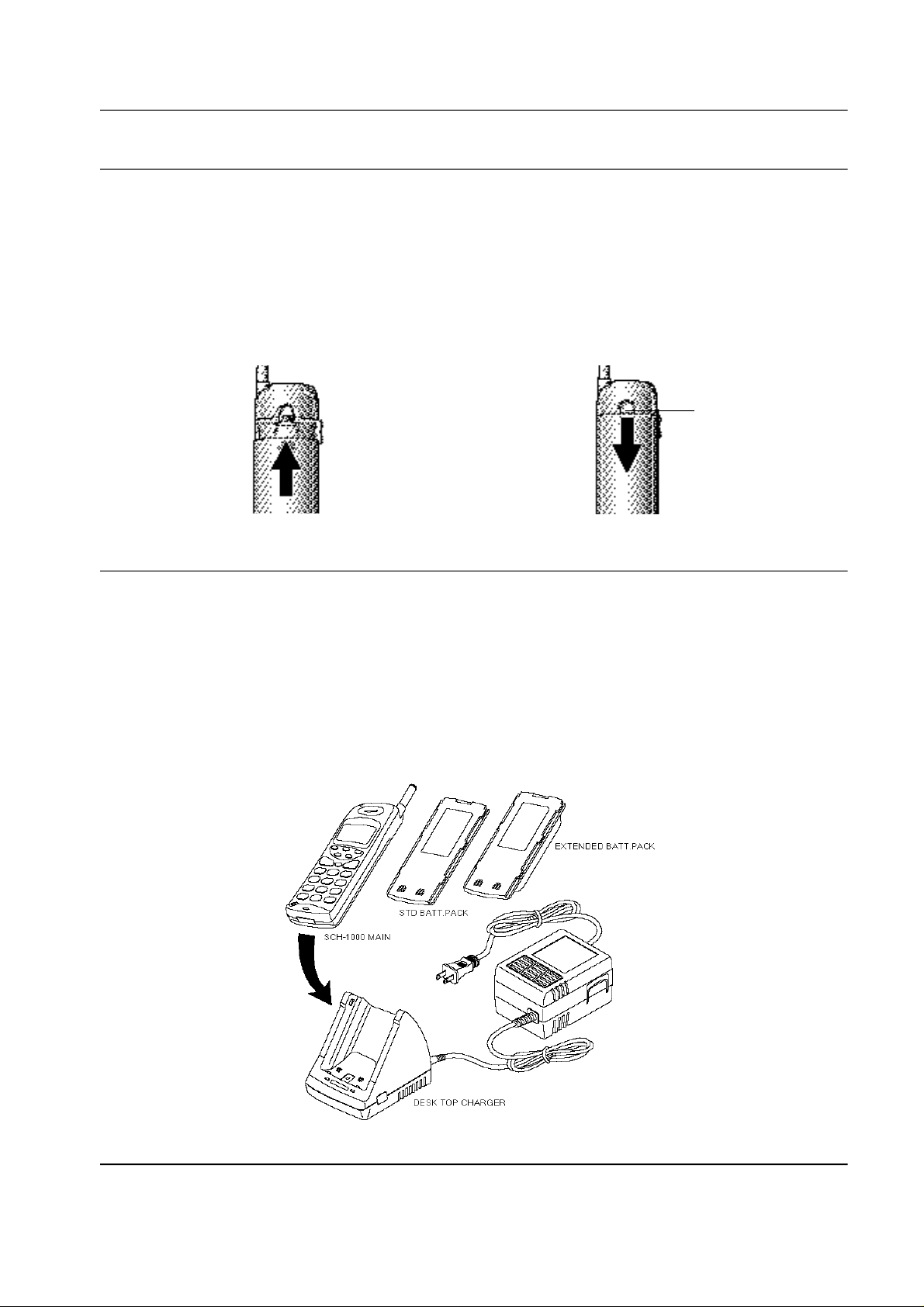
2-1 Installing a Battery Pack
1. To attach the battery pack after charging, align
it with the phone about 1cm (1/2") away from
its place so that the two arrows on the phone
are seen, the battery charge contacts pointing
downwards.
2. Slide the battery pack upwards until it clicks
firmly into position. The phone is now ready
to be turned on.
2-2 For Desk Top Use
1. Choose a proper location to install the charger
for desk top use.
2. Plug the power cord of the charger into an
appropriate wall socket. When the power cord
is connected correctly, the lamps turn on
briefly.
3. To remove the battery pack, release it by
pressing the button on the rear of the phone.
4. Slide the battery pack downwards about 1cm
(1/2") and lift it away from the phone.
Press this button to release
the battery pack
3. To charge the battery pack, insert the battery
pack into the rear slot of the charger. The lamp
marked BAT on the front panel of the charger
lights up red.
4. If you do not wish to use the phone while
charging the battery, insert the phone with the
battery pack attached into the front slot of the
charger. The lamp marked PHONE on the
front panel of the charger lights up red.
Figure 2-1 Charging The Phone and Battery
Samsung Electronics 2-1
Installation
2-3 For Mobile Mount
2-3-1 Antenna
1. Choose a proper location to install the
antenna.
¶UThe center of the roof top provides the best
performance.
¶UThe edge of the rear trunk also provides a
good performance. However, the antenna
should be higher than the roof of the car.
¶UIn case of on-glass antenna, you should
align the antenna base with the round plate
to connect the cables correctly.
2. Mount the antenna vertically, connect the
antenna cable.
3. Tighten the antenna nut fully.
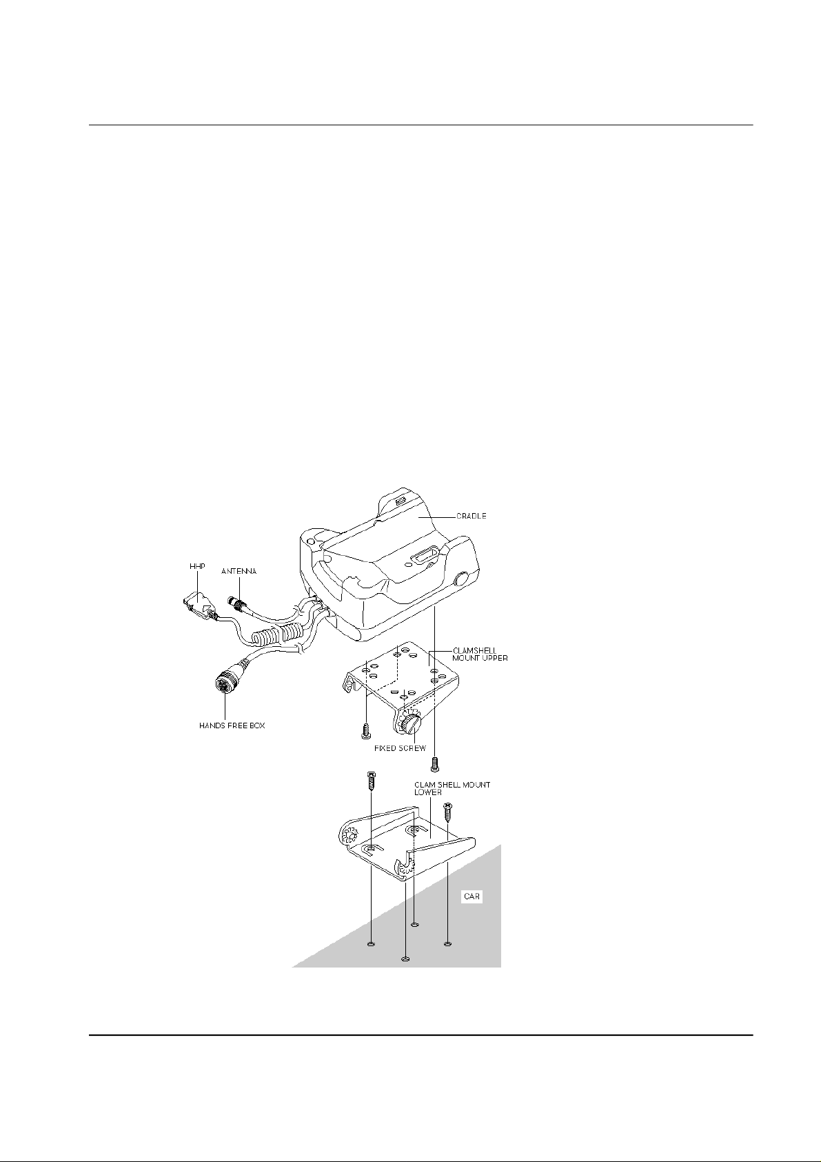
2-3-2 Cradle
1. Choose a location where it is easy to reach and
does not interfere with the driver's safe
operation of the car.
2. Separate the two halves of the clamshell by
removing the two large slotted screws. See the
figure 2-2.
3. Drill holes and mount the lower half of the
clamshell by using the screws.
4. Place the cradle onto the remaining half of the
clamshell and assemble them by using the
screws.
5. Reassemble the two halves of the clamshell
together. Adjust the mounting angle and
tighten the two slotted screws.
Figure 2-2 Cradle Installation
2-2 Samsung Electronics
Installation
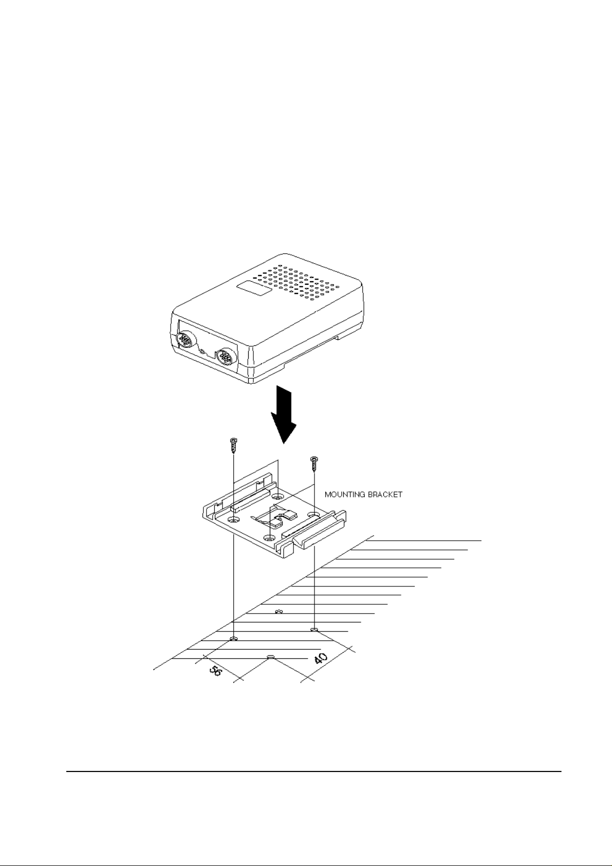
2-3-3 Hands-Free Box
1. Drill holes in a proper location for the handsfree box, attach the mounting bracket by using
the screws. See the figure 2-3.
2. Install the hands-free box into the bracket.
2-3-4 Hands-Free Microphone
1. It is recommended to install the microphone
where it is 30-45 cm (12-18") away from the
driver. Choose the location where is least
susceptible to interference caused by external
noise sources, ie, adjacent windows, radio
speakers, etc. Normal place is the sun visor.
2. Once the microphone has been correctly
positioned, connect the microphone wire to
the MIC jack on the hands-free box.
Figure 2-3 Hands-Free Box Installation
Samsung Electronics 2-3
Installation
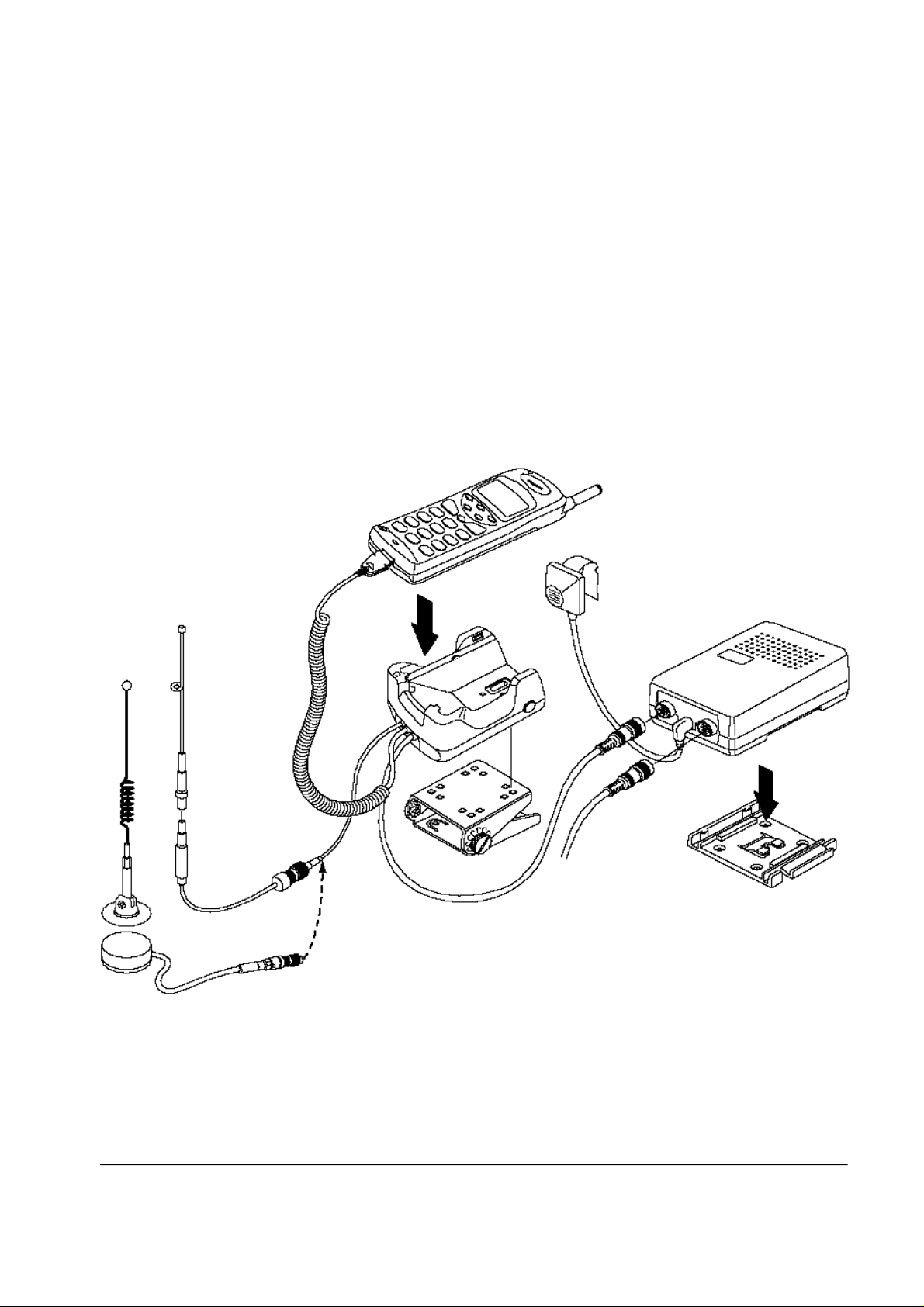
2-3-5 Cables
1. Connect the cradle and the hands-free box
with the data cable. See the figure 2-4.
2. Connect the antenna cable to the RF jack of the
cradle.
3. Connect one end of the power cable to the
battery or ignition terminal. Connect the red
wire to the battery (+) terminal, black wire to
the vehicle chassis. Then connect the battery (-)
terminal to the vehicle chassis.
4. Connect the other end of the power cable to
the PWR jack of the hands-free box.
Notes:
¶UIt is recommended to connect the power cable
directly to the battery to avoid power noise.
¶UMake sure the connection between the battery -
terminal and the vehicle chassis is made
correctly.
¶UMake sure the fuse having a proper capacity is
used on the power cable.
¶UMake sure the cables do not pass over any sharp
metal edge that may damage it.
Figure 2-4 Cable Connections
2-4 Samsung Electronics

3. NAM Programming
NAM features can be programmed as follows:
Notes:
-If you enter the NAM program mode, each item shows the currently stored data. Go to the next item by
pressing STO.
-You can modify the data by entering a new data.
-If you enter a wrong digit, press CLR to delete the last digit. Press and hold CLR to delete all digits.
-To scroll items backwards or forwards, press the VOLUME button on the left side of the phone.
3-1 General Setup
LCD Display Key in Function
MENU, 5, 0 -selects NAM programming
Enter Lock
??????
SVC Menu°Ë°È
1:PCS Phone#
2:General
ESN
B0000000
CAI version
VOC13K/8K
SO_VOICE_13K
SCM
00001010
Lock Code
0000
Slot Mode
No
6-digit code -Enter random 6-digit code (MSL)
2 -choose 'GENERAL.'
Volume °„ -Electronic Serial Number of the phone is displayed
Volume °„ -Common Air Interface version is displayed
1
°Ëor°È -Select vocoder service option
STO -stores it
Volume °„ -Station Class Mark displays the power class,
transmission, slotted class, dual mode.
Lock code, current status is displayed
4-digit code -to change, enter new code.
STO -stores it.
Slot mode. 'Yes' indicates the slot mode.
°Ëor°È -changes the status.
STO -stores it.
Slot Index
2
Samsung Electronics 3-1
0 - 7 -to change, enter new one.
STO -stores it.
Slot mode index. The higher, the longer sleeping time.

NAM Programming
3-2 Setting Up NAM
LCD Display Key in Function
SVC Menu°Ë°È
1:PCS Phone #
2:General
Volume °„ -NAM Programming Menu is displayed
SVC Menu°Ë°È
3:NAM
IMSI_MCC
310
IMSI_MNC
00
CDMA ACCOLC
CDMA HomeSID
Yes
CDMA fSID
Yes
CDMA fNID
Yes
3 -choose 'Setup NAM'
number IMSI Mobile Country Code, current code is displayed.
STO -to change, enter new one.
-stores it.
number IMSI Mobile Network Code, current code is displayed.
STO -to change, enter new one.
-stores it.
CDMA Access Over load Class, current status is displayed.
0
class number -to change, enter new one.
STO -stores it.
CDMA Home system ID, current status is displayed.
°Ëor°È -changes the status.
STO -stores it.
CDMA foreign SID, current status is displayed.
°Ëor°È -changes the status.
STO -stores it.
CDMA foreign NID, current status is displayed.
°Ëor°È -changes the system.
STO -stores it.
SID
4120
NID
65535
3-2 Samsung Electronics
number -to change, enter new one.
STO -stores it.
number -to change, enter new one.
STO -stores it.
first SID written in the list, current status is displayed.
first NID written in the list, current status is displayed.

4. Circuit Description
4-1 Logic Section
4-1-1 Power Supply
With the battery installed on the phone and by
pressing the PWR key, the VBATT and ON_SW
signals will be connected. This will turn on
Q108(2SC4081). This in turn will be supplied to
pin 6 of regulators U110 and U111, thus releasing
them from the shut-down state to output
regulated 3.3V. And then Reset Generator (U109)
stays High.
The VBATT applied to ON_SW turns on
Q113(DTC144) and will result in the signal
ON_SW_SENSE to change state from HIGH to
LOW. The MSM recognizes this signal and sends
out PS_HOLD(logical HIGH) to turn on
Q108 even after the PWR key is released.
The power from U110 is used in the digital part of
MSM and BBA. The power from U111 is used in
the analog part of BBA.
4-1-2 Logic Part
The Logic part consists of internal CPU of MSM,
RAM, ROM and EEPROM. The MSM receives
TCXO and CHIPX8 clock signals from the BBA
and controls the phone. The major components are
as follows:
¶UCPU : INTEL 80186 core
¶UFROM : U112 (LH28 F800SUHE)-8MBIT
FLASH ROM
¶USRAM : U113(KM68V1000BLTI)-1MBIT
STATIC RAM
¶UEEPROM : U107(24LC65-1/SM)-64KBIT
SERIAL EEPROM
CPU
INTEL 80186 CMOS type 16-bit microprocessor is
used and CPU controls all the circuitry. For the
CPU clock, 27MHz is used.
FLASH ROM
One 8Mbit FROM is used to store the terminal's
program. Using the down-loading program, the
program can be changed even after the terminal is
fully assembled.
SRAM
Two 1Mbit SRAMs are used to store the internal
flag information, call processing data, and time
data.
EEPROM
One 64Kbit EEPROM is used to store ESN, NAM,
power level, volume level, and telephone number.
KEY-PAD
For key recognition, key matrix is setup using
SCAN0-6 of STROBE signals and KEY0-3 of input
ports of MSM. Eight LEDs and backlight circuitry
are included in the keypad for easy operation in
the dark.
LCD MODULE
LCD module contains a controller which will
display the information onto the LCD by 8-bit data
from the MSM. It also consists a DC-DC converter
to supply -3.3V for fine view angle and LCD
reflector to improve the display efficiency.
Samsung Electronics 4-1

Circuit Description
4-1-3 Base Band
MOBILE SYSTEM MODEM (MSM)
The MSM equipped with the INTEL 80186 CPU
core is an important component of the CDMA
cellular phone. The MSM comes in a 176 pins
TQFP package. The interface block diagram is
shown on page4-3.
MICROPROCESSOR INTERFACE
The interface circuitry consists of reset circuit,
address bus (A0-A19), data bus (AD0-AD15), and
memory controls (ALE,DT-R,HWR/,LWR/,
RAM_CS/,ROM_CS).
INPUT CLOCK
°§CPU clock : 27 MHz
°§TXCO/4 (pin34) : 4.92 MHz. This clock signal
from the BBA is the reference clock for the MSM
except in CDMA mode.
°§CHIPX8 : 9.8304 MHz.The reference clock used
during the CDMA mode.
ADC Interface
ADC_CLK (pin3), ADC_ENABLE (pin1) and
ADC_DATA (pin2) are required to control the
internal ADC in the BBA.
Data Port Interface
Includes the UART. Also, supports Diagnostic
Monitor (DM) and HP equipment Interface.
CODEC Interface
The MSM outputs 2.048MHz PCM_CLK (pin19)
and 8KHz CODEC_SYNC (pin16,20) to the
CODEC (U102). The voice PCM data from the
MSM (U101)PCM_DIN (pin135) is compressed
into 13KHz by PureVoice algorithm in the CDMA
mode.
RF Interface
BBA INTERFACE
CDMA,Data Interface
°§TXIQDATA0-7 (pin24-32) : TX data bus used
during both CDMA.
°§C_RX_IDATA0-3 (pins16-20) and
C_RX_QDATA0-3(pins 12-15) : RX data bus
used during CDMA mode.
Clock
°§TX_CLK(pin 22), TX_CLK/(pin23) : Digital to
Analog Converter(DAC) reference clock used in
TX mode.
°§CHIPX8 : ADC reference clock used in CDMA
RX mode.
TX : TX_AGC_ADJ (pin35) port is used to control
the TX power level and PA_ON (pin44) signal is
used to control the power amplifier.
RX : AGC_REF (pin36) port is used to control the
RX gain and TRK_LO_ADJ (pin45) is used to
compensate the TCXO clock.
General Purpose I/O Register Pins
Input/output ports to control external devices.
Power Down Control
When the IDLE/signal turns LOW, only the TX
sections will be disabled.If both the IDLE/ and
SLEEP/ are changed to LOW, all the pins except
for the TXCO are disabled.
4-2 Samsung Electronics
Circuit Description
Figure 4-1 Baseband Block Diagram
4-1-4 Audio Section
TX AUDIO PATH
The voice signal output from microphone is
filtered and amplified by the internal OP-AMP
and is converted to PCM data by the
CODEC(U102). This signal is then applied to the
MSM(U101)'s internal vocoder.
RX AUDIO PATH
The PCM data from the MSM are converted to
audio signal by DAC of CODEC(U102),is then
amplified by the speaker amplifer(U105) to be sent
to the speaker unit.
VOLUME ADJUST
Volume can be adjusted up to 8 steps for the user
to obtain a proper loudness of received signal.
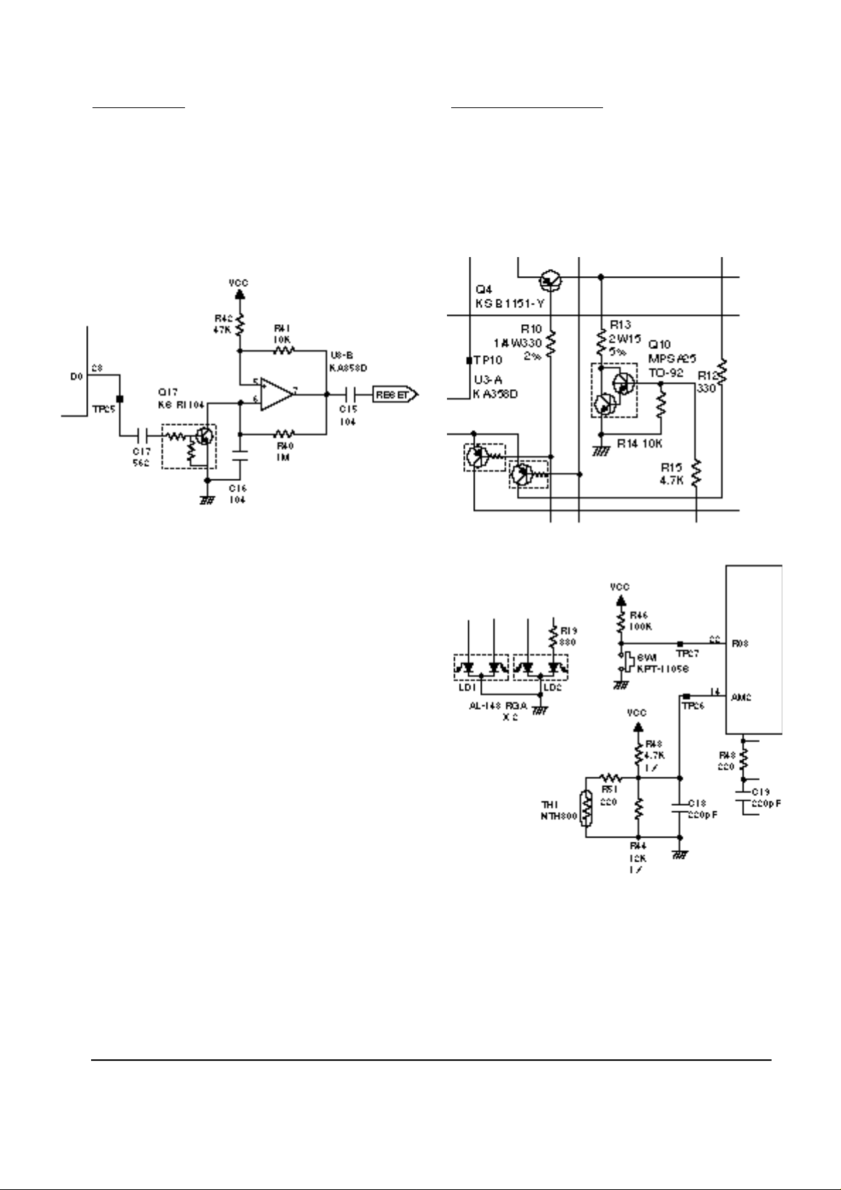
4-1-5 Buzzer Driving Circuitry
Buzzer generates alert tone. When the buzzer
receives the timer signal from the MSM, it
generates alert tone. The buzzer level is adjusted
by the alert signal's period generated from the
MSM timer.
4-1-6 Key Tone Generator
Ring signal (pin49) from MSM(U101) is passed
through LPF consisting of R180, C119, R124, and
C120, amplified at the speaker amp(U105) and
come out to speaker.
Samsung Electronics 4-3

Circuit Description
4-2 Receiver Section
LOW NOISE AMPLIFIER (LNA)
The low noise amplifier featuring 1.6dB Noise
Figure and 19dB gain amplifies a weak signal
received from the base station to obtain the
optimum signal level.
DOWN CONVERTER (MIXER)
First local signal is applied to this down converter.
The down converter transfers the signal amplified
at the LNA into 85.38 MHz IF signal. 85.38MHz IF
signal is made by subtracting 1960°æ30MHz RF
signal from 2045.38°æ30MHz first local signal. The
LNA is Q303 and down converter is U302.
IF AMP
The IF amp (Q310) amplifies the output signal of
the down converter (U302).
RF IF AUTOMATIC GAIN CONTROLLER
(AGC) AMP
85.38 MHz IF signal is applied to IF AGC amp,the
AGC output level is applied to BBA (Base Band
Asic). The AGC amp (U303) keeps the signal at a
constant level by controlling the gain. Dynamic
range is 90dB, up gain +45dB, and down gain 45dB.
RF BAND PASS FILTER (BPF)
The RF BPF(F302) accepts only a specific
frequency (1960°æ30MHz) from the signal
received from the mobile station. The bandwidth
is 60MHz.
BUFFER
Buffer (Q311) amplifies the signal from the VCO
(U305) to be applied to the local input of the down
converter (U302) when a phase is locked between
U304 and U305.
The VCO (U305) generates the signal having
2045MHz center frequency and °æ30MHz
deviation with the voltage control. PLL IC(U304)
controls this signal.
PHASE LOCKED LOOP (PLL)
Input reference frequency is generated at
VCTCXO (U306) and the local signal is generated
at VCO. PLL compares the two signals and allows
the VCO controlled by voltage to generate the
desired signal with pre-programmed counter.
VOLTAGE CONTROLLED TEMPERATURE
COMPENSATED CRYSTAL OSCILLATOR
It provides 19.68MHz reference frequency to PLL
(U304,U402) and BBA (U401). A correct frequency
tuning is made by the voltage control.
DUPLEXER
Duplexer (F301) controls to transmit through the
antenna only the signals within acceptable Tx
frequency range (1880°æ30MHz) and to receive
through the antenna only the signals within
acceptable Rx frequency range (1960°æ30MHz). It
also matches LNA(Q303) input in receiving part
and PA output in transmitter part with the
antenna.
IF SAW BAND PASS FILTER FOR CDMA
IF SAW BPF (F303) is used for CDMA system
having 1.23 MHz wide band and °æ630kHz band
width. The filter also climinates the image product
generated at the mixer.
4-4 Samsung Electronics

4-3 Transmitter Section
Circuit Description
POWER AMP MMIC
Power Amp MMIC (U407) amplifies signal to be
sent out to the base station through the antenna.
DRIVER AMP
The driver amp (Q411,Q413) allows the input
signal to the power amp MMIC(U407) to be within
a specified level.
UP CONVERTER (MIXER)
The up-converter (U405) receives the first local
signal to generate 1880°æ30MHz from the signal
controlled by TX AGC amp (U404). 1880°æ30MHz
signal comes out of the mixer output by adding
130.38MHz IF signal to 1749.62°æ30MHz first local
signal. The driver amp's reference number is Q411,
Q413 and up converter's reference number is U404.
IF AUTOMATIC GAIN CONTROLLER AMP
ANTENNA
ANT1 allows signals to send and to receive to
from the base station.
RF BAND PASS FILTER (BPF)
The RF BPF (F402) accepts only a specific
frequency (1880°æ30MHz) to send it out to power
amp MMIC. The bandwidth is 60MHz.
POWER SUPPLY SWITCHING
Power supply switching (Q412) turns on TX
POWER when the phone is in traffic mode and
supplies power to the circuits.
ISOLATOR
Isolator (I401) is used to reduce a reflected signal
to protect the power amp MMIC from being
damaged.
The signal output from BBA (Base Band ASIC)
should be a constant level. The TX IF AGC amp
(U404) controls power to keep the signal at a
desired level. Dynamic range is 85 dB, up gain
+40dB, and down gain -45dB.
POWER SUPPLY REGULATOR
The power supply regulator (U414) generates the
regulated power.
POWER SUPPLY REGULATOR
The power supply regulator (U413,U414) supplies
a regulated power to each part of transmitter.
U413 supplies 4.8V to Tx driver (Q411,Q413) and
Power Amp MMIC (U407). U414 supplies 4.2V to
the others.
Samsung Electronics 4-5

Circuit Description
4-4 Hands-Free Kit
Hands free board is largely composed of car
adapter circuit and Hands free circuit.
4-4-1 Car Adapter Circuit
POWER SUPPLY
Input power switching circuit : This circuit
includes Short protection circuit, and Power
switching control circuit. It supplies power for
HHP and hands free kit.
+13.5V switching circuit (Q801, 802) : This circuit
switches power for power amplifier using MPU
mute signal.
HHP power circuit : This circuit is Switching
regulator. Input voltage is +13.6v, output voltage
is +5.8v.
Voltage detection circuit : Charging circuit is
designed to stop charging when the voltage of
battery is dropped.
The voltage of battery is entered to A/D converter
located in U703 #2.
Temperature detection circuit : The temperature
of battery is measured by missing NTC thermistor.
NTC themistor has a characteristics of Log-scale. It
obtains a linear characteristics by the parallel
connection of resistors.
4-4-2 Hands Free Circuit
POWER SUPPLY (U704,U808)
+5V is regulated by U704 for hands free circuit,
and -5V is regulated by U808.
TX PATH
Vcc regulator (U704) : This circuit regulates Vcc
(+5V).
CHARGER CIRCUIT
This circuit charges battery pack by detecting the
temperature of battery, the slope of temperature,
the slope of the voltage of battery, and charging
time, etc.
During charging, the charger LED turn on red.
When charging is completed, the charger LED
turns on green.
Battery Type Capacity Charge Current Charge Voltage
S t a n d a r d 8 5 0 m A H 3 0 0 m A 6 . 2 V
E x t e n d e d 1 5 0 0 m A H 6 0 0 m A 6 . 7 V
The audio signal from external mic(JP705) flows
into U802 pin #11. U802 includes Amplifier and
Control circuit for hands free operatin. U801A
amplifies input signal. Output signal is
transmitted to HHP.
RX PATH
Input audio signal cancels noise by difference
amplifier (U801c). U802 performs hands free
action. The RX audio signal is input (U805). The
speaker drive amp (U804) amplifies the Rx audio
signal and the output of U804 goes out of speaker.
4-6 Samsung Electronics
4-5 Desk-Top Rapid Charger
4-5-1 Description
Circuit Description
The following document will provide the
specifications for SAMSUNG-SPRINT's battery
charger unit, system #PCS, which be sold as an
accessory to cellular telephone, model SCH1000/RC.
Two bi-color LED indicate charging status of each
battery type. Charging current is automatically
controlled and battery type is indentified by the
resistance between BATT_R(RR) and GND(B–)
contact of battery.
The bettery charger sequentially charges two
NiMH batteries that are to be used with the
cellular telephone.
The first slot will be able to accommodate a battery
4-5-2 Specification
attached to the cellular telephone. The second slot
can be used a spare battery.
This specification is applied to every unit of
PCS/RC, revision level 0.
This charger supports several types of protection
mode and intelligent algorithem to cope with
abnormal cheminal reaction, early cut-off,
excessive temperature, battery short/open, etc.
4-5-3 Interface Requirements
I/O DESCRIPTIONS
The interface requirements for the charger base will consist of the following signals.
Wall Adaptor Interface
Signal Technology Type Description From/To
+13V Analog I Supply Voltage Wall Adaptor
Battery Interface
Signal Technology Type Description From/To
BATT1+ Analog I/O Positive Conductor B a t t e r y 1
BATT1- Analog I/O Negative Conductor B a t t e r y 1
NTC1 Analog I Thermistor Input B a t t e r y 1
RR1 Analog I Type Check B a t t e r y 1
BATT2+ Analog I/O Positive Conductor B a t t e r y 2
BATT2- Analog I/O Negative Conductor B a t t e r y 2
NTC2 Analog I Thermistor Input B a t t e r y 2
RR2 Analog I Type Check B a t t e r y 2
Samsung Electronics 4-7

Circuit Description
BATTERY CHARGING CURRENT
• EXTENDED BATTERY : 900mA °æ 10%
• STANDARD BATTERY : 630mA °æ 10%
BATTERY DISCHARGING CURRENT
• 200~350mA
ENVIRONMENT SPECIFICATION
• Temperature
Operating 0 to 45oC
Storage -25 to 85oC
• Humidity 10 to 90%
• Atospheric pressure 6.5 x 10⁴to 1.05x 10⁵Pascals
BATTERY INDENTIFICATION
• EXTENDED BATTERY : 330 OHM resistance
between RR and B–
• STANDARD BATTERY : 680 OHM resistance
between RR and B–
LED INDICATION
• DC POWER ON : Instantaneous YELLOW
flickering of both LED.
• SLOT INDENTIFICATION
LED 'LEFT' : FRONT SLOT (PHONE)
LED 'RIGHT' : REAR SLOT (BATT)
• CHARGING STATUS
RED : CHARGING
GREEN : CHARGING TERMINATION (Full
Charge)
YELLOW : LOW BATTERY (WAIT)
FLASHING YELLOW : DISCHARGING
FLASHING R °Ê G °Ê Y, FLASHING RED :
Hardware Error.
OFF : BATTERY UNLODED, etc...
MECHANICAL SPECIFICATION
• The cahrge unit will be enclosed within a plastic
housing that is terminated on one end by a DC
wall adapter.
• Dimensions
CASE MATERIAL : POLY CARBONATE
(LEXAN 940)
COLOR : BLACK
WEIGHT : About 300g
4-8 Samsung Electronics
Circuit Description
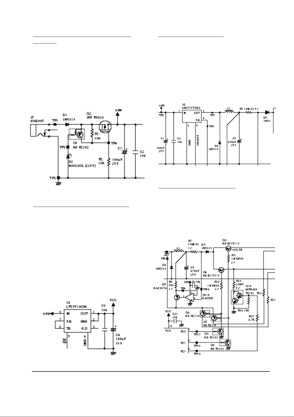
PROTECTION CIRCUIT FOR EXCESSIVE
VOLTAGE
The norminal voltage of Zener diode D2 is 22V
and the reverse voltage by leakage current is about
14.5V.
If the input voltage is under 22V, the Q1 stays off
and the gate of FET Q2 becomes low level and
turns on main path. If the voltage is higher than
22V or excessive impulsive voltage is supplied, D2
becomes breakdown and turns on Q1 and turns off
Q2 by raising the gate voltage to high level.
STEP-DOWN REGULATOR
The step-down buck converter is composed of U2
(LM2576T-ADJ), L1, D4 and C6. And U2 choppers
the output by switching operation in 52 kHz
internally fixed frequency. Pin 5 is connected to
pin 3 of MPU and becomes on/off and controls the
output voltage by adding/subtracting the
feedback voltage of pin 4. D4 is a diode to
flywheel the energy of L1 when the switching TR
of Buck circuit is off.
MICROPOWER VOLTAGE REGULATOR
When power is on and off, pin 5 of U1 (LP2951)
detects the output voltage and keeps high/low
level and the reset pin 18 of MPU becomes active
by the voltage level of pin 5.
The error flag becomes high impedance state at the
input voltage of under 1.3V and changes the state
to low level when the voltage reaches to 5V and
then resets MPU. Also the error flag becomes low
state at the output voltage of under 4.75V and
resets MPU.
By this way MPU can keep the input voltage of
CMOS or TTL device stable and prevents
malfunctions.
CONSTANT CURRENT CIRCUIT
As the constant current circuit which is adapted
with PCS/RC, is just one directional, it can be
used as power source of OP-amp.
By applying and fixing input bias current to N.1
terminal of U3, the sink current is controlled by
shunt resistor R7, R8, R12 and RR of the battery
pack.
Samsung Electronics 4-9

Circuit Description
CHARGE MAIN PATH
MPU turns on Q8 or Q9 with high level output
from pin 2 for front port and pin 1 for rear port.
Q8 and Q9 pull down the base voltage level of
PNP TRQ3 and Q4. It turns on main path, then
charging is started.
BATTERY TEMPERATURE DETECTION
The temperature of the battery pack in the front
port and rear port is detected by R36/R37 and
R34/R35, respectively, and measured as A/D
value at MPU pin 15.
Analog switch U5 selects 2 channels (CH1 : pin 6,
CH2 : pin 7) sequentially by the Enable Pulse of
MPU pin 19 and assigns the NTC voltage of the
front and rear batteries to pin 1 of U5.
DETECTION OF CHARGE VOLTAGE
The battery voltage of front port is divided by R28,
R30 and R32, measured as A/D value by MPU pin
12 through OP-amp. And the battery voltage of
rear port is divided by R29, R31 and R33, and
measured as A/D value by MPU pin 13.
MONITORING AMBIENT TEMPERATURE
Ambient temperature is detected by R43 and
R44/R61+TH1 and measured by MPU pin 14.
As the temperature is very important, it is
constantly checked once program is started.
4-10 Samsung Electronics
Circuit Description
WATCH DOG
It is possible that battery is overcharged if charger
stops operation by keeping on charging port by
external impact.
To avoid it, timer (U3-B) is prepared and MPU is
forced to be reset if MPU dosen't clear timer until a
specified time is elapsed.
DISCHARGE CIRCUIT
Discharging battery is available in the rear port
and initiated once pin 22 of MPU acknowledges
the depression of discharge switch.
Discharging is controlled by pin 6 of MPU and
stops operation once the voltage is reached to
1V/cell and automatically starts charging routine.
Samsung Electronics 4-11
Circuit Description
4-6 Cigarette Lighter Adapter
4-6-1 Funtional Specification
SUMMARY
This standard describes on the specifications of
CLA(Cigarette Lighter Adaptor) for the SCH-1000
of SAMSUNG.
CLA AS ADAPTOR AND CHARGER
¶UAdaptor
directly supplies power in order to operate
cellular phone independent of the battery pack.
¶UCharger
for the NiMH battery pack
ELECTRICAL SPECIFICATION
¶UInput Voltage : 11V to 16.5V DC
(normal voltage : 13.5V DC)
¶UOutput Current
- HHP POWER : supplies 100mA if cellular
phone mode is in stand_by state and 300mA
to 600mA in carrier_on state.
- Battery Charge Current : 390mA +/- 10%
(carrier_off) 10ßðæ1 0ßÃ(carrier_on, full_charge)
FUNCTIONS OF CLA
¶UProtection Circuit
Protection Circuit is the circuit against the
electrical stress which is occured at
unexpected conditions of the source power of
CLA unit such as reverse voltage or overcurrent.
¶UDetection of cellular phone
If cellular phone is connected to CLA, the
CLA lamp is on to display whether charge
will be done normaly or not.
¶UDetect Carrier-On
In the case of Carrier-On, CLA detects the
resistance of the Cellular Phone and reduces
the charge current.
¶UDetect Full-Charge
If the temperature of the battery pack is
higher than the temperature outside of the
cellular phone, CLA detects the battery fully
charged and the state will be converted to the
Trickle Charge.
CLA CURL CABLE CONNECTION
¶UOutput Voltage (when 2K•ÿ is loaded to the
battery charge terminal)
- Battery Charge Terminal : 5.8°æ0.5V
- HHP POWER Terminal : 5.8V(+/- 0.3V)
¶URipple & Noise : 50mVp-p
¶UNormal Fuse Capacity : 250V, 2A
¶UCharge Time : 3Hrs. at 850mAh6Hrs. at
1500mAh
ENVIRONMENTAL SPECIFICATION
¶UTemperature
- Operating Temperature : 0°… to 50°…
- Storage Temperature : -20°… to 85°…
¶UHumidity
- Operating Humidity : 5% to 90%
- Storage Humidity : 5% to 95%
PIN NO(CLC) Description PIN NO(HHP)
#1 HHp Power 12 or 13
#2 BATT 16
#3 Thermistor 15
#4 C/F 3
#5 GND 2 or 4 or 6
4-12 Samsung Electronics

4-6-2 Schematic Description
Circuit Description
DC-DC CONTROLLER
KA7500B(U1) is DC-DC Controller. It reads the
voltage difference between E1I+ Port and E1I- Port
and controls time to turn on Q1. E2I+ and E2Iturn on Q1 in the same way. U1 also supplies +5V
of Reference Voltage(Vref).
STATIC CURRENT
E1I- Port of U1 detects about 1.25V untill FullCharge and controls the TURN ON time of Q1 in
order to detect 1.25V at E1I+ Port. To make the
E1I+ Port detect 1.25V continuously, 0.19V of
voltage reduction will be generated on R4. At the
equation of V=I*R, the current of R4 is around
390mA and it will be the charge current.
BATTERY CHARGE CURRENT CUTTING BY
RELATIVE TEMPERATURE
Although every battery sample applied to the
SCH-1000 has almost the same battery
temperature at Full-Charge, it varies according to
the relative temperature.
So the battery temperature at Full-Charge may be
different according to the temperature around the
cellular phone.
PREVENT CHARGE CIRCUIT IN THE CASE
OF MOBILE PHONE CARRIER-ON
In the case of Mobile Phone carrier-on, the voltage
loaded on PIN-13 of U3D is lower than that of
PIN-12. So PIN-14 ouputs HIGH and Q3 is TURN
ON again. It results to the Prevent Charge.
LED-DRIVING CIRCUIT
When battery is inserted to CLC, the voltage
loaded to PIN-2 of U3A is lower than that of PIN-3
and PIN-1 outputs HIGH. This TURN ON Q7 and
drives LED.
If Full-Charge occures at 25°…, the voltage of U3C
to which the battery thermistor is connected is
around 2.11V and the voltage of the parallel
resistance of Th1 and R18 is about 2.11V. PIN 8 of
U3C will be HIGH and turn on Q3 if the
temperature is up. This generates the voltage
detected at E1I- of U1 around 0.1V and the charge
current reduces to 40mA. If Full-Charge occurs at
high temperature and low temperature, the battery
temperature varies and the voltage decline of Th1
and R18 relatively varies. So the battery FullCharge condition will be fulfilled.
Samsung Electronics 4-13

Circuit Description
4-7 Travel Charger
4-7-1 Description
This document defines the functional
requirements of SCH-110TC, SCH-1000TC,
designed as a Ni-MH battery charger for SCH-110,
SCH-1000.
This charger can be used with indoor AC input
directly.
One LED indicates charging status of battery.
Charging current mode is constant current mode
controled.
4-7-2 Scope
This specification is applied to every unit of model
no. SCH-110TC, SCH-1000TC, revision level 0.
-
EFFICIENCY : 50% min.
-
RIPPLE & NOISE
¶URIPPLE & NOISE LIMLT : 100mVp-p max.
¶UTEST CONDITION : At output contact with
20M Hz bandwidth using Battery load.
SAFETY REQUIREMENTS
-
UL1310 APPROVAL
-
FCC CLASS-B MEET
-
PRIMARY-SECONDARY ISOLATION
¶UWithstanding voltage : 150 Vac min for 1
minute or 1800 Vac min for 1 second.
¶UCut-Off Current : 10mA
4-7-3 Reference
REFER TO TEST PROCEDURE
4-7-4 Electrical Characteristic
AC INPUT
-
AC INPUT VOLTAGE : 120Vac nominal
-
AC INPUT VOLTAGE R A N G E : 90-140Vac
-
AC INPUT CURRENT: 0.3A max.
-
AC INPUT FREQUENCY : 60°æ3 Hz
OUTPUT
-
BATTERY CHARGING VOLTAGE : 4.8 ~ 8.0
VDC nominal
-
BATTERY CHARGING CURRENT RANGE
under C-C Mode : 350°æ20mA
-
CHARGING CURRENT SETTING : 350°æ
10mA with 120Vac input and 18•ÿ load
resistance.
-
BATTERY CHARGING CURRENT RANGE
under C-C MODE :
¶USTANDARD BATTERY : 350°æ20mA
¶UEXTENDED BATTERY : 350°æ20mA
BATTERY IDENTIFICATION
BATTERY
TYPE
EXTENDED BAT.
STANDARD BAT.
C H A R G I N G
C U R R E N T
C/F - GND
330•ÿ
or
680•ÿ
L O A D
R E S I S T A N C E
18•ÿ350 °æ 20mA
LED INDICATION
-
CHARGING STATUS
-
Red : Charging
ENVIRONMENTAL
-
UNIT OPERATING TEMPERATURE RANGE :
0 to 40 ° ∆C
-
STORAGE TEMPERATURE RANGE :
-10 to 70 ° ∆C
4-14 Samsung Electronics

4-7-5 Mechanical Specification
Circuit Description
-
CASE SIZE : 140.8mm°ø54.4mm°ø23.9mm
-
CASE MATERIAL : PC (LEXAN 940)
-
COLOR : BLACK
-
WEIGHT : 110g
4-7-6 Explanation Of Operating
BASIC CIRCUIT CONFIGURATION
Ttavel charger is consisted with power supply and
charging controller, And this charger is also
specified to input filter, rectifier, transformer,
secondary filter, feed-back circuit, battery charging
control circuit and LED display.
OPERATING IN EACH BLOCK
Input Filter, Rectifier
The AC power, which comes from AC-input line,
is changed to DC power by following through F1,
VA1, C01, LF1, D1, C03, C04.
(there are F1 for over current protection, VA1 for
input surge protection, C01, LF1 and C02 for
reducing noise, D01 for converting AC to DC. )
Feed Back Circuit
The transferred energy is rectified and flattened by
D20, C21 and C22.
The case of non-battery and off-state of Q20,
output voltage is regulated to 8VDC by feed back
sampling voltage divided by r27 and r28/r29.
U21 offers reference, compares this to sampling
voltage and send the difference to PWM control
circuit by OP1.
Battery Charging Control and LED Display
Circuit
In the case non-battery, LED is off state by being
on state of q24.
*refer to below table
U23
U24
OUT-A
L
OUT-B
H
L
q21 q20
OFF OFFL
When battery is inserted and the voltage of
comparator U23A Term.#3 is higher than the
voltage of Term.#2, LED is RED color by being
OFF of q24, and q21 is off because of U23A is 'L'
Switching Controller & Transformer
When DC power of 2.1 makes Q01 to turn-on by
biasing gate of it through r03 ~ r07, the current of
primary winding of T1 increases.
As a result, the energy of primary accessary
winding accelerates turn-on of Q01, and the pick
current of primary main winding makes q02 to
turn-on by converted voltage to R02. this result
reduces gate voltage of Q01, the current of
primary main winding consequently. this makes
reverse bias energy to gate of Q01, it is turn-off
quickly. The energy transfers to secondary
winding at that time.
U23
U24
OUT-A
H
OUT-B
L
L
q21 q20
OFF OFFL
When battery voltage is increased to the point that
the voltage of U23A Term.#3 is higher than the
voltage of Term.#2, battery charging current
follows because q21 and Q20 are ON.
U23
U24
OUT-A
H
OUT-B
H
H
q21 q20
ON ONH
Samsung Electronics 4-15

Circuit Description
Supplied current is converted to voltage by R21.
U22A compares this to the reference, which is
divided voltage by r30, r31 and r28, and transfers
difference to PWM control circuit by U21 and OP1.
so this charger offers constant current to battery.
U23B compares the voltage of Term. #6 to it of
Term. #5, this is reference and that is sampling
voltage of battery.
U23B makes U24A to ON state by decreased the
voltage of U24A Term. #2 until that battery
voltage is increased to wanted voltage.
This is preventing error which is causes difference
of charger and battery temperature.
The voltage of U24A Term. #2 is recovered by the
high output from U23B when battery voltage is
increased to wanted voltage.
When battery is closes to full charge, the
temperature in battery pack increases. Full
changing signal is by detecting dT.
dT detecting : U24A compares the voltage level
between Term. #2 and Term. #3, Term. #2 is
reference which is changed on ambient
temperature and NTC which is in unit, Term. #3
senses battery temperature.
this circuit is to reduce charging tolerance that is
caused by ambient temperature.
When the voltage of U24A Term. #2 is higher than
it of Term. #3, q21 and Q20 are OFF state. At this
time, 25mA trickle current follows.
U23
U24
OUT-A
L
OUT-B
H
h
q21 q20
OFF OFFL
The latch circuit is consisted of q22, r36 and U24A.
this relaxes by battery replacement or AC power
ON-OFF.
4-16 Samsung Electronics
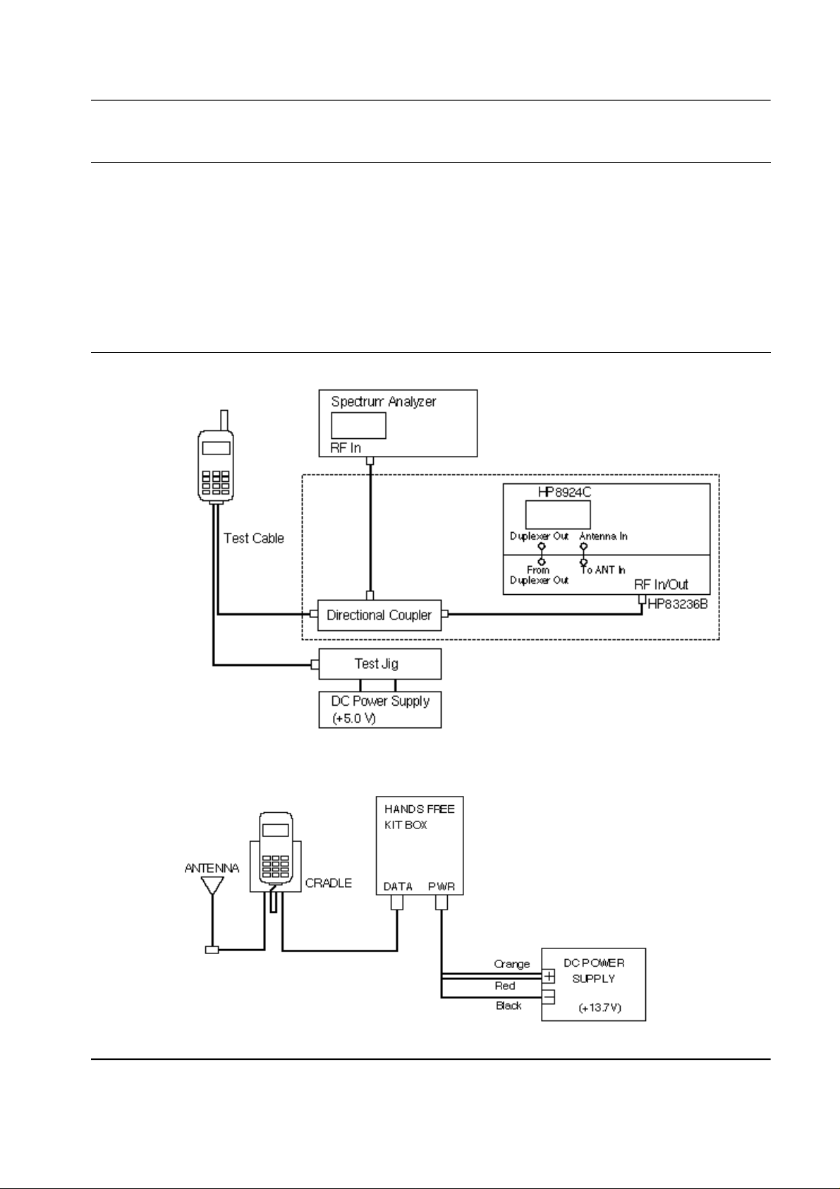
5. Test Procedure
5-1 List of Equipment
¶UDC Power Supply
¶UTest Jig
¶UTest Cable
¶UCDMA Mobile Station Test Set HP8924C, HP83236B, CMD-80, etc
¶USpectrum Analyzer (include CDMA test mode) HP8596E
5-2 Configuration of Test
5-2-1 Hand Set
5-2-2 Hand-Free
Samsung Electronics 5-1

Test Procedure
5-3 Test Procedure
5-3-1 Change to Test Mode
1. To change the phone from Normal Mode to test
Mode, You should enter the following keys.
" 4 7 * 8 6 9 # 1 2 3 5 "
2. The command ° ∞0 1"(Suspend) is entered to start
test.
3. To finish the Test Mode, You should enter the
command "0 2".
5-3-2 Channel Selection and Tx Power
Output level Control
1. You should change the phone from Normal
Mode to Test mode
2. The command ° ∞0 1"(Suspend) is entered to start
test.
3. You should enter the following keys.
" 0 9, 0 5 2 5, #, 0 7, 3 4, 7 1, 4 7 5, #"
¶UIf you enter the command "0 9", You can select
the channel
ex) 0 9 X X X X (means channel number)
¶UThe command "0 7°±means Carrier On (Carrier
Off : ° ∞0 8°±)
¶UIf you enter the command "3 4", You can
spread the carrier.
¶UIf you enter the command "7 1", You can
control the power output level. Following
under-bar means AGC code. And you can
control the power output level using Volume
Up/Down Keys.
ex) 7 1 X X X
4. After enter the command "7 4" and control the
Tx Power Output Level to be 0.0dBm using
Volume Up/Down keys, press "STO" key to
store Data in EEPROM.
5-2 Samsung Electronics

Test Procedure
5-4 Test Command Table
Command No. Test Command Description
(OP, AB, RB)
01(1F, 0, 0) T_SUSPEND_I Terminate the normal mode, enter to the test mode.
02(3F, 0, 0) T_RESTART_I Terminate the test mode, enter to the normal mode.
03(FD, 0, 0) T_SAVE_VAL_I Save value in EEPROM. (Only for Auto test)
04(1D, 0, 1) T_GET_MODE_I Get mode. (CDMA or FM)
05(1C, 1, 0) T_SET_MODE_I Set mode to CDMA or FM. (Only for Auto test)
06(1E, 0, 0) T_WRITE_NV_I Write an EEPROM item. (one of the NV items)
07(81, 0, 0) T_CARRIERON_I Turn the carrier on.
08(82, 0, 0) T_CARRIEROFF_I Turn the carrier off.
09(83, 4, 0) T_LOADSYN_I Set the synthesizer to the channel specified by ch_ data.
10(84, 1, 0) T_PWRLEVEL_I Set the RF power attenuation to the specified value.
11(85, 0, 0) T_RXMUTE_I Mute the receive-audio signal.
12(86, 0, 0) T_RXUNMUTE_I Unmute the receive-audio signal.
13(87, 0, 0) T_TXMUTE_I Mute the transmit-audio signal.
14(88, 0, 0) T_TXUNMUTE_I Unmute the transmit-audio signal.
16(8F, 0, 0) T_STON_I Turn on ST.
17(90, 0, 0) T_STOFF_I Turn off ST.
22(91,96,96) T_SNDNAM_I Display and send NAM information.
23(95, 3, 4) T_SNDVERSION_I Display and return S/W version.
24(9F, 7, 8) T_SNDESN_I Display and return ESN.
25(92, 0, 0) T_BACKLIGHT_ON_I Turn on the backlight.
26(93, 0, 0) T_BACKLIGHT_OFF_I Turn off the backlight.
27(96, 0, 0) T_LAMP_ON_I Turn on the LAMP.
28(97, 0, 0) T_LAMP_OFF_I Turn off the LAMP.
29(9A, 0, 0) T_REBUILD_I Rebuild EEPROM.
30(9D,15, 0) T_PLINE_I Display and return production date.
32(A0, 1, 0) T_SATON_I Turn on SAT.
33(A1, 0, 0) T_SATOFF_I Turn off SAT.
34(A2, 0, 0) T_CDATA_I Continuously send TX control data.
35(A3, 0, 0) T_VOLUME_UP_I Increase value of the last command. (Only for autotest)
36(A4, 0, 0) T_VOLUME_DOWN_I Decrease value of the last command. (Only for autotest)
42(AA, 1, 0) T_DTMFON_I Activate dtmf generator with keycode.
43(AB, 0, 0) T_DTMFOFF_I Deactivate DTMF generator.
44(B0, 0, 0) T_COMPANDORON_I Turn on compandor.
45(B1, 0, 0) T_COMPANDOROFF_I Turn off compandor.
50(B6, 4, 0) T_H_LIST_I History Channel.
57(BC, 0, 0) T_MIC_ON_I Mic path on.
58(BD, 0, 0) T_MIC_OFF_I Mic path off.
59(BE, 0, 0) T_ALLPATH_I Set RX Path, TX Path Unmute to Earpiece.
67(C6, 3, 6) T_READ_BATT_I Reads Low-Battery in the standby, talk.
Samsung Electronics 5-3

Test Procedure
Command No. Signal. Name Description
(OP, AB, RB)
68(C8, 0, 3) T_VBATT1_I Set the low battery position in the standby.
69(C9, 0, 3) T_VBATT2_I Set the low battery position in the talking.
70(CA, 3, 0) T_WRITE_BATT_I Write low battery level value to NVM.
71(D1, 3, 0) T_CDMA_TXADJ_I Change PDM TX AGC in CDMA.
72(D2, 3, 0) T_FM_TXADJ_I Change PDM TX AGC in FM.
73(D3, 1, 0) T_SET_PA_R_I Set PA R1, R0 in CDMA.
74(D4, 3, 0) T_TXADJ_0DBM_I Set TX AGC ADJ for 0dBm power.
75(D5, 0, 3) T_READ_RSSI_I Read a RSSI.
76(D6, 3, 0) T_WRITE_RSSI_I Writes RSSI.
77(D7, 0, 3) T_READ_TEMP_I Read Temp.
79(D9, 1, 0) T_BUZZER_ON_I Buzzer On at DTMF 0 key.
80(DA, 0, 0) T_BUZZER_OFF_I Buzzer off.
81(E3, 0, 0) T_VOC_PCMLPON_I Play a PCM LOOP BACK.
82(E4, 0, 0) T_VOC_PCMLPOFF_I Play off a PCM LOOP BACK.
84(E6, 3, 0) T_CD_MAX_LIMIT_I CDMA MAX limit.
85(E7, 0, 0) T_SPEAKER_ON_I Turn on the speaker path.
86(E8, 0, 0) T_SPEAKER_OFF_I Turn off the speaker path.
87(E9, 0, 0) T_FM_LOOP-TEST_I Play a PCM FM loopback.
88(EA, 3, 0) T_TRK_ADK_I TRK LOCAL ADJUST.
89(EB, 3, 0) T_CD_TRK_ADJ_I CDMA TRK LOCAL ADJUST.
90(F0, 3, 0) T_CDMA_LOW_CH_HIPWR_I Setting the volume for LOW CH highpwr. (+18dBm)
91(F1, 3, 0) T_CDMA_LOWMID_CH_HIPWR_I Setting the volume for LOWMID CH highpwr. (+18dBm)
92(F2, 3, 0) T_CDMA_MIDDLE_CH_HIPWR_I Setting the volume for MIDDLE CH highpwr. (+18dBm)
93(F3, 3, 0) T_CDMA_LOW_CH_LOPWR_I Setting the volume for LOW CH lowpwr. (-41dBm)
94(F4, 3, 0) T_CDMA_LOWMID_CH_LOPWR_I Setting the volume for LOWMID CH lowpwr. (-41dBm)
95(F5, 3, 0) T_CDMA_MIDDLE_CH_LOPWR_I Setting the volume for MIDDLE CH lowpwr. (-41dBm)
96(F6, 3, 0) T_CDMA_HIGHMID_CH_LOPWR_I Setting the volume for HIGHMID CH lowpwr. (-41dBm)
97(F7, 3, 0) T_CDMA_HIGH_CH_LOPWR_I Setting the volume for HIGH CH lowpwr. (-41dBm)
98(F8, 3, 0) T_CDMA_HIGHMID_CH_HIPWR_I Setting the volume for HIGHMID CH highpwr. (+18dBm)
99(F9, 3, 0) T_CDMA_HIGH_CH_HIPWR_I Setting the volume for HIGH CH highpwr. (+18dBm)
¶S
OP: Operation Command Number
AB: Input Argument Byte Number
RB: Return Byte Number
5-4
Samsung Electronics
 Loading...