

Samsung S6A0072 Datasheet

16COM/40SEG DOT MATRIX LCD CONTROLLER & DRIVER S6A0072
INTRODUCTION
S6A0072 is a dot matrix LCD driver & controller IC which is fabricated by low power CMOS technology. It is
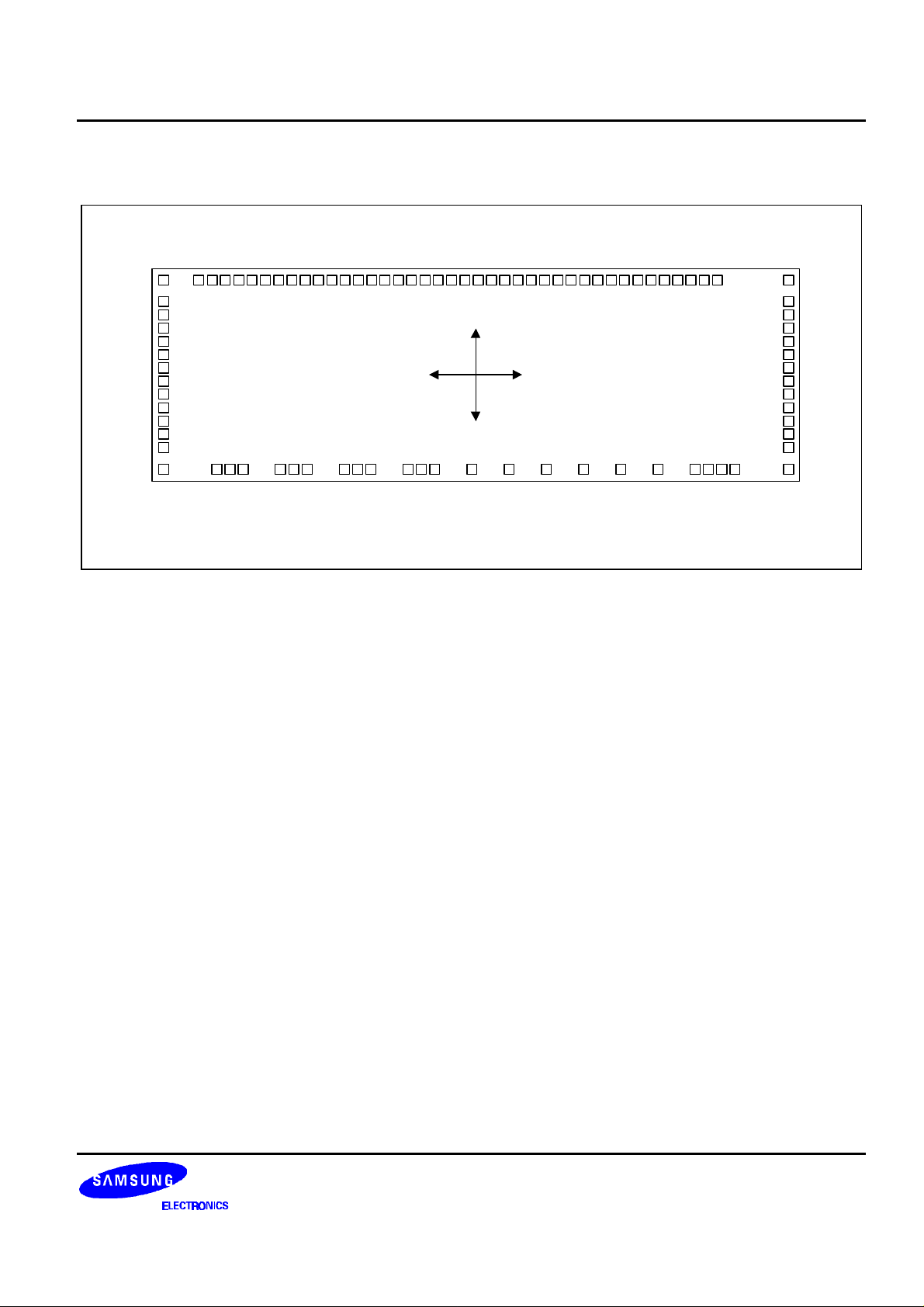
capable of displaying 1-line 16 characters or 2-line 8 characters with 5 × 8 dots format.
FUNCTIONS
Character type dot matrix LCD driver & controller
• Easy interface with 4-bit or 8-bit MPU.
• Internal driver: 16 common and 40 segment signal output.
• Display character pattern: 5 × 8 dots format (240 kinds)
• Direct programming of the special character patterns by character generator RAM
• Mask option for programming customer character patterns
• Various instruction functions
• Automatic power on reset
FEATURES
• Internal Memory
- Character Generator ROM (CGROM): 9600 bits (240 characters × 5 × 8 dot)
- Character Generator RAM (CGRAM): 160 bits (4 characters × 5 × 8 dot)
- Display Data RAM (DDRAM): 128 bits (16 characters × 8bits)
• Low power operation
- Power supply voltage range: 2.7 to 5.5V (VDD)
- LCD drive voltage range: 3.0 to 11.0 (VDD-V5)
• CMOS process
• Duty cycle: 1/16
• Built-in oscillator
• Low power consumption
• Internal divide resistor for LCD driving voltage
• COG available
1
S6A0072 16COM/40SEG DOT MATRIX LCD CONTROLLER & DRIVER
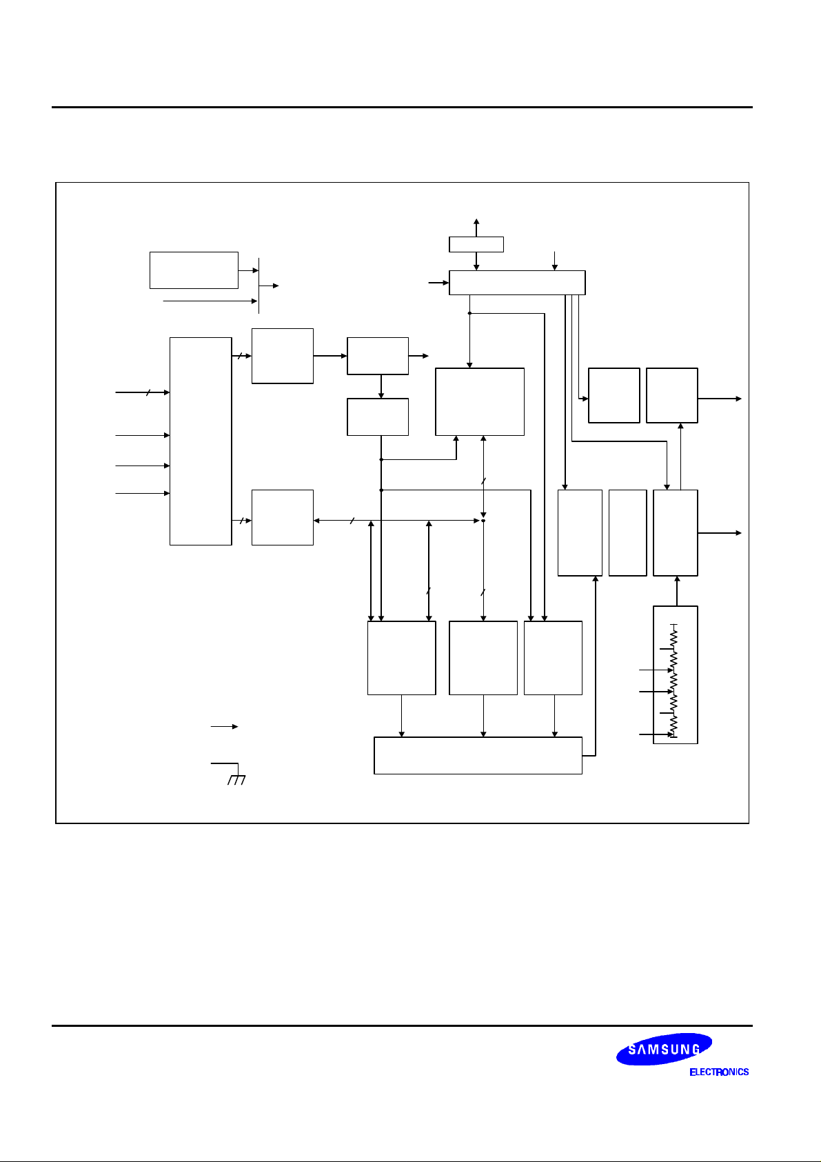
BLOCK DIAGRAM
TEST
DB0-DB7
R/W
RS
E
RESET
Power on Reset
(POR)
8
Input
Buffer
VDD
GND(VSS)
Instruction
8
Register
(IR)
Data
8 8
Register
(DR)
EXT_INT
Instruction
Decoder
Address
Counter
Character
Generator
(CGRAM)
32 bytes
Oscillator
Display Data
RAM (DDRAM)
16 x 8-bit
8
Character
Generator
RAM
(CGROM)
9600 bits
Parallel to Serial Converter
Timing Generator
8
8
ROM
EXTCLK
Register
Cursor
Blink
Control
Circuit
40-bit
Shift
16-bit
Shift
Register
40-bit
Latch
Circuit
V2
V3
V5
Common
Driver
Segment
Driver
VDD
V1
V4
C1-C16
S1-S40
2
16COM/40SEG DOT MATRIX LCD CONTROLLER & DRIVER S6A0072
PAD DIAGRAM
C16
C15
C14
C13
C12
C11
C10
C9
TEST
DUMMY
DUMMY
DUMMY
S6A0072
DUMMY DUMMY
S40
S37
S38
S39
DUMMY
EXTCLK
EXT_INT
S36
S35
S34
VSS
S33
VSS
S32
VSS
S31
S30
S28
S29
VDD
VDD
S26
S27
VDD
S24
S25
V5V5V5
S23
S22
(0, 0)
S21
S20
Y
V3
S19
S18
S17
V2
S16
X
S14
S15
RESET
S13
S12
S11
RS
S10
S9
S8
R/W
S7
S6
DUMMY
S1
S2
S3
S4
S5
S6A0072
C8
C7
C6
C5
C4
C3
C2
C1
DB7
DB6
DB5
DB4
E
DB1
DB0
DB2
DB3
DUMMY
Chip Size: 7600 × 2160 µm
Pad pitch: min. 125 µm
Chip thickness 675 µm
Al Pad Specifications
AL pad size on Y side: 87 × 94 µm
AL pad size on X side: 94 × 87 µm
Au Bump Specifications
Bump size on Y side: 77 × 84 µm
Bump size on X side: 84 × 77µm
Bump height: 18 ± 1µm
3
S6A0072 16COM/40SEG DOT MATRIX LCD CONTROLLER & DRIVER
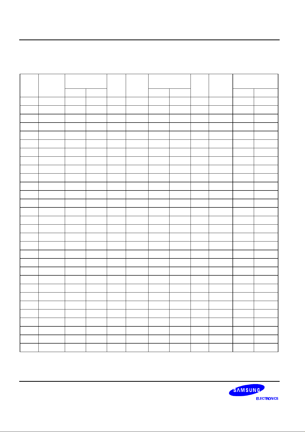
PAD CENTER COORDINATES
Unit: um
Pad
No.
X Y X Y X Y
1 DUMMY -3642 -881 31 C3 3643 64 61 S24 -455 923
2 DUMMY -3032 -881 32 C4 3643 189 62 S25 -580 923
3 EXTCLK -2632 -881 33 C5 3643 314 63 S26 -705 923
4 EXT_INT -2232 -881 34 C6 3643 439 64 S27 -830 923
5 VSS -1832 -881 35 C7 3643 564 65 S28 -955 923
6 VSS -1707 -881 36 C8 3643 689 66 S29 -1080
7 VSS -1582 -881 37 DUMMY 3643 923 67 S30 -1205
8 VDD -1182 -881 38 S1 2464 923 68 S31 -1330
9 VDD -1057 -881 39 S2 2329 923 69 S32 -1455
10 VDD -932 -881 40 S3 2204 923 70 S33 -1580
11 V5 -532 -881 41 S4 2079 923 71 S34 -1705
12 V5 -407 -881 42 S5 1954 923 72 S35 -1830
13 V5 -282 -881 43 S6 1829 923 73 S36 -1955
14 V3 117 -881 44 S7 1704 923 74 S37 -2080
15 V2 517 -881 45 S8 1579 923 75 S38 -2205
16 RESETB 917 -881 46 S9 1454 923 76 S39 -2330
17 RS 1317 -881 47 S10 1329 923 77 S40 -2463
18 R/W 1717 -881 48 S11 1204 923 78 DUMMY -3642
19 E 2117 -881 49 S12 1079 923 79 C16 -3643
20 DB0 2521 -881 50 S13 954 923 80 C15 -3643
21 DB1 2697 -881 51 S14 829 923 81 C14 -3643
22 DB2 2871 -881 52 S15 704 923 82 C13 -3643
23 DB3 3047 -881 53 S16 579 923 83 C12 -3643
24 DUMMY 3643 -881 54 S17 454 923 84 C11 -3643
25 DB4 3643 -717 55 S18 329 923 85 C10 -3643
26 DB5 3643 -591 56 S19 204 923 86 C9 -3643
27 DB6 3643 -467 57 S20 71 923 87 TEST -3643
28 DB7 3643 -341 58 S21 -70 923 88 DUMMY -3643
29 C1 3643 -184 59 S22 -205 923 89 DUMMY -3643
30 C2 3643 -60 60 S23 -330 923 90 DUMMY -3643
Pad
Name
Coordinate Pad
No.
Pad
Name
Coordinate Pad
No.
Pad
Name
Coordinate
923
923
923
923
923
923
923
923
923
923
923
923
923
689
564
439
314
189
64
-60
-184
-341
-467
-592
-717
4
16COM/40SEG DOT MATRIX LCD CONTROLLER & DRIVER S6A0072
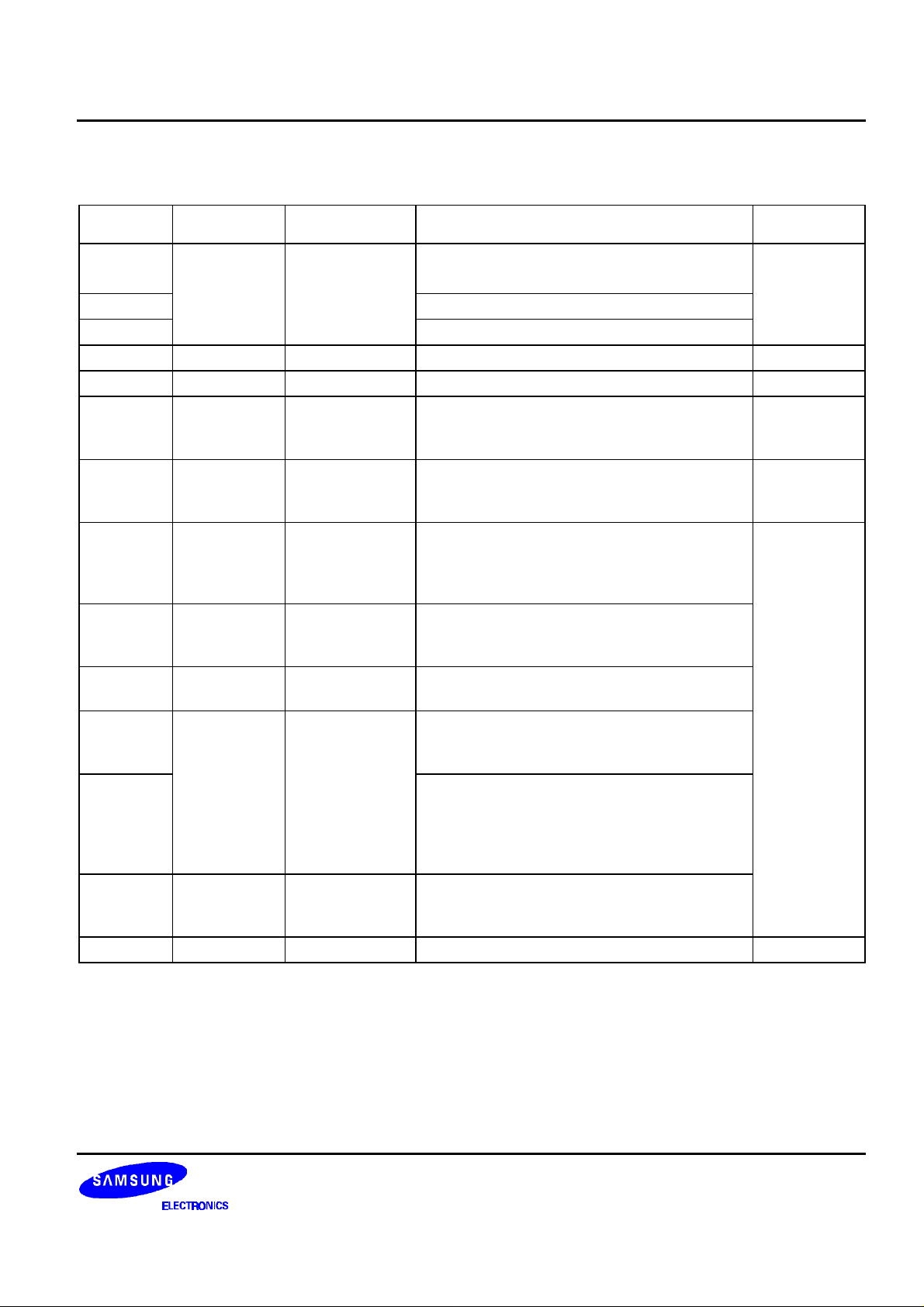
PIN DESCRIPTION
Pin
VDD Power Power supply &
VSS (GND)
V2, V3, V5
S1 - S40 Output Segment output Segment signal output for LCD driving LCD
C1 - C16 Input Common output Common signal output for LCD driving LCD
EXTCLK Input External clock
EXT_INT Input External/internal
RS Input Register select Used as register selection input.
R/W Input
E Input Read/write
DB0-DB3 Input/Output Data bus 0 - 7 When 8-bit bus mode, used as low order
DB4-DB7
RESETB Input Reset If it is necessary to initialize the system by
TEST Output Test pin Internal oscillator test pin. Open this pin. Open
Input/Output
0V (GND)
Bias voltage level for LCD driving
When 8-bit bus mode, used as high order bi-
Name Description Interface
for logical circuit (+3V, +5V) Power supply
LCD bias pin
When using external clock, used as clock
Input
oscillator clock
select
Read/write Used as read/write selection input.
enable
input pin. When using internal oscillator,
connect to VDD or VSS.
When EXT_INT = "High", external clock is
used. When "Low", internal oscillator is used.
When RS = "High", Data register is selected.
When RS = "Low", Instruction register is
selected.
When R/W = "High", read operation.
When R/W = "Low", write operation.
Used as read/write enable signal.
bi-directional data bus.
During 4-bit bus mode open these pins.
directional data bus. In case of 4-bit bus
mode, used as both high and low order.
DB7 is used for busy flag output during read
instruction operation.
hardware, force "Low", level signal to this
terminal about 1.2ms.
External clock
VDD/VSS
MPU
5
S6A0072 16COM/40SEG DOT MATRIX LCD CONTROLLER & DRIVER
FUNCTION DESCRIPTION
SYSTEM INTERFACE
This chip consists of two kinds of interface type with MPU: 4-bit bus and 8-bit bus. 4-bit bus and 8-bit bus is
selected by DL bit of function set in the instruction register. During read or write operation, two 8-bit registers are
used. One is the data register (DR), the other is the instruction register (IR). The data register (DR) is used as a
temporary data storage place for being written into or read from DDRAM/CGRAM, target RAM is selected by
RAM address setting instruction. Each internal operation, reading from or writing into RAM, is done automatically.
Thus, after MPU reads DR data, the data in the next DDRAM/CGRAM address is transferred into DR
automatically. Also after MPU writes data to DR, the data in DR is transferred into DDRAM/CGRAM
automatically. The Instruction register (IR) is used only to store instruction code transferred from MPU. MPU
cannot read data from instruction register. The register selection depends on RS input pin setting in both 4-bit bus
mode.
Table 1. Various Kinds Of Operations According to RS and R/W Bits
RS R/W Operation
0 0 Instruction write operation (MPU writes Instruction code into IR)
0 1 Read busy flag (DB7) and address counter (DB0 - DB6)
1 0 Data write operation (MPU writes data into DR)
1 1 Data read operation (MPU reads data from DR)
BUSY FLAG (BF)
BF = "High" indicates that the internal operation is being processed. So during this time the next instruction
cannot be accepted. BF can be read, when RS = Low and R/W = High (Read instruction Operation), through DB7
port.
Before executing the next instruction, be sure that BF is not High.
ADDRESS COUNTER (AC)
Address Counter (AC) stores the address of DDRAM/CGRAM that are transferred from IR. After writing into
(reading from) DDRAM/CGRAM data, AC is increased (decreased) by 1 automatically. When RS = "Low", and
R/W = "High", AC value can be read through DB0 - DB6 ports.
6
16COM/40SEG DOT MATRIX LCD CONTROLLER & DRIVER S6A0072
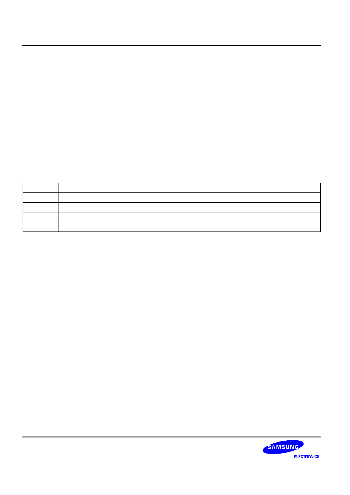
DISPLAY DATA RAM (DDRAM)
DDRAM stores 8bits character code in CGROM/CGRAM and its maximum number is 16 (16 Characters).
DDRAM address is set by the address counter (AC) as hexadecimal number.
MSB LSB
AC6 AC5 AC4 AC3 AC2 AC1 AC0
HEXHEX
The relations of DDRAM address and display position is as follows.
1) DDRAM Addressing Mode 0 (A = 0)-
In this addressing mode, the address range of DDRAM is 00H - 0FH.
After Shift Left:
After Shift Right:
1 2 3 4 5
00 01 02 03 04
COM1 - COM8 COM9 - COM16
COM1
COM8
COM1
COM8
1 2 3 4 5
01 02 03 04
1 2 3 4 5
0F 00
6 7 8 9 10 11 12 13 14 15
05 06 07 08 09 0A 0E 0F
6 7 8 9 10 11 12 13 14 15
05 06 07 08 09 0A 0E 0F1600
6 7 8 9 10 11 12 13 14 15
01 02 03 04
05 06 07 08 09 0A 0E
0B 0C 0D
0B 0C 0D
16
0B 0C 0D
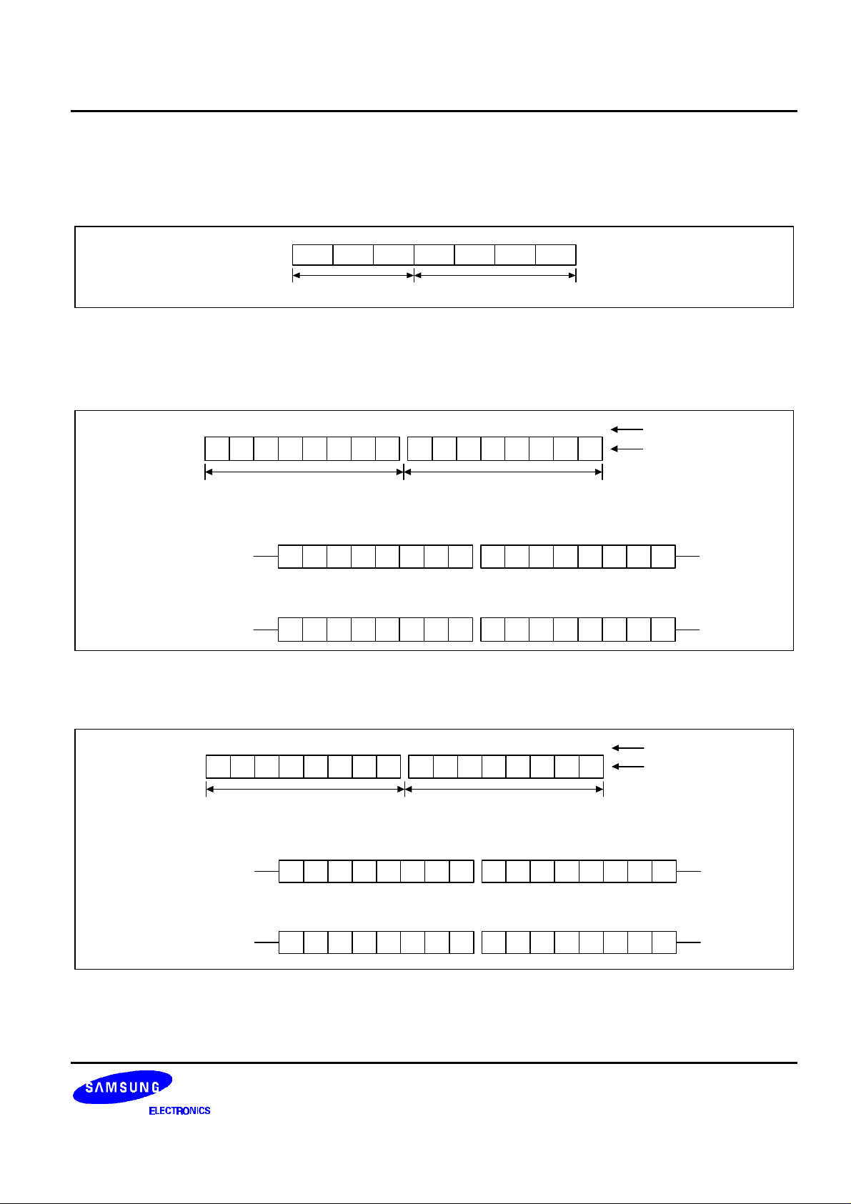
2) DDRAM Addressing Mode 1 (A = 1)
In this addressing mode, the address range of DDRAM is 00H - 07H and 40H - 47H.
1 2 3 4 5
00 01 02 03 04
COM1 - COM8 COM9 - COM16
6 7 8 9 10 11 12 13 14 15
05 06 07 40 41 42 46 47
43 44 45
16
Display Position
DDRAM Address
COM9
COM16
16
COM9
COM16
Display Position
DDRAM Address
After Shift Left:
After Shift Right:
COM1
COM8
COM1
COM8
1 2 3 4 5
01 02 03 04
1 2 3 4 5
4F 00
01 02 03 04
6 7 8 9 10 11 12 13 14 15
05 06 07 40
6 7 8 9 10 11 12 13 14 15
05 06
43 44 4541 42 46 47 00
16
COM9
COM16
16
43 44 4541 42 464007
COM9
COM16
7
S6A0072 16COM/40SEG DOT MATRIX LCD CONTROLLER & DRIVER
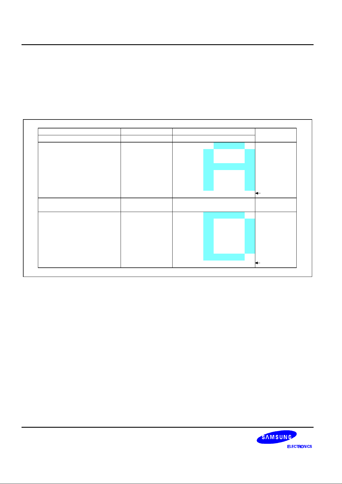
CHARACTER GENERATOR RAM (CGRAM)
CGRAM is used for user defined character pattern. The format of the character pattern is 5 × 7 dots except for
the cursor position and has a maximum of 4 characters. To use the character pattern in CGRAM write the
character code into DDRAM as shown in table 2.
Table 2. Relationship Between Character Code (DDRAM) and Character Pattern (CGRAM)
Character Code (DDRAM data) CGRAM Address CGRAM Data
D7 D6 D5 D4 D3 D2 D1 D0 A4 A3 A2 A1 A0 P7 P6 P5 P4 P3 P2 P1 P0
0 0 *0 * 0 0 0 0 0 0 0
0 0 0 *0 * 1 1 1 1 0 0 0
NOTE: "∗" don’t care.
Pattern
Number
x x x 0 0
0 0
.
.
.
.
.
.
.
.
.
.
.
.
0 0
0 0
0 0
0 0
0 0
0 0
.
.
1 1
1 1
1 1
1 1
1 1
1 1
1 1
0 0
0 0
0
1
1 1
1 1
1 1 1
0 0
0 0
0
1
1 1
1 1
1 1 1
1
1 1
0 0
0
.
.
1
1 1
0 0
0
1
0
1
0
.
.
.
.
.
x x x
.
.
.
.
.
1 1 10
1
0 0 0
1
0 0 0
1
1 1 1 1
1
0 0 0
1
0 0 0
1
0 0 0
0
0 0 0 0
.
.
11 01 1
1
0 0 0
1
0 0 0
1
0 0 0 1
1
0 0 0
1
0 0 0
1
1 1 1
0
0 0 0 0
Pattern 1
1
1
1
1
1
Cursor position
.
.
Pattern 4
1
1
1
1
0
Cursor position
8

16COM/40SEG DOT MATRIX LCD CONTROLLER & DRIVER S6A0072
CHARACTER GENERATOR ROM (CGROM)
CGROM generates 5 × 8 character pattern from character generate code in DDRAM. CGROM has 5 × 8-dot 240
character pattern including cursor position. If the data in cursor position bit are high, the data are included to the
character pattern. So, the selected positions are always "ON" regardless to cursor position. The relationship
between character code and character pattern can be referred to table 5.
TIMING GENERATION CIRCUIT
Timing generation circuit generates clock signals for the internal operations.
LCD DRIVER CIRCUIT
LCD driver circuit has 16 common and 40 segment output signals for LCD driving. Data from CGRAM/CGROM is
transferred to 40-bit segment shift register serially, then it is stored to 40-bit segment output latch. When each
com is selected by a 16-bit common register, the segment data also outputs through segment driver from 40-bit
segment output latch.
CURSOR/BLINK CONTROL CIRCUIT
It controls cursor/blink ON/OFF at the cursor position.
9

S6A0072 16COM/40SEG DOT MATRIX LCD CONTROLLER & DRIVER
INSTRUCTION DESCRIPTION
OUTLINE
To overcome the speed difference between the internal clock of S6A0072 and the MPU clock, the S6A0072
performs an internal operation by storing control information to IR or DR. The internal operation is determined
according to the signal from MPU, composed of read/write and data bus.
Instruction can be divided into four types:
• S6A0072 function set instructions (set display methods, set data length, etc.)
• Address set instructions to internal RAM
• Data transfer instructions with internal RAM
• Others.
The address of internal RAM is automatically increased or decreased by 1.
NOTE: During an internal operation, the busy flag (DB7) is high. Busy flag check must precede the next instruction.
When an MPU program with busy flag (DB7) checking is made, 1/2Fosc is necessary for executing the next
instruction by the falling edge of the "E" signal after the busy flag (DB7) goes to "Low".
10
 Loading...