

40 SEG / 16 COM DRIVER & CONTROLLER FOR DOT MATRIX LCD
S6A0069
written permission of LCD Driver IC Team.
June. 2000.
Ver. 0.0
Contents in this document are subject to change without notice. No part of this document may be reproduced
or transmitted in any form or by any means, electronic or mechanical, for any purpose, without the express

S6A0069 40 SEG / 16 COM DRIVER & CONTROLLER FOR DOT MATRIX LCD
INTRODUCTION
S6A0069 is a dot matrix LCD driver & controller LSI which is fabricated by low power CMOS technology. It can
display 1, 2-line with 5 x 8 or 5 x 11 dots format.
FUNCTIONS
• Character type dot matrix LCD driver & controller.
• Internal driver: 16 common and 40 segment signal output.
• Easy interface with 4-bit or 8-bit MPU
• Display character pattern : 5 x 8 dots format (204 kinds), 5 x 11 dots format (32 kinds)
• The special character pattern can be programmable by Character Generator RAM directly.
• A customer character pattern can be programmable by mask option.
• It can drive a maximum 80 characters by using the S6A0065 or S6A2067 externally.
• Various instruction functions
• Automatic power on reset
FEATURES
• Internal Memory
- Character Generator ROM (CGROM): 10,080 bits (204 characters x 5 x 8 dot) & ( 32 characters x 5 x 11
dot)
- Character Generator RAM (CGRAM): 64 × 8 bits (8 characters × 5 × 8 dot)
- Display Data RAM (DDRAM): 80 x 8 bits (80 characters max.)
• Low Power Operation
- Power supply voltage range: 2.7 to 5.5V (VDD)
- LCD drive voltage range: 3.0 to 13.0V (VDD - V5)
• CMOS process
• Programmable duty cycle: 1/8, 1/11, 1/16
• Internal oscillator with an external resistor
• Low power consumption
• Bare chip available
2
40 SEG / 16 COM DRIVER & CONTROLLER FOR DOT MATRIX LCD S6A0069
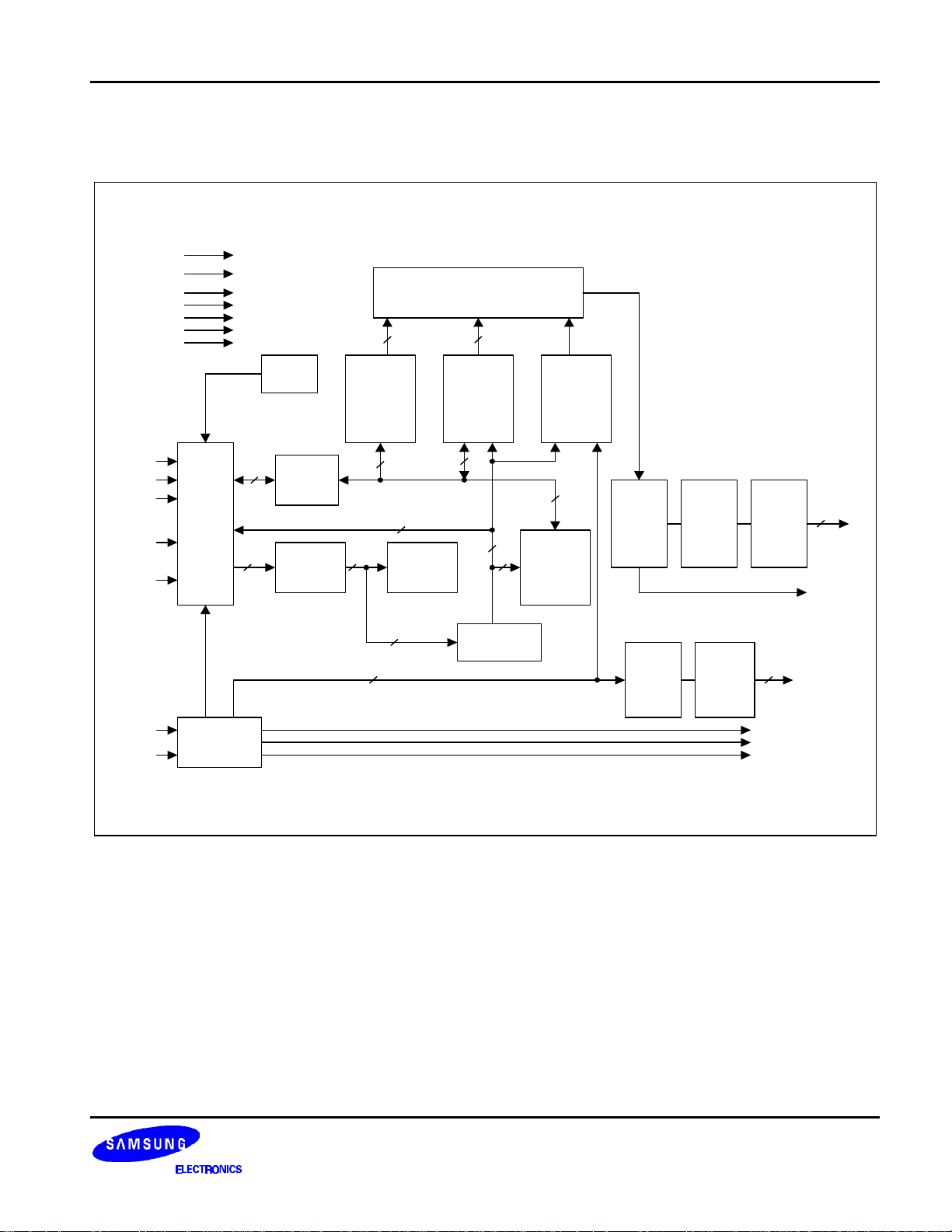
BLOCK DIAGRAM
VDD
GND
V1
V2
V3
V4
V5
Busy
Flag
Character
Generator
ROM
(CGROM)
10080 bits
Parallel to Serial
Data Conversion Circuit
55
Character
Generator
RAM
(CGRAM)
512 bits
Cursor
& Blink
Controller
R/W
RS
DB0-
DB3
DB4-
DB7
OSC1
OSC2
8
7
7
Address
Counter
8
Display
Data RAM
(DDRAM)
80x8 bits
40-bit
Shift
Register
16-bit
Shift
Register
40-bit
Latch
Circuit
Common
Driver
Segment
Driver
16
C1-C16
CLK1
CLK2
M
40
S1-S40
D
8
8
8
Instruction
Decoder
(ID)
7
7
Data
8
Register
8
(DR)
Instruction
Register
(IR)
E
Input/
Output
Buffer
Timing
Generator
Circuit
3
S6A0069 40 SEG / 16 COM DRIVER & CONTROLLER FOR DOT MATRIX LCD
OSC2
CLK1
CLK2
VDD
R/W
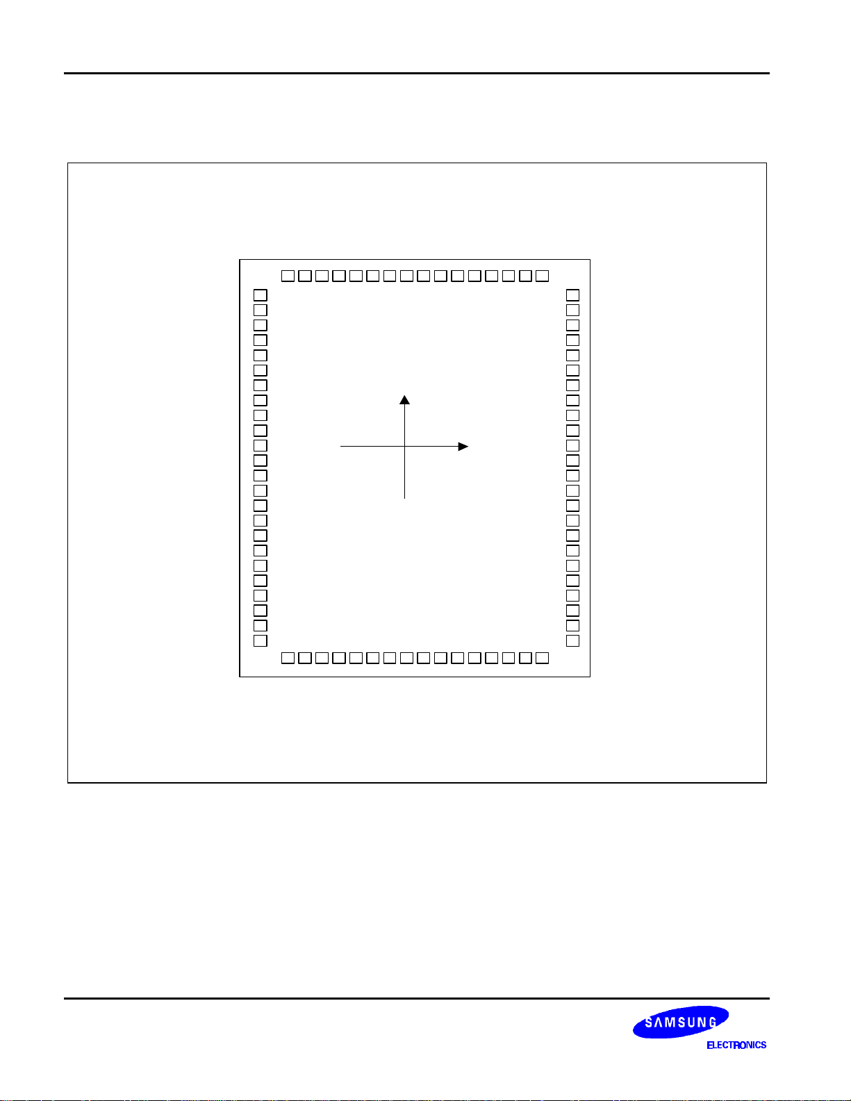
PAD CONFIGURATION
S23
S24
S25
S26
S27
S28
S29
S30
S31
S32
S33
S34
S35
S36
S37
S38
807978777675747372717069686766
65
S22
S21
S20
S19
S18
S17
S16
S15
S14
S13
S12
S11
S10
S9
S8
S7
S6
S5
S4
S3
S2
S1
GND
OSC1
10
11
12
13
14
15
16
17
18
19
20
21
22
23
24
1
2
3
4
5
6
7
8
9
Chip size: 4060
Pad size: 100
Unit: µm
252627282930313233343536373839
V1V2V3V4V5
Y
(0, 0)
×
×
100
3840
M
X
D
S6A0069
RS
40
E
DB0
DB1
64
63
62
61
60
59
58
57
56
55
54
53
52
51
50
49
48
47
46
45
44
43
42
41
S39
S40
C16
C15
C14
C13
C12
C11
C10
C9
C8
C7
C6
C5
C4
C3
C2
C1
DB7
DB6
DB5
DB4
DB3
DB2
4
40 SEG / 16 COM DRIVER & CONTROLLER FOR DOT MATRIX LCD S6A0069
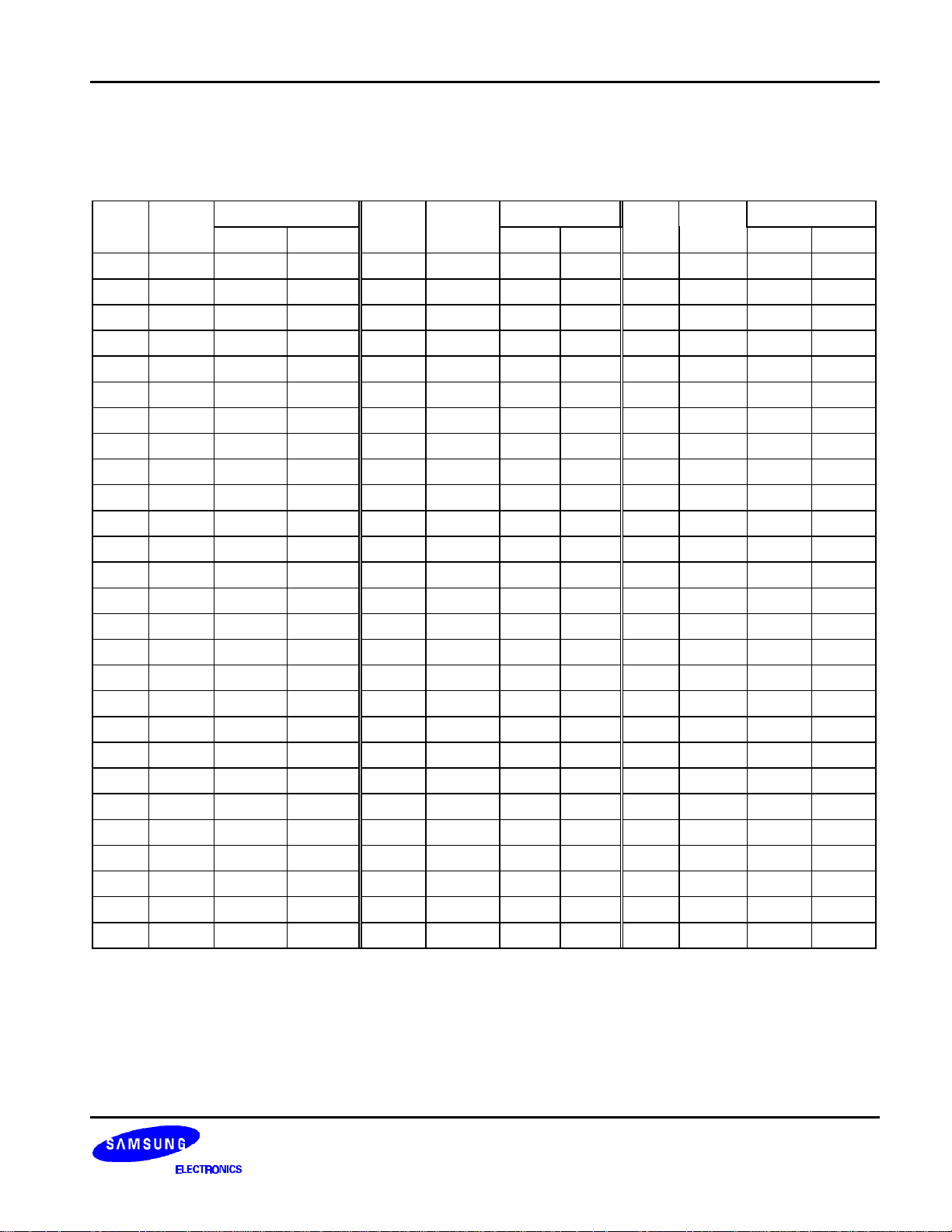
PAD CENTER COORDINATES
Unit: um
COORDINATE COORDINATE PAD PAD COORDINATEPAD
X Y
PAD
NUM.
PAD
NAME
X Y NUM. NAME X Y
NUM.
PAD
NAME
1 S22 -1864 1465 28 V3 -670 -1754 55 C9 1864 335
2 S21 -1864 1340 29 V4 -520 -1754 56 C10 1864 460
3 S20 -1864 1215 30 V5 -370 -1754 57 C11 1864 585
4 S19 -1864 1090 31 CLK1 -220 -1754 58 C12 1864 710
5 S18 -1864 965 32 CLK2 -70 -1754 59 C13 1864 835
6 S17 -1864 840 33 VDD 80 -1754 60 C14 1864 960
7 S16 -1864 715 34 M 230 -1754 61 C15 1864 1085
8 S15 -1864 590 35 D 380 -1754 62 C16 1864 1210
9 S14 -1864 465 36 RS 518 -1754 63 S40 1864 1341
10 S13 -1864 340 37 R/W 642 -1754 64 S39 1864 1466
11 S12 -1864 215 38 E 768 -1754 65 S38 886 1754
12 S11 -1864 90 39 DB0 894 -1754 66 S37 760 1754
13 S10 -1864 -35 40 DB1 1018 -1754 67 S36 636 1754
14 S9 -1864 -160 41 DB2 1864 -1488 68 S35 510 1754
15 S8 -1864 -285 42 DB3 1864 -1362 69 S34 386 1754
16 S7 -1864 -410 43 DB4 1864 -1238 70 S33 260 1754
17 S6 -1864 -535 44 DB5 1864 -1112 71 S32 136 1754
18 S5 -1864 -660 45 DB6 1864 -988 72 S31 10 1754
19 S4 -1864 -785 46 DB7 1864 -862 73 S30 -114 1754
20 S3 -1864 -910 47 C1 1864 -665 74 S29 -240 1754
21 S2 -1864 -1034 48 C2 1864 -540 75 S28 -364 1754
22 S1 -1864 -1159 49 C3 1864 -415 76 S27 -490 1754
23 GND -1864 -1285 50 C4 1864 -290 77 S26 -614 1754
24 OSC1 -1864 -1414 51 C5 1864 -165 78 S25 -740 1754
25 OSC2 -1120 -1754 52 C6 1864 -40 79 S24 -864 1754
26 V1 -970 -1754 53 C7 1864 85 80 S23 -989 1754
27 V2 -820 -1754 54 C8 1864 210
5
S6A0069 40 SEG / 16 COM DRIVER & CONTROLLER FOR DOT MATRIX LCD
PIN DESCRIPTION
PIN No I/O NAME DESCRIPTION INTERFACE
VDD
GND 0V (GND)
V1 - V5
S1 - S40
33
23
26- 30
1-22,
63- 80
Voltage
O Segment output Segment signal output for LCD drive. LCD
Supply
Supply Voltage for logical circuit (+3V ±
10%,+5V ±10%)
Power Supply
Bias voltage level for LCD driving.
C1 - C16 47-62 O Common output Common signal output for LCD drive. LCD
OSC1 24 I Oscillator
OSC2 25 O Oscillator
CLK1 31 O
CLK2 32 O
Extension driver
Latch clock
Extension driver
Shift clock
Alternated signal
M 34 O
for LCD driver
output
D 35 O
Display data
interface
When use internal oscillator, connect
external Rf resistor. If external clock is
used, connect it to OSC1.
extension driver latch clock.
extension driver shift clock.
Outputs the alternating signal to convert
LCD driver waveform to AC.
Outputs extension driver data (the 41th
dot's data)
External
Resistor/
Oscillator
OSC1
Extension
driver
Extension
driver
Extension
driver
Used as register selection input. When
RS 36 I Register select
RS = "High", Data register is selected.
When RS = "Low", Instruction register is
MPU
selected.
Used as read/write selection input.
R/W 37 I Read/Write
When R/W = "High", read operation.
MPU
When R/W = "Low", write operation.
E 38 I Read/write enable Read/write enable signal. MPU
DB0-
DB3
39-42
When 8-bit bus mode, used as low order
bidirectional data bus.
MPU
In 4-bit bus mode open these pins.
6
DB4-
DB7
43-46
I/O Data bus 0-7
When 8-bit bus mode, used as high
order bidirectional data bus. In case of 4bit bus mode, used as both high and low
order.
DB7 is used for Busy Flag output.
MPU
40 SEG / 16 COM DRIVER & CONTROLLER FOR DOT MATRIX LCD S6A0069
FUNCTION DESCRIPTION
System Interface
This chip has all two kinds of interface type with MPU : 4-bit bus and 8-bit bus. 4-bit bus and 8-bit bus is selected
by DL bit in the instruction register. During read or write operation, two 8-bit registers are used. one is data
register (DR), the other is instruction register(IR). The data register(DR) is used as temporary data storage place
for being written into or read from DDRAM/CGRAM. The target RAM is selected by RAM address setting
instruction. Each internal operation, reading from or writing into RAM, is done automatically. So to speak, after
MPU reads DR data, the data in the next DDRAM/CGRAM address is transferred into DR automatically. Also
after MPU writes data to DR, the data in DR is transferred into DDRAM/CGRAM automatically. The instruction
register (IR) is used only to store instruction code transferred from MPU. MPU cannot use it to read instruction
data. To select register, use RS input pin in 4-bit/8-bit bus mode.
Table 1. Various Kinds of Operations according to RS and R/W Bits
RS R/W Operation
L L Instruction Write operation (MPU writes Instruction code into IR)
L H Read Busy Flag (DB7) and address counter (DB0 - DB6)
H L Data Write operation (MPU writes data into DR)
H H Data Read operation (MPU reads data from DR)
Busy Flag (BF)
When BF = "High", it indicates that the internal operation is being processed. So during this time the next
instruction cannot be accepted. BF can be read, when RS = Low and R/W = High (Read Instruction Operation),
through DB7 port. Before executing the next instruction, be sure that BF is not High.
Address Counter (AC)
Address Counter(AC) stores DDRAM/CGRAM address, transferred from IR. After writing into (reading from)
DDRAM/CGRAM, AC is automatically increased (decreased) by 1. When RS = "Low" and R/W = "High", AC can
be read through DB0 - DB6 ports.
7
S6A0069 40 SEG / 16 COM DRIVER & CONTROLLER FOR DOT MATRIX LCD
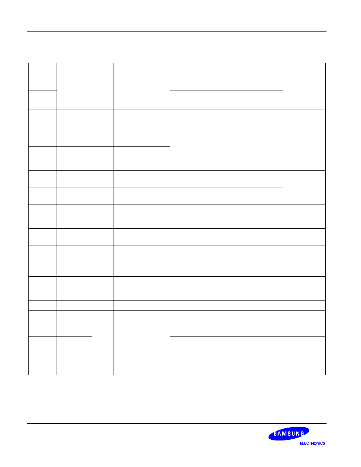
Display Data RAM (DDRAM)
DDRAM stores display data of maximum 80 x 8 bits (80 characters). DDRAM address is set in the address
counter (AC) as a hexadecimal number. (refer to Figure1.)
LSBMSB
AC6 AC5 AC4 AC3 AC2 AC1 AC0
Figure 1. DDRAM Address
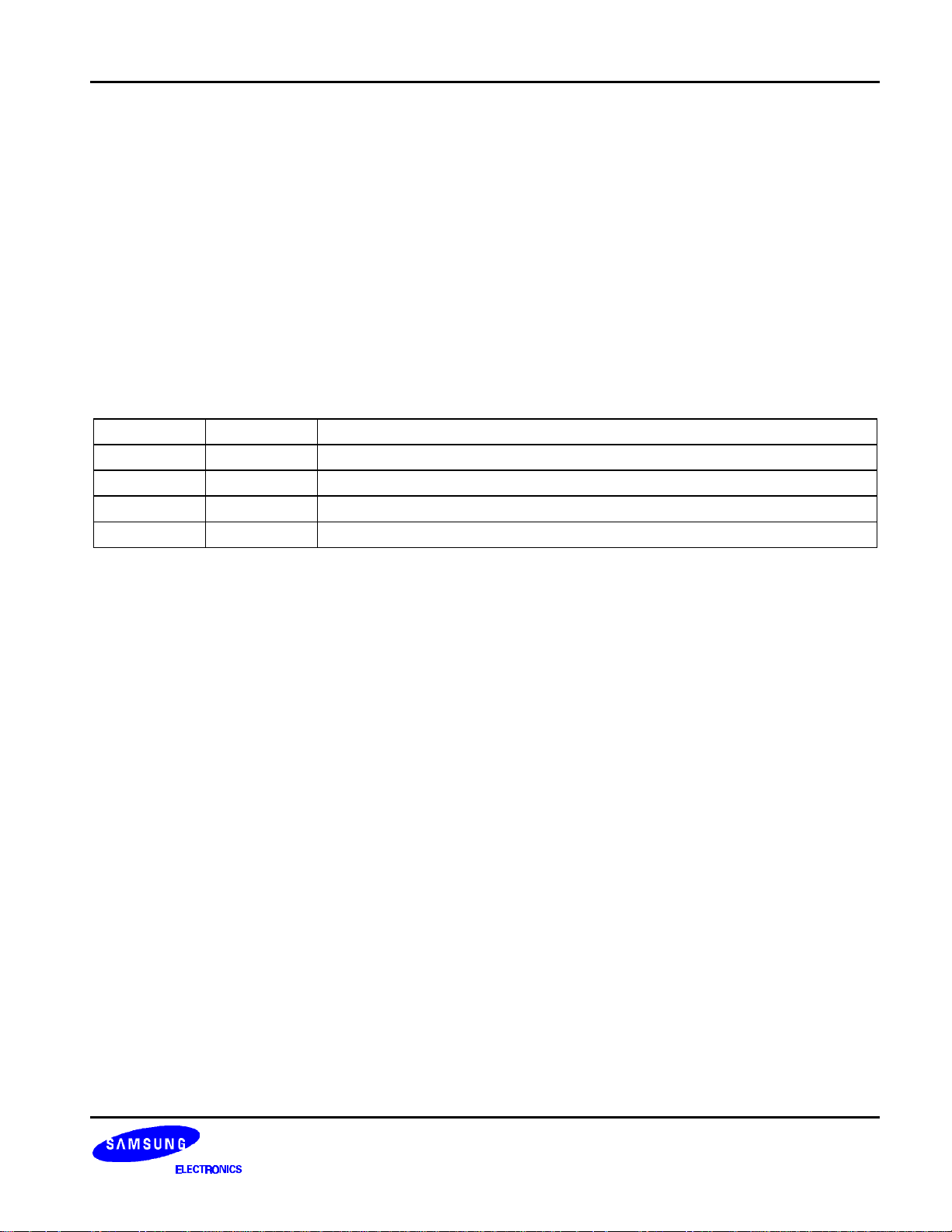
1) 1-line Display
In case of 1 line display, the address range of DDRAM is 00H - 4FH. Extension driver will be used. Fig-2 shows
the example that 40 segment extension driver is added.
1
2 3 4 5 6 7 8
COM1
COM8
COM1
COM8
COM1
COM8
00
01 02 03 04 05 06 07
SEG1 S6A0069 SEG40
1
2 3 4 5 6 7 8
01 02 03 04 05 06 07
SEG1 S6A0069 SEG40
1
2 3 4 5 6 7 8
00
4F
SEG1 S6A0069 SEG40
01 02 03 04 05 06 07
Figure 2. 1-line x 24 Character Display with 40 Segment Extension Driver
Display position
10 11 12 13 14 15 16
08909 0A 0B 0C 0D 0E 0F
SEG1 Extension driver (40 SEG) SEG40 SEG1 Extension driver (40 SEG) SEG40
9
10 11 12 13 14 15 16
08
09 0A 0B 0C 0D 0E 0F
SEG1 Extension driver (40 SEG) SEG40 SEG1 Extension driver (40 SEG) SEG40
(After Shift Left)
10 11 12 13 14 15 16
08909 0A 0B 0C 0D 0E 0F
SEG1 Extension driver (40 SEG) SEG40 SEG1 Extension driver (40 SEG) SEG40
(After Shift Right)
10
18 19 20 21 22 23 24
101711 12 13 14 15 16 17
DDRAM Address
17
18 19 20 21 22 23 24
11 12 13 14 15 16 17
18 19 20 21 22 23 24
101711 12 13 14 15 16
18
8
40 SEG / 16 COM DRIVER & CONTROLLER FOR DOT MATRIX LCD S6A0069
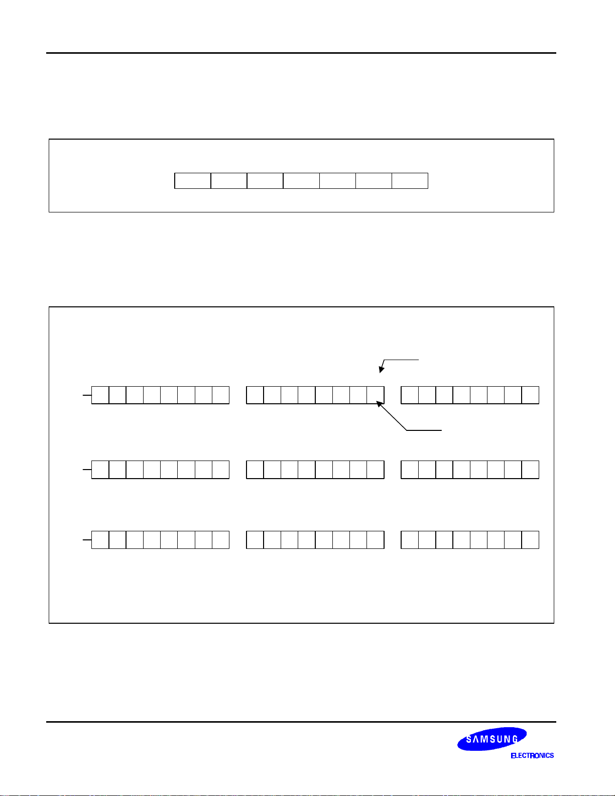
2) 2-line Display
In case of 2 line display, the address range of DDRAM is 00H - 27H, 40H - 67H. Extension driver will be used.
Figure 3 shows the example that 40 segment extension driver is added.
Display position
2 3 4 5 6 7 8
10 11 12 13 14 15 16
18 19 20 21 22 23 24
00101 02 03 04 05 06 07
40 41 42 43 44 45 46 47 48 49 4A 4B 4C 4D 4E 4F 50 51 52 53 54 55 56 57
SEG1 S6A0069 SEG40 SEG1 Extension driver (40 SEG) SEG40 SEG1 Extension driver (40 SEG) SEG40
1
2 3 4 5 6 7 8
01 02 03 04 05 06 07
41 42 43 44 45 46 47 48 49 4A 4B 4C 4D 4E 4F 50 51 52 53 54 55 56 57
SEG1 S6A0069 SEG40 SEG1 Extension driver (40 SEG) SEG40 SEG1 Extension driver (40 SEG) SEG40
2 3 4 5 6 7 8
00101 02 03 04 05 06 07
27
40 41 42 43 44 45 46 47 48 49 4A 4B 4C 4D 4E 4F 50 51 52 53 54 55 56
67
SEG1 S6A0069 SEG40 SEG1 Extension driver (40 SEG) SEG40 SEG1 Extension driver (40 SEG) SEG40
08
08909 0A 0B 0C 0D 0E 0F
9
10 11 12 13 14 15 16
09 0A 0B 0C 0D 0E 0F
(After Shift Left)
10 11 12 13 14 15 16
08909 0A 0B 0C 0D 0E 0F
10
101711 12 13 14 15 16 17
DDRAM Address
17
18 19 20 21 22 23 24
11 12 13 14 15 16 17
18 19 20 21 22 23 24
101711 12 13 14 15 16
18
58
Figure 3. 2-line x 24 Character Display with 40 Segment Extension Driver
9

S6A0069 40 SEG / 16 COM DRIVER & CONTROLLER FOR DOT MATRIX LCD
CGROM (Character Generator ROM)
CGROM has a 5 x 8 dots 204 characters pattern and a 5 x 10 dots 32 characters pattern. CGROM has 204
character patterns of 5 x 8 dots, and 32 character patterns of 5 x 11 dots.
CGRAM (Character Generator RAM)
CGRAM has up to 5 × 8 dot, 8 characters. By writing font data to CGRAM, user defined characters can be used
(refer to Table 5)
Timing Generation Circuit
Timing generation circuit generates clock signals for the internal operations.
LCD Driver Circuit
LCD Driver circuit has 16 common and 40 segment signals for LCD driving. Data from CGRAM/CGROM is
transferred to 40 bit segment latch serially, and then it is stored to 40 bit shift latch. When each common is
selected by 16 bit common register, segment data also output through segment driver from 40 bit segment latch.
In case of 1-line display mode, COM1- COM8 have 1/8 duty or COM1 COM11 have 1/11duty, and in 2-line
mode, COM1 - COM16 have 1/16 duty ratio.
Cursor / Blink Control Circuit
It controls cursor/blink ON / OFF at cursor position.
10
40 SEG / 16 COM DRIVER & CONTROLLER FOR DOT MATRIX LCD S6A0069
Table 5. Relationship between Character Code (DDRAM) and Character Pattern (CGRAM)
Character Code (DDRAM data) CGRAM Address CGRAM Data
D7 D6 D5 D4 D3 D2 D1 D0 A5 A4 A3 A2 A1 A0 P7 P6 P5 P4 P3 P2 P1 P0
0 0 x0 0 0 0 0 0 0 0 0 0
0 0
0 0
.
.
.
.
.
.
.
.
.
0 0 0 x0 1 1 1 0 0 0 0 0 0
.
.
.
.
.
.
.
.
.
.
.
.
.
.
.
.
.
.
.
.
.
1
0
1 1
0 0
1
0
1 1
1 1
1 1 1
0 0
0 0
1
0
1 1
0 0
1
0
1 1
1 1
1 1 1
x x x 0 0
1
.
.
.
.
0
1
0
.
x x x 01 10 0
.
.
.
.
.
1 1 10
1
0 0 0
1
0 0 0
1
1 1 1 1
1
0 0 0
1
0 0 0
1
0 0 0
0
0 0 0 0
.
.
.
.
.
1
0 0 0
1
0 0 0
1
1 1 1 1
1
0 0 0
1
0 0 0
1
0 0 0
0
0 0 0 0
Pattern
number
Pattern 1
1
1
1
1
1
.
.
.
.
.
Pattern 8
1
1
1
1
1
11
 Loading...