

Samsung S5T8803A01-D0B0, S5T8803A01-S0B0 Datasheet
10 CH PLL S5T8803A
INTRODUCTION
The S5T8803A is designed to select 10 channels of a cordless phone,
whose frequency band is 46/49MHz.
It has a reference frequency generator, programmable divider for
Transmit and Receive section, and phase detector.
FEATURES
• Able to select 10 Channels: S5T8803A
(both transmit/receive)
• Include oscillation circuit with external x-tal (10.24MHz)
• 5KHz output for guard tone
• Unlock detector
(phase difference more than 6.25us)
• Standby function for power saving
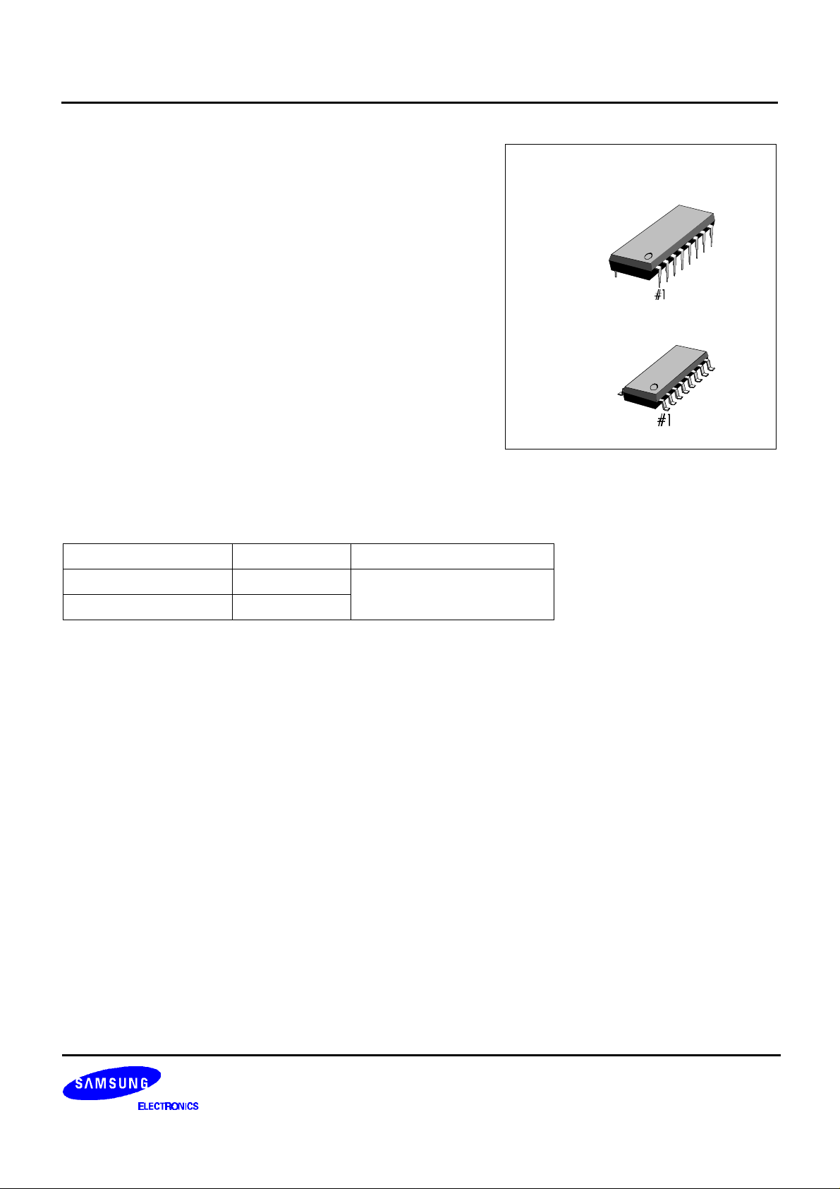
ORDERING INFORMATION
Device Package Operating Temperature
S5T8803A01-D0B0 16−DIP−300A
−30°C to +75°C
S5T8803A01-S0B0 16−SOP−225
16−DIP−300A
16−SOP−225
1

S5T8803A 10 CH PLL
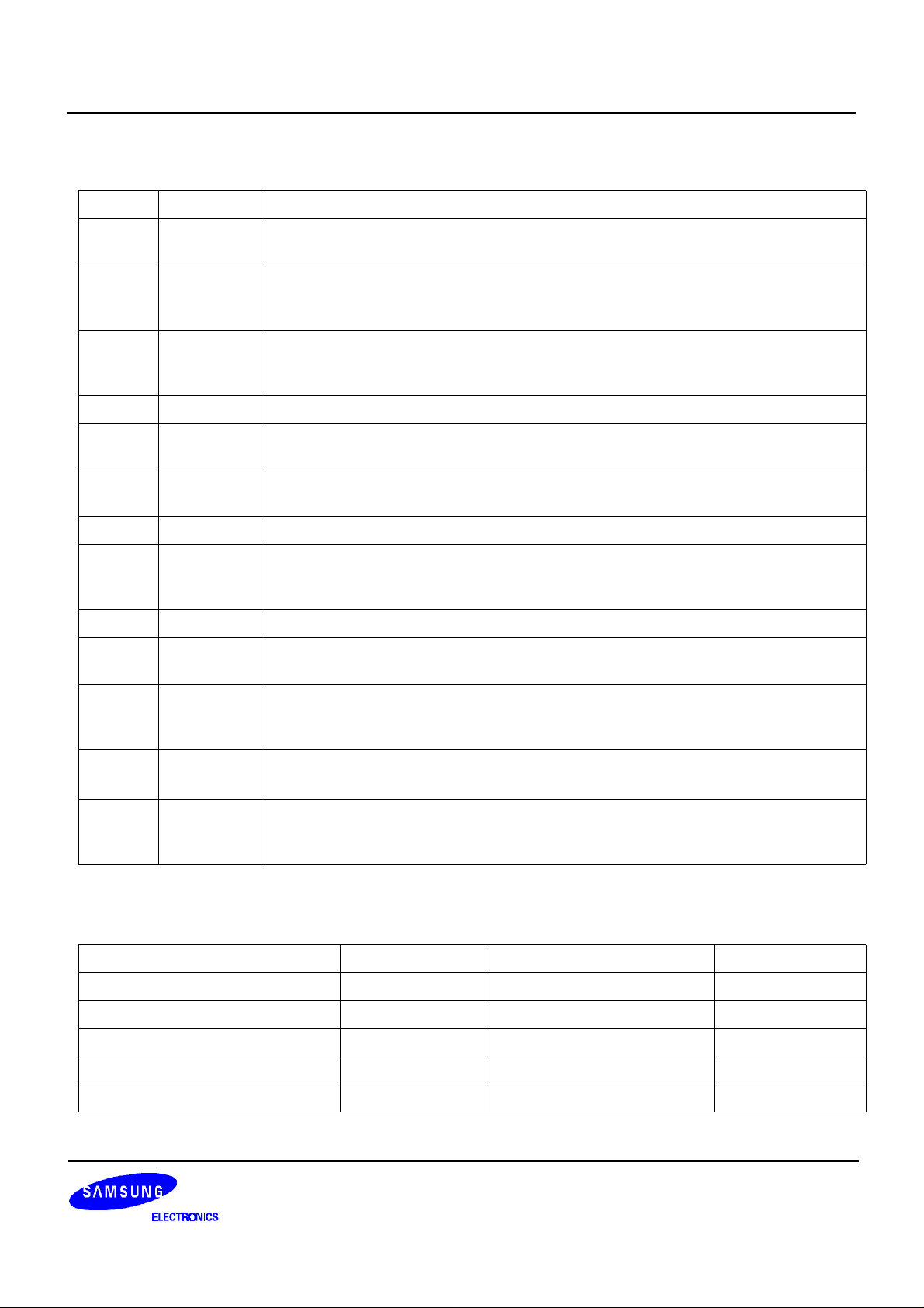
BLOCK DIAGRAM
OSCI
16
OSCO
1
PDT
11
TIF
9
PIN CONFIGURATION
V
DD
15
REFERENCE
DIVIDER
PHASE
DETECTOR (Tx)
PROGRAMMABLE
DIVIDER (Tx)
DECODER
PROGRAMMABLE
5 6 7 8
SB D0 D1 D2 D3 MODE
V
SS
12
PHASE
DETECTOR (Rx)
DIVIDER (Rx)
UNLOCK
DETECTOR
23
V
DD
+
F1
4
PDR
13
14
RIF
+
10
LDT
OSCO
MODE
SB
F1
D0
D1
D2
D3
1
2
3
4
5
6
7
8
S5T8803A
16
15
14
13
12
11
10
9
OSCI
V
DD
RIF
PDR
V
SS
PDT
LDT
TIF
2
10 CH PLL S5T8803A
PIN DESCRIPTION
Pin No Symbol Description
1 OSCO This output generates the reference frequency when it is connected to Pin 16 with the
external OSC, whose frequency is 10.24MHz.
2 MODE Base/Remote Unit Selection Pin.
“High”: Base Unit
“Low” : Remote Unit
3 SB Standby pin. This input controls Tx PLL for reducing the power dissipation
“High”: Normal operation
“Low”: Standby
4 F1 5KHz output
5, 6
7, 8
D0, D1
D2, D3
Channel selection pins
The Combinations of these inputs select one channel among the 10 channels
9 TIF Input to programmable divider of Tx. AC coupling with VCO
In case of a larger signal, It needs DC−coupling. Minimum input voltage is 0.1 Vrms
10 LDT Unlocked signal out pin (see output characteristics)
11 PDT Phase detector output for Tx.
PDT detects the phase error from Tx PLL and its output is connected to the external
low pass filter
12 VSS This pin is the negative supply of the IC. It is usually grounded
13 PDR Phase detector output for Rx. PDR detects the phase error from Rx PLL and its output
is connected to the external low pass filter
14 RIF Input of programmable divider for Rx. AC coupling with VCO
In case of a larger signal (standard CMOS logic), it needs DC coupling.
Minimum input voltage is 0.1Vrms
15 V
DD
This pin is the positive supply of the IC
Its reference is VSS, and normally + 3.0V ~ + 5.5V more positive than V
SS
16 OSCI X-TAL OSC connection pin
This input generates the reference frequency when it is connected to pin 1 with the
external OSC
ABSOLUTE MAXIMUM RATINGS
Characteristic Symbol Value Unit
Supply voltage V
Input Voltage V
Power Dissipation P
Operating Temperature T
Storage Temperature T
DD
I
D
OPR
STG
−0.5 ~ +6.0 V
−0.3 ~ VDD + 0.5 V
350 mW
−30 ~ + 75 °C
−40 ~ + 125 °C
3
 Loading...