Samsung S5T8555X01-L0B0 Datasheet

TIME SLOT ASSIGNMENT CIRCUIT S5T8555
INTRODUCTION
The S5T8555 is a per channel Time Slot Assignment Circuit (TSAC)
that produces 8-bit receive and transmit time slots for four 1 CHIP
CODEC.
Each frame synchronization pulse may be independently assigned
to a time slot in a frame of up to 64 time slots
FEATURES
• Single, 5V operation
• Low power consumption: 5mW
• Controls four 1 CHIP CODEC
• Independent transmit and receive frame syncs
• channel unidirectional mode
• Up to 64 time slots per frame
• Compatible with S5T8554B/7B CODECs
• TTL and CMOS compatible
20-CERDIP
ORDERING INFORMATION
Device Package Operating Temperature
S5T8555X01-L0B0 20−CERDIP −20°C to 125°C
1

S5T8555 TIME SLOT ASSIGNMENT CIRCUIT
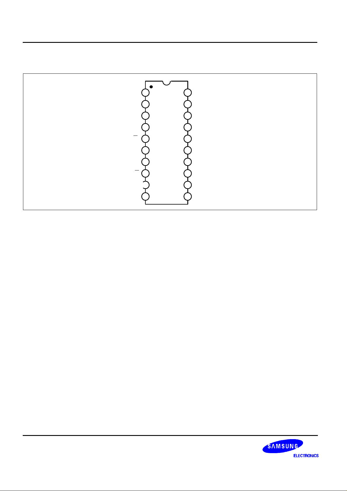
PIN CONFIGURATION
FSX1
FSR1
FSX0
FSR0
TS
X
1
2
3
4
5
KT8555
S5T8555
V
20
CC
FSR2
19
FSX2
18
FSR3
17
FSX3
16
CLK
CS
MODE
GND
D
6
C
7
C
8
9
15
14
13
12
1110
CH0
CH1
RSYC/CH2
XSY
C
BCLK
2

TIME SLOT ASSIGNMENT CIRCUIT S5T8555
PIN DISCRIPTION
Pin No Symbol Description
3
1
18
16
4
2
19
17
5 TS
6 D
7 CLK
FSX0
FSX1
FSX2
FSX3
FSR0
FSR1
FSR2
FSR3
X
C
A Transmit frame sync output which is normally low, and goes active-high for 8 cycles
of BCLK when a valid transmit time slot assignment is made.
A Receive frame sync output which is normally low, and goes active-high for 8 cycles
of BCLK when a valid receive time slot assignment is made.
This pin pulls low during any active transmit time slot. (N-channel open drain)
The input for an 8 bit serial control word. X is the first bit clocked in.
C
The clock input for the control interface.
8 CS The active-low chip select for the control interface.
9 MODE Mode 1 = Open or V
CC
Mode 2 = Gnd
10 GND Ground
11 BCLK The bit clock input (2.048 MHz)
12 XSY
C
The transmit Time Slot Output sync pulse input. Must be synchronous with BCLK.
13 RSYC /CH2 The receive time slot sync pulse input. Must be synchronous with BCLK. In mode 1
this input is the receive time slot 0 sync pulse, RSYC, which must be synchronous
with BCLK. In mode 2 this is the CH2 input for the MSB of the channel select word.
14 CH1 The input for the NSB (next significant bit) of the channel select word.
15 CH0 The input for the LSB (last significant bit) of the channel select word, which defines
the frame sync output affected by the following control word.
20 V
CC
Power supply pin. 5V ± 5%
3
 Loading...