

Samsung S5N8952X Datasheet

S5N8952X
ADSL Transceiver for NIC
Preliminary Information
(Revision 2.0)
September. 2000
SAMSUNG ELECTRONICS CONFIDENTIAL PROPRIETARY
Copyright ©1999-2000 Samsung Electronics, Inc. All Rights Reserved

S5N8952X
ADSL Transceiver for NIC
Preliminary Information (Rev.2.0)
Contents
1. Features.......................................................................................................... 5
2. General Description........................................................................................... 5
3. Logical Symbol Diagram .................................................................................... 6
4. Pin Configuration.............................................................................................. 7
5. Pin Description................................................................................................. 8
6. Functional Description..................................................................................... 13
7. I/O Timing Description..................................................................................... 14
8. Electrical Characteristics.................................................................................. 16
9. Package Description........................................................................................ 17
2

S5N8952X
ADSL Transceiver for NIC
Preliminary Information (Rev.2.0)
List of Figures
Figure 1: General Block Diagram.........................................................................5
Figure 2: Logical Symbol Diagram of the S5N8952X.............................................6
Figure 3: Pin Configuration of the S5N8952X ......................................................7
Figure 4: Functional Block Diagram of the S5N8952X......................................... 13
Figure 5: AFE Data I/F Timing Diagram.............................................................. 14
Figure 6: AFE Control I/F Timing Diagram.......................................................... 14
Figure 7: PCI I/F Timing Diagram......................................................................15
Figure 8: 208-LQFP Package Diagram............................................................... 17
3

S5N8952X
ADSL Transceiver for NIC
Preliminary Information (Rev.2.0)
List of Tables
Table 1: Pin Description of the S5N8952X ..........................................................8
Table 2: Absolute Maximum Ratings................................................................. 16
Table 3: Recommended Operating Conditions .................................................... 16
Table 4: Power Dissipation.............................................................................. 16
Table 5: DC Characteristics.............................................................................16
4

S5N8952X
ADSL Transceiver for NIC
Preliminary Information (Rev.2.0)
Processor
ATM
End
Hybrid
Line
Driver
DSP
PCI_BUS
S5N8952
S5N8951
1. Features
• Full Compliance with T1.413 Issue-2, ITU-T G.992.1 (G.dmt) and G.992.2 (G.lite).
• FDM and EC-based DMT Line Coding
• Data Rate: over 8Mbps for Downstream and 640 Kbps for Upstream.
• Reach: 6.7 Km (22Kft) with 24 AWG and 5.5 Km (18 Kft) with 26 AWG
• Supports Rate Adaptive Mode (steps of 32kbps)
• Reed-Solomon Forward Error Correction with(or without) Interleaver
• Adaptive Frequency and Time Domain Equalizer.
• Trellis Coding and Echo Cancellation.
• Supports Normal or Reduced Overhead Framing Modes
• Supports Analog and Digital PLL.
• Compatible to PCI V2.2
• Handle ATM Cells (On-Chip SAR and Connection Memory)
• Supports Fast Retraining Function in G.lite Mode
• Supports Network Management Function
• Supports Power Management Function
• 0.18µm, 1.8V CMOS Technology
• Operating Temperature: -40 °C to 85 °C
• Package Type: 208-LQFP
2. General Description
The S5N8952X is a complete ATM-based ADSL modem solution with associated F/W and
an Analog Front-End (S5N8951). The S5N8952X provides all the digital functions such as
PCI I/F, SAR, ATM framing, channel codec, DMT modulation, and DSP control.
There are two interfaces for external communications; PCI bus interface for NIC
applications and AD/DA interface. The S5N8952X is optimized for providing NIC solution
for CPE, and uses 17.664MHz Xtal oscillator as a master clock.
DMT
Framer
PCI
&
SAR
ROM
Analog
Front-
Phone
Figure 1: General Block Diagram
5
S5N8952X
ADSL Transceiver for NIC
Preliminary Information (Rev.2.0)
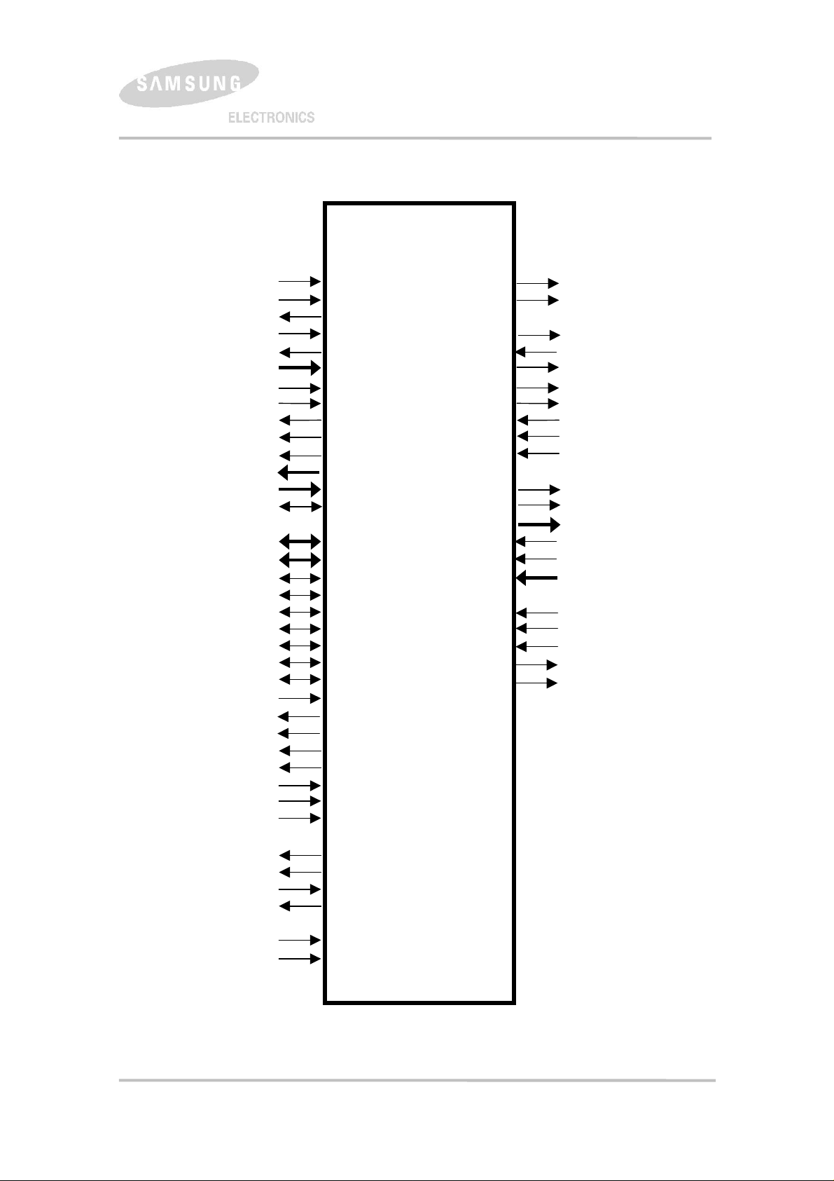
3. Logical Symbol Diagram
S5N8952X
RESET_N LD_TX_PWDN
XTAL_IN LD_RX_PWDN
XTAL_OUT
EXT_CLK AFE_RESET_N
PLL_FILT AFE_SDI
TEST_MODE[3:0] AFE_SDO
TEST_SCN_EN AFE_SCK
TEST_IN AFE_SEN_N
TEST_OUT AFE_BUSY
TX_SHOW AFE_PME
RX_SHOW AFE_NOISE
GP_OUT[1:0]
BT_MODE[1:0] AFE_DA_REF
NTR AFE_DA_CLK
PCI_AD[31:0] AFE_AD_REF
PCI_CBE_N[3:0] AFE_AD_CLK
PCI_FRAME_N AFE_AD_DAT[6:0]
PCI_IRDY_N
PCI_TRDY_N TL_TMS
PCI_DEVSEL_N TL_TCK
PCI_STOP_N TL_TDI
PCI_PERR_N TL_TDO
PCI_PAR TL_TINTP
PCI_GNT_N
PCI_PME_N
PCI_REQ_N
PCI_SERR_N
PCI_INTA_N
PCI_RST_N
PCI_CLK
PCI_IDSEL
AFE_DA_DAT[6:0]
EPROM_CS_N
EPROM_SI
EPROM_SO
EPROM_CK
PWR_ON
AUX_PWR_ON
Figure 2: Logical Symbol Diagram of the S5N8952X
6
 Loading...