

Samsung S5N8947X Datasheet

S5N8947X
MCU for ADSL/Cable Modem
(Revision 0.1)
May. 23, 2000
SAMSUNG ELECTRONICS PROPRIETARY
Copyright ©1999-2000 Samsung Electronics, Inc. All Rights Reserved

S5N8947 (ADSL/Cable Modem MCU)
ELECTRONICS
CONTENTS
1. GENERAL DESCRIPTION ................................................................................................................................ 4
2. FEATURES..........................................................................................................................................................5
3. FUNCTIONAL BLOCK DESCRIPTIONS.........................................................................................................6
3.1. BLOCK DIAGRAM.........................................................................................................................................6
3.2. ARCHITECTURE............................................................................................................................................7
3.3. SYSTEM MANAGER ...................................................................................................................................... 7
3.4. UNIFIED INSTRUCTION/DATA CACHE ............................................................................................................7
3.5. SAR/UTOPIA INTERFACE..............................................................................................................................7
3.6. ETHERNET MAC.......................................................................................................................................... 7
3.7. USB CONTROLLER ......................................................................................................................................8
3.8. DMA CONTROLLER.....................................................................................................................................8
3.9. UART (SERIAL I/O).....................................................................................................................................8
3.10. TIMERS....................................................................................................................................................8
3.11. PROGRAMMABLE I/O................................................................................................................................8
3.12. INTERRUPT CONTROLLER .........................................................................................................................8
3.13. I2C SERIAL INTERFACE.............................................................................................................................9
3.14. PLL (FOR SYSTEM/USB).......................................................................................................................... 9
4. PIN DESCRIPTIONS.........................................................................................................................................10
4.1. PIN CONFIGURATION.................................................................................................................................. 10
4.2. PIN DESCRIPTIONS .....................................................................................................................................11
4.3. PIN DESCRIPTIONS WITH THE PIN NUMBER AND PAD TYPE............................................................................13
5. OPERATION DESCRIPTION..........................................................................................................................16
5.1. CPU CORE OVERVIEW ...............................................................................................................................16
5.2. INSTRUCTION SET ......................................................................................................................................17
5.3. OPERATING STATES.............................................................................................................................17
5.4. OPERATING MODES .............................................................................................................................18
5.5. REGISTERS............................................................................................................................................. 18
5.6. EXCEPTIONS..........................................................................................................................................18
6. HARDWARE STRUCTURE.............................................................................................................................20
6.1. SYSTEM MANAGER ....................................................................................................................................20
6.1.3. Overview.........................................................................................................................................20
6.1.4. System Manager Registers...............................................................................................................20
6.1.5. System Memory Map.......................................................................................................................21
6.2. INSTRUCTION / DATA CACHE......................................................................................................................23
6.3. I2C BUS CONTROLLER................................................................................................................................24
6.4. ETHERNET CONTROLLER............................................................................................................................25
6.4.1. Block Diagram................................................................................................................................25
6.4.2. Features and Benefits ......................................................................................................................25
6.5. SAR AND UTOPIA INTERFACE.....................................................................................................................27
6.5.1. Block Diagram................................................................................................................................27
6.5.2. Features and Benefits ......................................................................................................................27
6.6. USB CONTROLLER ....................................................................................................................................28
6.6.1. Block Diagram................................................................................................................................28
6.7. DMA CONTROLLER...................................................................................................................................29
6.8. UART(SERIAL I/O)....................................................................................................................................30
6.9. TIMERS......................................................................................................................................................31
MagIC Team Page : 2 SAMSUNG ELECTRONICS

ELECTRONICS
S5N8947 (ADSL/Cable Modem MCU)
6.10. I/O PORTS..............................................................................................................................................32
6.11. INTERRUPT CONTROLLER........................................................................................................................33
7. SPECIAL FUNCTION REGISTERS ................................................................................................................34
8. ELECTRIC CHARACTERISTICS...................................................................................................................37
8.1. ABSOLUTE MAXIMUM RATINGS........................................................................................................37
8.2. RECOMMENDED OPERATING CONDITIONS ...................................................................................................37
8.3. DC ELECTRICAL CHARACTERISTICS ................................................................................................38
8.4. A.C ELECTRICAL CHARACTERISTICS........................................................................................................... 39
9. PACKAGE DIMENSION ..................................................................................................................................48
SAMSUNG ELECTRONICS Page : 3 MagIC Team

S5N8947 (ADSL/Cable Modem MCU)
ELECTRONICS
1. GENERAL DESCRIPTION
Samsung's S5N8947 16/32-bit RISC microcontroller is a cost-effective, high-performance
microcontroller solution. The S5N8947 is designed as an integrated Ethernet controller for use in managed
communication hubs and routers. The S5N8947 also provides ATM Layer SAR (Segmentation and
Reassembly) function with UTOPIA interface and the full-rate USB (Universal Serial Bus) function.
The S5N8947 is built around an outstanding CPU core: the 16/32-bit ARM7TDMI RISC processor
designed by Advanced RISC Machines, Ltd. The ARM7TDMI core is a low-power, general purpose,
microprocessor macro-cell that was developed for use in application-specific and custom-specific
integrated circuits. Its simple, elegant, and fully static design is particularly suitable for cost-sensitive and
power-sensitive applications.
Important peripheral functions including an UART channel, 2-channel GDMA, two 32-bit timers, I2C bus
controller, and programmable I/O ports are supported. Built-in logic including an interrupt controller,
DRAM controller, and a controller for ROM/SRAM and flash memory are also supported. The
S5N8947’s System Manager includes an internal 32-bit system bus arbiter and an external memory
controller.
To reduce total system cost, the S5N8947 offers a unified cache, Ethernet controller, SAR and USB. Most
of the on-chip function blocks have been designed using an HDL synthesizer and the S5N8947 has been
fully verified in Samsung's state-of-the-art ASIC test environment.
MagIC Team Page : 4 SAMSUNG ELECTRONICS

ELECTRONICS
S5N8947 (ADSL/Cable Modem MCU)
2. FEATURES
ü 4-Kbyte unified cache
ü SAR (Segmentation and Reassembly)
ü UTOPIA (the Universal Test & Operations PHY Interface for ATM) Level 2 Interface
ü Ethernet MAC
ü Full-rate USB controller
ü 2-CH GDMA (General Purpose Direct Memory Access)
ü UART (Universal Asynchronous Receiver and Transmtter)
ü 2 programmable 32bits Timers
ü 18 Programmable I/O ports
ü Interrupt controller
ü I2C controller
ü Built-in PLLs for System/USB
ü Cost effective JTAG-based debug solution
ü Boundary scan
ü Operating Voltage Range(2.5V +/- 0.2V)
ü Operating Frequency Up to 50MHz
ü 208 TQFP Package
SAMSUNG ELECTRONICS Page : 5 MagIC Team
S5N8947 (ADSL/Cable Modem MCU)
ELECTRONICS
3. FUNCTIONAL BLOCK DESCRIPTIONS
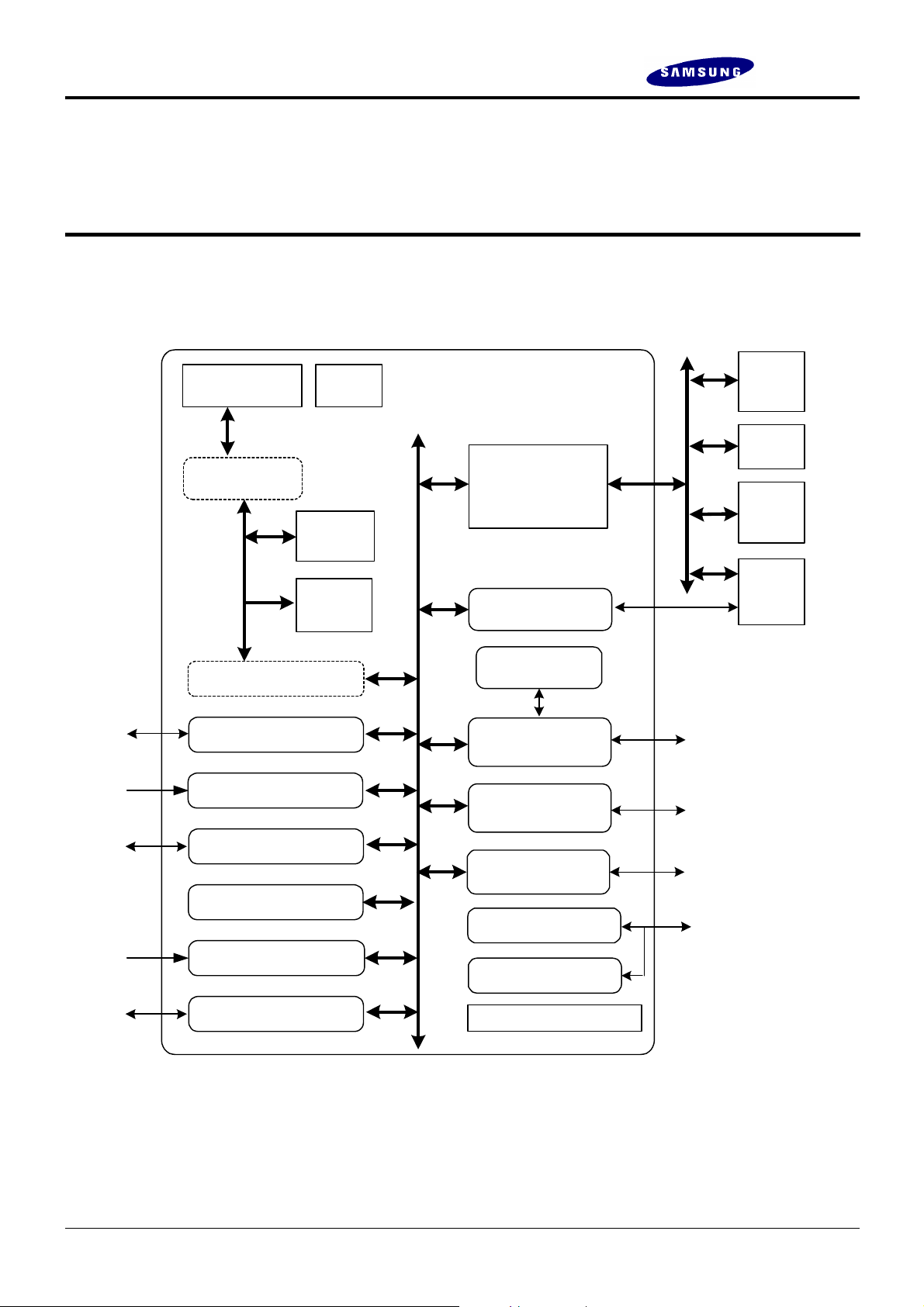
3.1. Block Diagram
ARM7TDMI
32bit RISC CPU
ICE
Breaker
4-Bank
ROM
SRAM
FLASH
CPU Interface
Bus Router
General I/O Ports
Interrupt Controller
UART
Unified
CACHE
4-word
Write
Buffer
32-bit
System
Bus
Memory
Controller
with
Refresh
Control
System Bus
Arbiter
Connection
Memory
SAR/UTOPIA
Ethernet MAC
USB Interface
4-Bank
DRAM
4-Bank
External
I/O
Device
External
Bus
Master
MagIC Team Page : 6 SAMSUNG ELECTRONICS
32bit Timer 0, 1
GDMA 0, 1
IIC Controller
PLL* (USB)
PLL* (System)
TAP Controller for JTAG
Figure 1 Top Block Diagram
X'tal Osc

ELECTRONICS
S5N8947 (ADSL/Cable Modem MCU)
3.2. Architecture
Integrated system for embedded Ethernet / USB / SAR
Fully 16/32-bit RISC architecture
Efficient and powerful ARM7TDMI core
Little/Big-Endian mode is supported basically, but the internal architecture is big-endian.
Cost-effective JTAG-based debug solution
Supports Boundary Scan
3.3. System Manager
8/16/32-bit external bus support for ROM/SRAM, flash memory, DRAM and external I/O
One external bus master with bus request/acknowledge pins
Supports for EDO/normal or SDRAM
Programmable access cycle
Four-word depth write buffer
Cost-effective memory-to-peripheral DMA interface
3.4. Unified Instruction/Data Cache
Two-way set-associative unified cache (4Kbytes)
Supports for LRU (least recently used) Protocol
Cache is configurable as internal SRAM
3.5. SAR/Utopia Interface
Directly supports ATM Adaptation Layer Five (AAL5) Segmentation And Reassembly
Segments and reassembles data up to 70Mbps
A glueless UTOPIA level 2 interface is supprted (for receiving and transmitting ATM cells with SAR, it
is a standard ATM interface between ATM link and physical layer).
3.6. Ethernet MAC
2 DMA engines with burst mode
Full compliance with IEEE standard 802.3
Supports MII interface (7-wire 10-Mbps interface is also supported).
SAMSUNG ELECTRONICS Page : 7 MagIC Team

S5N8947 (ADSL/Cable Modem MCU)
ELECTRONICS
3.7. USB Controller
Supports 12Mbps full rate function for universal serial bus
3.8. DMA Controller
2-channel general purpose DMA (for memory-to-memory, memory-to-USB, USB-to-memory, UARTto-memeory, memory-to-UART data transfers without CPU intervention)
Initiated by a software or a external DMA request
Increments or decrements source or destination address in 8-bit, 16-bit or 32-bit data transfers
3.9. UART (Serial I/O)
UART (Serial I/O) block with DMA-based or interrupt-based operation
Supports for 5-bit, 6-bit, 7-bit, or 8-bit serial data transmit and receive
Programmable baud rates
Infra-red (IR) TX/RX support (IrDA)
3.10. Timers
Two programmable 32-bit timers
Interval mode or toggle mode operation
Supports a watchdog timer.
3.11. Programmable I/O
18 programmable I/O ports
Pins individually configurable to input, output, or I/O mode for dedicated signals
3.12. Interrupt Controller
18 interrupt sources, including 4 external interrupt sources
Normal or fast interrupt mode (IRQ, FIQ)
Prioritized interrupt handling
MagIC Team Page : 8 SAMSUNG ELECTRONICS

ELECTRONICS
S5N8947 (ADSL/Cable Modem MCU)
3.13. I2C Serial Interface
Single Master mode operation only
3.14. PLL (for System/USB)
The external clock can be multiplied by on-chip PLLs to provide high frequency System/USB clock
The input frequency is fixed to 12 MHz
The output frequency is 4.167 times the input clock for System.
The output frequency is 4 times the input clock for USB.
SAMSUNG ELECTRONICS Page : 9 MagIC Team

S5N8947 (ADSL/Cable Modem MCU)
ELECTRONICS
4. PIN DESCRIPTIONS
4.1. Pin Configuration
156
155
154
153
152
151
150
149
148
147
146
145
144
143
142
VSS
VDD
157
VDD
VSS
158
159
UTO_RXADR[0]
160
UTO_RXADR[1]
UTO_RXADR[2]
161
162
UTO_RXD[0]
UTO_RXD[1]
163
164
UTO_RXD[2]
165
UTO_RXD[3]
UTO_RXD[4]
166
167
UTO_RXD[5]
UTO_RXD[6]
168
169
UTO_RXD[7]
170
UTO_RXSOC
UTO_RXENB
171
172
UTO_RXCLAV
UTO_CLK
173
174
VDD
175
VSS
SCL
176
177
SDA
UCLK
178
UARXD
179
180
UATXD
nUADTR
181
182
nUADSR
MDC
183
MDIO
184
185
COL
RXD[0]
186
187
RXD[1]
188
RXD[2]
RXD[3]
189
190
RX_DV
VDD
191
192
VSS
193
RX_CLK
RX_ERR
194
195
TX_CLK
TXD[0]
196
197
TXD[1]
198
TXD[2]
TXD[3]
199
200
TX_EN
TX_ERR
201
202
CRS
203
USB_DP
USB_DN
204
205
TMODE
CLKSEL
206
207
VDD
208
VSS
UTO_TXENB
UTO_TXSOC
UTO_TXD[7]
UTO_TXD[6]
UTO_TXCLAV
UTO_TXD[5]
UTO_TXD[4]
UTO_TXD[3]
UTO_TXD[2]
UTO_TXD[1]
UTO_TXD[0]
UTO_TXADR[2]
UTO_TXADR[1]
141
140
139
138
137
136
135
134
133
132
131
130
129
128
127
126
125
124
VSS
VDD
PP[17]
PP[16]
PP[15]
UTO_TXADR[0]
PP[14]
PP[13]
PP[12]
PP[11]
PP[9]
PP[10]
PP[8]
PP[7]
PP[6]
PP[5]
PP[4]
PP[3]
S5N8947
208-TQFP-2828
(Top View)
123
VSS
122
VDD
121
120
PP[2]
PP[1]
119
118
117
PP[0]
XDATA[31]
XDATA[30]
116
115
114
113
XDATA[29]
XDATA[28]
XDATA[27]
XDATA[26]
112
111
110
109
XDATA[25]
XDATA[24]
XDATA[23]
XDATA[22]
108
107
106
105
VSS
VDD
XDATA[21]
XDATA[20]
XDATA[19]
XDATA[18]
XDATA[17]
XDATA[16]
XDATA[15]
XDATA[14]
XDATA[13]
XDATA[12]
XDATA[11]
XDATA[10]
XDATA[9]
XDATA[8]
XDATA[7]
XDATA[6]
XDATA[5]
XDATA[4]
XDATA[3]
XDATA[2]
XDATA[1]
XDATA[0]
ADDR[21]
ADDR[20]
ADDR[19]
ADDR[18]
ADDR[17]
ADDR[16]
ADDR[15]
ADDR[14]
ADDR[13]
ADDR[12]
ADDR[11]
ADDR[10]
ADDR[9]
ADDR[8]
ADDR[7]
ADDR[6]
ADDR[5]
ADDR[4]
ADDR[3]
ADDR[2]
ADDR[1]
ADDR[0]
nWBE[3]
nWBE[2]
VSS
VDD
VSS
VDD
VSS
VDD
VSS
VDD
104
103
102
101
100
99
98
97
96
95
94
93
92
91
90
89
88
87
86
85
84
83
82
81
80
79
78
77
76
75
74
73
72
71
70
69
68
67
66
65
64
63
62
61
60
59
58
57
56
55
54
53
MagIC Team Page : 10 SAMSUNG ELECTRONICS
VDD
VSS
OSC_XIN
OSC_XO
XCLK_I
VSS
FILTER_S
VDDA_S
VSSA_S
FILTER_U
VDDA_U
VSSA_U
nTRST
TDI
TDO
TMS
TCK
CLKOEN
MCLKO
VDD
VSS
nRESET
B0SIZE[0]
B0SIZE[1]
ExtMREQ
ExtMACK
BIGEND
nDTACK
nOE
nECS[0]
nECS[1]
nECS[2]
nECS[3]
nRCS[0]
VDD
VSS
nRCS[1]
nRCS[2]
nRCS[3]
nRAS[0]
nRAS[1]
nRAS[2]
nRAS[3]
nCAS[0]
nCAS[1]
nCAS[2]
nCAS[3]
nDWE
nWBE[0]
123456789101112131415161718192021222324252627282930313233343536373839404142434445464748495051
nWBE[1]
Figure 2 S5N8947 Pin Configuration
VDD
VSS
52
ELECTRONICS
S5N8947 (ADSL/Cable Modem MCU)
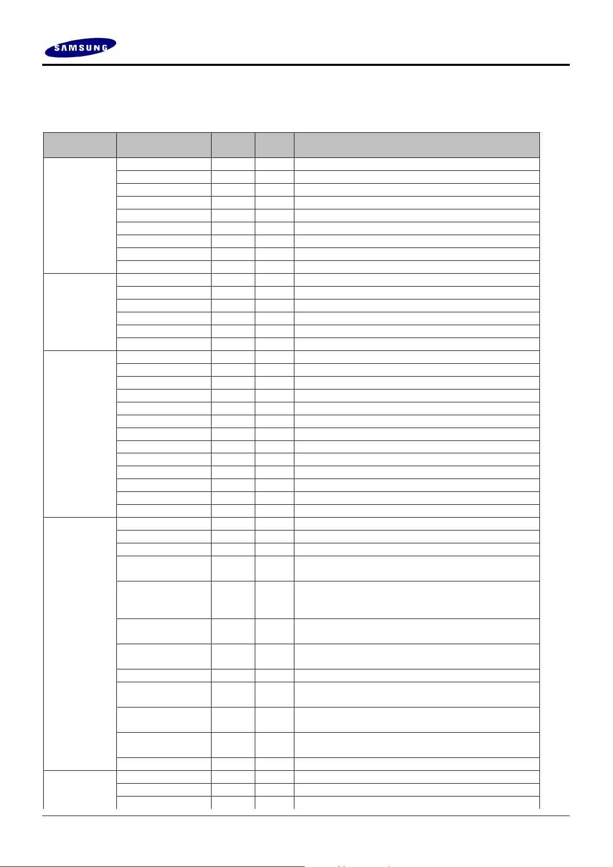
4.2. Pin Descriptions
Group Pin Name
XCLK_I 1 I External System Clock Source Input.
MCLKO 1 O System Clock Out.
CLKSEL 1 I Clock Frequency Select from the internal PLL.
System
Configurations
(9)
TAP
Control
(5)
Memory
Interface
(81)
Ethernet
Controller
(18)
UART
(5)
nRESET 1 I System Reset, Low Active.
CLKOEN 1 I System Clock Out Enable.
BIGEND 1 I Big endian mode select pin.
FILTER_S 1 O PLL filter pin for System Clock Generation.
OSC_XIN 1 I 12MHz Reference Clock.
OSC_XO 1 O Crystal Clock Output.
TMODE 1 I Test Mode Enable.
TCK 1 I JTAG Test Clock Input.
TMS 1 I JTAG Test Mode Select.
TDI 1 I JTAG Test Data Input.
TDO 1 O JTAG Test Data Output.
nTRST 1 I JTAG Reset Signal, Low Active.
ADDR[21:0] 22 O Address Bus.
XDATA[31:0] 32 I/O External Bidirectional 32bit Data Bus.
nRAS[3:0] 4 O Row AddressSstrobe for DRAM, Low Active.
nCAS[3:0] 4 O Column Address Strobe for DRAM, Low Active.
nDWE 1 O Write Enable, Low Active.
nECS[3:0] 4 I/O External I/O Select, Low Active.
nDTACK 1 I External Data Acknowledge Signal.
nRCS[3:0] 4 O ROM/SRAM/Flash Chip Select, Low Active.
B0SIZE[1:0] 2 I Bank 0 Data Bus Size for Boot ROM.
nOE 1 O Output Enable, Low Active.
nWBE[3:0] 4 O Write Byte Enable, Low Active.
ExtMREQ 1 I External Master Bus Request.
ExtMACK 1 O External Bus Acknowledge.
MCD 1 O Management data clock.
MDIO 1 I/O Management data I/O.
COL/COL_10M 1 I Collision detected/Collision detected for 10M.
TX_CLK/
TX_CLK_10M
TXD[3:0]/
TXD_10M/
LOOP_10M
TX_EN/
TXEN_10M
TX_ERR/
PCOMP_10M
CRS/CRS_10M 1 I Carrier sense/Carrier sense for 10M.
RX_CLK/
RXCLK_10M
RXD[3:0]/
RXD_10M
RX_DV/
LINK_10M
RX_ERR 1 I Receive error.
UCLK 1 I External Clock Input for UART.
UARXD 1 I UART Receive Data.
UATXD 1 O UART Transmit Data.
Pin
Counts
1 I Transmit clk/Transmit clk for 10M.
4 O Transmit data/Transmit data for 10M.
1 O Transmit enable/Transmit enable for 10M.
1 O Transmit error/Packet compression enable for 10M.
1 I Receive clock/Receive clock for 10M.
4 I Receive data/Receive data for 10M.
1 I Receive data valid.
I/O
Type
Description
SAMSUNG ELECTRONICS Page : 11 MagIC Team
S5N8947 (ADSL/Cable Modem MCU)
ELECTRONICS
nUADTR 1 I UART Data Terminal Ready, Low Active.
nUADSR 1 O UART Data Set Ready, Low Active.
P[7:0] 8 I/O General I/O ports for Bi-directional Data Only.
General
Purpose
In/Out
Ports
(including
xINTREQ
nXDREQ
nXDACK
TIMER0,1)
(18)
I2C
(2)
Utopia
(Level 2)
(30)
USB
(3)
xINTREQ[3:0]
/P[11:8]
XDREQ[1:0]/
P[13:12]
nXDACK[1:0]/
P[15:14]
TIMER0/
P[16]
TIMER1/
P[17]
4 I/O External Interrupt Requests/General I/O Ports.
2 I/O External DMA Requests for GDMA/General I/O Ports.
2 I/O
1 I/O TIMER0 Out/General I/O Port.
1 I/O TIMER1 Out /General I/O Port.
SCL 1 I/O I2C Serial Clock.
SDA 1 I/O I2C Seral Data.
UTO_TXADR[2:0] 3 O Transmit Address Bus.
UTO_TXD[7:0] 8 O Transmit Data Bus to the ATM PHY.
UTO_TXSOC 1 O Start Of Cell Indicator for Transmit Data.
UTO_TXENB 1 O Transmit Data Transfer Enable, Low Active.
UTO_TXCLAV 1 I Cell Buffer Available for Transmit Data.
UTO_TXADR[2:0] 3 O Receive Address Bus.
UTO_RXD[7:0] 8 I Receive Data Bus from the ATM PHY.
UTO_RXSOC 1 I Start Of Cell Indicator for Receive Data.
UTO_RXENB 1 O Receive Data Transfer Enable, Low Active.
UTO_RXCLAV 1 I Cell Buffer Available for Receive Data.
UTO_CLK 1 O Transfer/Receive interface byte clock.
USB_DP 1 I/O USB data D+
USB_DN 1 I/O USB data DFILTER_U 1 O USB PLL filter pin.
External DMA Acknowledge from GDMA/General I/O
Ports.
Table 1 Signal Pin Descriptions for Each Group
MagIC Team Page : 12 SAMSUNG ELECTRONICS

ELECTRONICS
S5N8947 (ADSL/Cable Modem MCU)
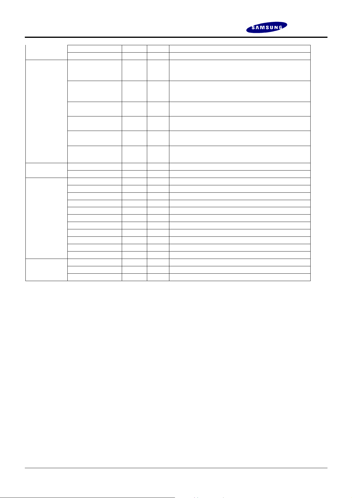
4.3. Pin Descriptions with the Pin number and Pad type
Pin
No
1 VDD
2 VSS
3 OSC_XIN I 12MHz reference clock
4 OSC_XO O
5 XCLK_I I ptic S5N8947 System Source Clock
6 VSS
7 FILTER_S O Poa_bb System PLL filter pin
8 VDDA_S PWR vdda Analog power for PLL
9 VSSA/VBBA_S GND vbba Analog / bulk ground for PLL
10 FILTER_U O poa_bb USB PLL filter pin
11 VDDA_U PWR vdda Analog power for PLL
12 VSSA/VBBA_U GND vssa Analog / bulk ground for PLL
13 nTRST I pticu JTAG Not Reset
14 TDI I pticu JTAG Test Data In
15 TDO O ptot2 JTAG Test Data Out
16 TMS I pticu JTAG Test Mode Select
17 TCK I ptic JTAG Test Clock
18 CLKOEN I ptic Clock Out Enable/Disable
19 MCLKO O pob8 System Clock Out
20 VDD PWR
21 VSS GND
22 nRESET I ptis Not Reset
23-24 B0SIZE[0:1] I ptic Bank 0 Data Bus Access Size
25 ExtMREQ I ptic External Master bus request
26 ExtMACK O pob1 External bus Acknowledge
27 BIGEND I pticd Big endian mode select pin
28 nDACK I ptic Not external acknowledge signal
29 nOE O ptot4 Not output enable
30-33 nECS[0:3] B pbct4 Not external I/O select
34-39 nRCS[0:3] O ptot4 Not ROM/SRAM/Flash Chip select
40-43 nRAS[0:3] O ptot4 Not Row address strobe for DRAM
44-47 nCAS[0:3] O ptot4 Not Column address strobe for DRAM
48 nDWE O ptot4 Not Write Enable
49-50 NWBE[0:1] O ptot4 Not Write Byte Enable
51 VDD PWR
52 VSS GND
53 VDD PWR
54 VSS GND
55-56 NWBE[2:3] O ptot4 Not Write Byte Enable
57-69 ADDR[0:12] O ptot6 Address bus
70 VDD PWR
71 VSS GND
72-80 ADDR[13:21] O ptot6 Address bus
81-86 XDATA[0:5] B ptbsut6 External bidirectional data bus
87 VDD PWR
88 VSS GND
89102
103 VDD PWR
104 VSS GND
Pin Name
XDATA[6:19] B ptbsut6 External bidirectional data bus
I/O
Type
Pad type Descriptions
Psoscm2
USB crystal clock out
SAMSUNG ELECTRONICS Page : 13 MagIC Team

S5N8947 (ADSL/Cable Modem MCU)
ELECTRONICS
107-
118
119-
121
XDATA[20:31] B ptbsut6 External bidirectional data bus
P[0:2] B ptbst4sm General I/O ports
122 VDD_P PWR
123 VSS_P GND
124-
138
P[3:17] B ptbst4sm General I/O ports
139 VDD_P PWR
140 VDD_S GND
141-
143
144-
151
UTO_TXADR[0:2] O Address bus for TX
UTO_TXD[0:7] O pob4 Data bus for TX
152 UTO_TXSOC O pob4 Start Of Cell for TX
153 UTO_TXENB O pob4 Enable data transfers (active low)
154 UTO_TXCLAV I ptis Cell Buffer Available
155 VDD_P PWR vdd3op I/O pad power
156 VSS_P GND vssop I/O pad ground
157 VDD_P PWR vdd3op I/O pad power
158 VSS_P GND vssop I/O pad ground
159-
161
162-
169
UTOP_RXADR[0:2] O Address bus for RX
UTO_RXD[0:7] I ptis Data bus for RX
170 UTO_RXSOC I ptic Start Of Cell for RX
171 UTO_RXENB O pob4 Enable data transfers (active low)
172 UTO_RXCLAV I ptis Cell Buffer available
173 UTO_CLK O pob4 Transfer/Receive interface byte clock
174 VDD_I PWR
175 VSS_I GND
176 SCL B ptbcd4 I2C serial clock
177 SDA B ptbcd4 I2C serial data
178 UCLK I ptis UART external clock for UART
179 UARXD I ptic UART receive data
180 UATXD O pob4 UART transmit data
181 nUADTR I ptic Not UART0 data terminal ready
182 nUADSR O pob4 Not UART0 data set ready
183 MDC O pob4 Management data clock
184 MDIO O ptbbcut4 Management data I/O
185 COL/COL_10M I ptis Collision detected/Collision detected for 10M
186-
189
RXD[0:3]/RXD_10M I ptis Receive data/Receive data for 10M
190 RX_DV/LINK_10M I ptis Receive data valid
191 VDD PWR
192 VSS GND
193
RX_CLK/RXCLK_10
M
I ptis Receive clock/Receive clock for 10M
194 RX_ERR I ptis Receive error
195
196-
199
TX_CLK/TX_CLK_10
M
TXD[0:3]/TXD_10M/
LOOP_10M
I ptis Transmit clock/Transmit clock for 10M
O pob4 Transmit data/Transmit data for 10M
200 TX_EN/TXEN_10M O pob4 Transmit enable/Transmit enable for 10M
201
TX_ERR/PCOMP_10
M
O pob4 Transmit error/Packet compression enable for 10M
202 CRS/CRS_10M I ptis Carrier sense/Carrier sense for 10M
MagIC Team Page : 14 SAMSUNG ELECTRONICS

ELECTRONICS
S5N8947 (ADSL/Cable Modem MCU)
203 USB_DP B USB data D+
204 USB_DN B
pbusb1
USB data D205 TMODE I ptic Test Mode
206 CLKSEL I ptic Clock Out Enable/Disable
207 VDD PWR
208 VSS GND
SAMSUNG ELECTRONICS Page : 15 MagIC Team
 Loading...